Note: Descriptions are shown in the official language in which they were submitted.
1 '
2178292
1 - 94-PDC-476
LOW COST APPARATUS FOR DETECTING ARCING
FAULTS AND CIRCUIT BREAKER INCORPORATING SAME
BACKGROUND OF THE INVENTION
Field of the Invention
This invention relates to apparatus responsive to arcing faults and circuit
breakers incorporating same, and more particularly such apparatus preferably
utilizing
analog circuits.
Background Information
Conventional circuit breakers respond to overcurrents and short circuits
to interrupt current in a protected circuit. Some circuit breakers also
protect personnel
and equipment from ground currents. Recently, there has been increased
interest in
providing protection against arcing faults. Arcing faults can occur for
instance between
adjacent bared conductors, between exposed ends of broken conductors, at a
faulty
connection and in other situations where conducting elements are in close
proximity.
Arcing faults in ac systems can be intermittent as the magnetic repulsion
forces generated by the arc current force the conductors apart to extinguish
the arc.
Mechanical forces then bring the conductors together again so that another arc
is
struck.
Arcing faults typically have high resistance so that the arcing current is
below the instantaneous or magnetic trip thresholds of protection in a typical
circuit
breaker. Also, the intermittent nature of an arcing fault can create an
average RMS
current value which is below the thermal threshold for the circuit breaker
Even so, the
arcs can cause injury or start a fire if they occur near combustible material.
It is not
practical to simply lower the pick-up currents on conventional circuit
breakers as there
2178292
- 2 - 94-PDC-476
are many typical loads which draw similar currents, and would therefore, cause
nuisance trips.
Much attention has been directed toward trying to distinguish arcing
currents from other intermittent currents. It has been recognized that arcing
currents
generate a step increase in current when the arc is struck. However, many
typical
loads generate a similar step increase when a device is tumed on. In many
instances,
the step increases generated by these loads are singular events while an
arcing fault
generates a series of step increases. One fault detector counts the step
increases and
generates a trip signal if a selected number of step increases occur within a
given
interval. However, there are loads such as a solid state dimmer switch which
also
generates step increases in current when the firing angle is phased back
substantially.
It has also been recognized that arcing faults generate a great deal of
high frequency noise, and further, that there are periods of quiescence in the
high
frequency component. Some circuit breakers look to such features to
differentiate
arcing faults from other phenomena. Circuit breakers which rely upon such
detailed
characteristics of current waveforms to detect arcing faults typically utilize
a
microprocessor to perform the analysis. They also require fairly good quality
analog-
to-digital converters to capture the high frequencies of interest. Thus, such
arcing fault
detectors add significantly to the cost of a circuit breaker, and in the case
of a typical
residential circuit breaker, can multiply its cost many times. Yet even such
sophisticated arc detecting circuit breakers are subject to nuisance trips
when
confronted with some common load devices.
There is a need therefore, for an improved circuit breaker for providing
protection against arcing faults which is economically practical. In this
regard, there
is a need for such a circuit breaker which can reliably respond to arcing
faults and
which does not require a microprocessor and associated high quality analog to
digital
converters.
SUMMARY OF THE INVENTIOAI
These needs and others are satisfied by the invention which is directed
to apparatus for detecting an arcing fault and circuit breakers incorporating
such
apparatus both having a simple, low cost circuit to detect arcing faults.
Rather than
analyzing the high frequency noise which accompanies an arcing current, this
circuit
responds to a step increase in current accompanying each striking of the arc,
and the
~ 2178292
- 3 - 94-PDC-476
repetitive occurrence of the arc. More particularly, it responds to the
accumulated,
time attenuated amplitude of the step increases in current. The greater the
amplitude
of the step increase in current caused by striking of the arc the fewer step
increases are
needed to detect the arcing current. In fact, if the arcing current is
sufficiently high,
a single strildng of the arc will be sufficient to indicate the presence of
the arc. In
order to reduce nuisance tripping, a preferred embodiment of the invention
only
responds to step increases in current which exceed those associated with
common
loads, such as for instance dimmer switches and irons with a bi-metal
thermostat.
In particular, an analog circuit in accordance with the invention includes
sensing means which, in the preferred embodiment, is the bi-metal of the
thermal trip
unit commonly found in small circuit breakers. The voltage across the sensing
means,
which represents load current, is converted to pulses having an amplitude
proportional
to the amplitude of the step increase in load current by one or more low pass
filters
combined with one or more high pass filters. These pulses are full wave
rectified and
converted to current pulses by a circuit which responds to the very low
amplitude pulse
signals output by the filter. These current pulses are then applied to a
capacitor which
integrates them with respect to time. The charge on the capacitor is
continuously
adjusted so that the voltage across the capacitor represents the accumulated,
time
attenuated amplitude of the pulses. A current slightly greater than the
magnitude of
pulses which would be generated by common loads is subtracted from the current
pulses before they are applied to the capacitor to reduce the chances of a
nuisance trip.
Also, a current can be subtracted from the capacitor to further reduce the
possibility
of nuisance tripping. A non-linear transfer function can be applied to the
current
pulses before or after the bias current is subtracted to provide better
response to arcing
faults while avoiding nuisance trips. Preferably, the non-linear function is a
convex
function, i.e., a function in which the slope is never negative. In a specific
embodiment of the invention, the non-linear function is a squaring function.
As
another aspect of the invention, the arcing fault detector is preferably used
together
with a ground fault interrupter which we have found responds to high
resistance line-to-
ground faults such as can be caused by failures in wiring devices such as
receptacles.
Carbonization produced by the arcing provides a path to ground which results
in
tripping of the ground fault circuit at arcing currents below the threshold of
the arcing
fault detector which is necessarily set high enough to avoid nuisance trips.
CA 02178292 2004-10-05
- 4 - 94-PDC-476
BRIEF DESCRIPTION OF THE DRAWINGS
A full understanding of the invention can be gained from the following
description of the preferred embodiments when read in conjunction with the
accompanying drawings in which:
Figure 1 is a schematic diagram of a circuit breaker in accordance with
the invention.
Figure 2A illustrates a waveform associated with a typical arcing current
to which the circuit breaker of Figure 1 responds.
Figure 2B is a waveform diagram illustrating a pulse signal generated
by the circuit breaker of Figure 1 in response to the arcing current shown in
Figure
2A.
Figure 2C is a waveform diagram showing the pulses of Figure 2B after
they have been further processed by the circuit breaker of Figure 1.
Figure 2D is a waveform diagram illustrating the voltage produced on
a capacitor forming part of the circuit of Figure 1 by the pulses of Figure
2C.
Figure 3A and 3B together illustrate a schematic circuit diagram of
another embodiment of a circuit breaker in accordance with the invention.
Figure 4 is a plot illustrating the response of the circuit breaker shown
in Figures 3A and 3B.
DESCRIPTION OF THE PREFERRED EMBODIMENT
The invention will be described as applied to a miniature circuit breaker
such as that described in U.S. patent number 4,081,852.
That circuit breaker incorporates a thermal-magnetic trip device
comprising a bi-metal and a magnetic armature which unlatch a spring driven
mechanism to open the contacts in response to a persistent overcurrent and a
short
circuit current, respectively. The circuit breaker of patent number 4,081, 852
includes
a ground fault detector which can be replaced by, or be used in addition to,
the arcing
fault detector which forms a part of the present invention.
Turning to Figure 1, the electrical system 1 protected by the circuit
breaker 3 includes a line conductor 5 and a neutral conductor 7 connected to
provide
power to a load 9. The circuit breaker 3 includes separable contacts 11 which
can be
tripped open by a spring operated trip mechanism 13. The trip mechanism 13 may
be
actuated by a conventional thermal-magnetic overcurrent device 15. This
thermal-
2178292
- 5 - 94-PDC-476
magnetic overcurrent device 15 includes a bi-meta( 17 connected in series with
the line
conductor 5. Persistent overcurrents heat up the bi-rnetal 17 causing it to
bend and
release a latch 19 which actuates the trip mechanism 13. Short circuit
currents through
the bi-metal 17 magnetically attract an armature 21 which alternatively
releases the
latch 19 to actuate the trip mechanism 13.
In addition to the thermal-magnetic overcurrent device 15 which provides
conventional protection, the circuit breaker 3 provides an arcing fault
detector 23. This
arcing fault detector 23 includes a pair of leads 25 and 27 connected to sense
voltage
across the bi-metal 17. As the resistance of the bi-metal 17 is known (for the
exemplary bi-metal, about 0.0025 ohms), this voltage is a measure of the
current
flowing through the line conductor 5.
The arcing fault detector 23 is a trip circuit which responds to an inverse
relationship between the magnitude of step increases in current produced by
the striking
of an arc in the electrical system 1, and the rate at which such arcs are
struck. This
arcing fault detector 23 includes a pulse generating circuit 29 which
generates a pulse
having a magnitude proportional to the magnitude of the step increase in
current
produced by the striking of the arc. This pulse generating circuit includes a
filter 31
which in turn includes a first high pass filter 33 made up of a series
capacitor 35 and
shunt resistor 37, a low pass filter 39 made up of the series resistor 41 and
shunt
capacitor 43 and a second high pass filter 45 made up of the series capacitor
47 and
shunt resistor 49. The electrical system 1 commonly has a resistive plus
inductive
impedance which is variable. The time constants of the low pass filter 39 and
the
combined high pass filters 33 and 45 are selected to be below the electrical
system
response so that the amplitude of the filter output will be constant,
regardless of the
electrical system rise time. Further, the filter response must be chosen to
provide
sufficient attention at the power line frequency, e.g., 60 Hz. The response of
the hlter
31 to step increases in currents produced by an arcing fault is a pulse having
a
magnitude proportional to the magnitude of the step increase produced by
striking of
the arcing current. These pulses will have the polarity of the half cycle in
which the
arc is struck. For an arcing current which strikes each half cycle and is
extinguished
at zero crossings, the pulses will alternate in polarity.
The pulse generating circuit 29 also includes a rectifier circuit 51 for
converting the bi-polar pulses output by the filter 31 into a single polarity
pulse signal.
~ 2178292
- 6 - 94-PDC-476
A conventional diode bridge c2nnot be used to rectify the pulses because the
diode
voltage drops in the conventional rectifier exceed the millivolt signals
produced by an
arcing fault across the bi-metal 17. In addition, the rectifier circuit 51
converts the
voltage pulses produced by the filter 31 into current pulses required by the
trip signal
generating circuit which follows.
The rectifier circuit 51 includes a differential amplifier 53 formed by the
transistors 55 and 57. These transistors are connected through resistors 59
and 61 to
a constant current source 63 formed by the transistor 65 supplied with a
constant base
bias provided by the diode 67 and a resistor 69 energized by the supply
voltage bus 71.
A current mirror 73 formed by the transistors 75 and 77 is connected between
the
supply voltage bus 71 and the collectors of the transistors 55 and 57. As is
well
known, the current mirror 73 operates to maintain the current imi equal to the
current
it . With no output from the filter 31, the constant current provided by the
constant
current source 65 is evenly divided between ii and i,. Since the current tm,
is equal
to the current ii it is also equal to the current i. Whenever the filter 31
generates a
positive pulse in response to the striking of an arcing current during a
positive half
cycle of current on the line conductor 5, the transistor 55 is turned on more
than the
transistor 57 so that more of the constant current provided by the constant
current
source 65 flows through that transistor. Hence, the current ii exceeds the
current i, .
Since the current mirror 73 causes the current imi to equal the current 1t ,
i., exceeds i,
and a current i flows out of the node 79 between the current mirror 73 and the
transistor 57 on the lead 81.
The lead 81 is connected to the emitter of an npn transistor 83 and the
emitter of the pnp transistor 85. The bases of the transistors 83 and 85 are
biased by
one-half the supply voltage by the ladder of zener diodes 87. With the current
i
tlowing out of the node 79, the transistor 85 is turned on to direct the
current i to the
lead 89.
When the arcing current strikes on a negative half cycle of current on
a line conductor 5, a negative pulse is output by the filter 31. Such negative
pulses
turn on the transistor 57 harder than the transistor 55 so that the current i,
exceeds the
current i, . Therefore, the current iml is smaller than the current i, and the
currenti
2178292
- 7 - 94-PDC-476
is reversed and flows into the node 79. This tums off the transistor 85 and
turns on
the transistor 83. The negative current i flowing through the transistor 83 is
mirrored
by the mirror circuit 91 formed by the transistors 93 and 95 to produce the
currenti
on the lead 89. Thus, despite the polarity of pulses generated by the filter
31, pulses
of a single polarity appear on the lead 89.
As mentioned, there are some loads which generate repetitive step
increases in current which could be mistaken for arcing faults. Therefore, the
present
invention only responds to step increases in current which exceed those
generated by
common loads. This is accomplished by subtracting from the single polarity
pulses
appearing on the lead 89 a reference current iR produced by a constant current
source
97 formed by the transistor 99 having constant bias applied to its base by a
diode 101
and resistor 103 connected to the supply voltage bus 71. The portion by which
the
current pulses f exceed the threshold represented by the reference current iR
flows to
ground through transistor 104 and charges a capacitor 105 through a current
mirror 107
formed by the transistors 109 and 111. When the amplitude of the pulses i do
not
exceed the reference voltage 1R no current flows through the mirror 106, and
hence the
charge on the capacitor is not affected.
The voltage across the capacitor 105 is compared in a comparator 115
to a reference voltage set at about one-half the voltage on the supply bus 71
by the
zener diodes 87. The capacitor 105 integrates with respect to time the amount
by
which the current pulses exceed the reference current iR while the resistor
113 adjusts
the charge accumulated by continuously bleeding charge from the capacitor. The
values of the capacitor 105 and the resistor 113 are selected to provide the
desired
accumulated, time attenuated pulse amplitude function. While the pulses
produced by
the striking of the arcing current can occur randomly, especially where the
magnetic
forces separate the conductors to extinguish the arc, the arc is struck
repetitively
thereby producing a series of pulses over time. Hence more pulses are required
to
reach the threshold voltage on the capacitor when the amplitude of the arcing
current
is low than would be required for larger arcing currents. In fact, a single
pulse of
sufficient amplitude will generate an output on the comparator 115. The output
of the
comparator 115 applies through the resistors 117 and 119 a turn-on voltage to
the gate
of an SCR 121. Tum-on of the SCR 121 energizes a trip coil 123 which releases
the
~ 2178292
- 8 - 94-PDC-476
latch 19 on the trip mechanism 113 to open the contacts 11. The SCR is
protected
from voltage surges by the varistor 125 and its gate is protected from noise
by a
capacitor 127. Current for the detector circuit 23 is drawn from the neutral
conductor
7 through the coil 1 and 23, and is halfwave rectified by the diode 129 and
filtered by
the filter 131 to produce the dc supply voltage on the supply voltage bus 71.
The
capacitor 105, resistor 113 and comparator 115 form a trip signal generator
116 which
turns on the SCR 121.
Figures 2A, 2B, 2C and 2D illustrate waveforms that are present at
particular points in the circuit in Figure 1. Figure 2A illustrates a typical
arcing
current waveform 133. As can be seen, when the arc is struck a step increase
in
current is generated at 135. The arcing current is extinguished as it
approaches 0. It
remains 0 until the voltage on the negative half cycle reaches sufficient
amplitude to
strike the arc and a negative step increase in current 137 is generated. If
the
conductors are forced apart by the magnetic forces produced by the current,
the arc
would not be struck on the subsequent half cycle and it may be several cycles
before
the conductors again come close enough for the arcing current to strike again.
This
can occur randomly so that the polarity of the step increases in current can
be random.
It will be noticed that there is some high frequency noise 139 on the arcing
waveform.
It is this high frequency component which many arcing fault detectors look
for. The
detector circuit of the present invention only responds to the step increases
in current.
Figure 2B illustrates the pulse waveform which is output by the filter 31.
As indicated, these pulses 141 can be of either polarity. Figure 2C
illustrates the
single polarity pulses 143 which appear on the lead 89 at the output of the
rectifier
circuit 51. Figure 2C also illustrates that only the portions of the pulses
143 that
exceed the reference current fR are applied to the integrating capacitor 105.
Figure 2D
illustrates the voltage V, on the capacitor 105. As can be seen, each pulse
adds charge
to the capacitor which increases its voltage. Between pulses, the voltage
decays as the
charge is bled by resistor 113. If the pulses are of large enough amplitude
and occur
frequently enough, the voltage on the capacitor 105 reaches the trip voltage
V,
represented by the reference voltage applied to comparator 115, and the SCR
121 is
fired to trip the circuit breaker.
~ 2178292
9- 94-PDC-476
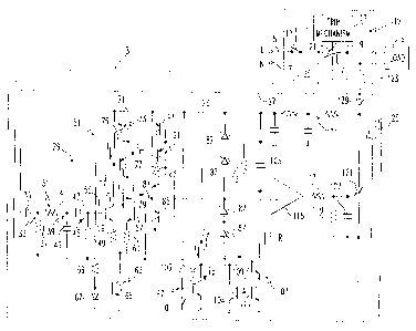
Figures 3A and 3B illustrate another embodiment of the invention
wherein like components are identified by like reference characters and
wherein
components similar to those in the circuit of Figure 1 are identified by the
same
reference character primed. The major difference between the circuit of
Figures 3A
and 3B and the circuit of Figure 1 is that the second embodiment of the
invention
squares the current pulses before the reference current is subtracted. The
arcing fault
detector 231 of Figures 3a and 3b like that of Figure 1 utilizes the voltage
generated
across the bimetal 17 as a measure of current flowing in the line conductor.
The pulse
generating circuit 29' includes the filter 31 comprising a high-pass filter
33, a low-pass
filter 39, and a second high-pass filter 45, having time constants selected as
discussed
in connection with Figure 1 so that the response of the filter 31 to step
increases in
currents produced by an arcing fault is a pulse having a magnitude
proportional to the
magnitude of the step increase produced by striking of the arcing current.
Again, these
pulses have the polarity of the half cycle in which the arc is struck.
The pulse generating circuit 291 also includes the rectifier circuit 51, for
converting the bi-polar pulses output by the filter 31 into a single polarity
pulse signal.
The rectifier circuit 511 includes the differential amplifier 531 formed by
the transistors
55 and 57, the emitters of which are connected by a resistor 145. These
emitters are
also connected to a constant current source 147 formed by the transistors 149
and 151,
having a common base drive provided by a transistor 153 energized through
resistor
155.
The rectifier circuit 511 also includes the current mirror 731 comprising
the transistors 157, 159, and 161. As discussed in connection with Figure 1,
the
current mirror 731 assures that the current im, remains equal to the current
if. When
the onset of an arc causes the filter circuit 31 to apply a positive pulse to
the
differential amplifier 531, the transistor 55 is turned on harder than the
transistor 57.
This results in current flowing through the resistor 145 which reduces the
current i2.
Thus, a current i flows out of the node 79. This current pulse, being
positive, tums
on the transistor 85 to produce a pulse on the lead 89.
When the filter 31 applies a negative pulse to the differential amplifier
53', the polarity of the current i at node 79 reverses and a transistor 83 is
turned on.
~ 2178292
- 10 - 94-PDC-476
The current mirror 911 formed by the transistors 163, 165, and 167 produces a
pulse
of positive polarity on the lead 89.
A circuit 169 applies a selected transfer function to the unipolar pulses
generated on the lead 89. Preferably, the transfer function is a convex
function, that
is, the slope of the function is never negative. In the exemplary embodiment
of the
invention, the circuit 169 is a squaring circuit which squares the pulses on
the lead 89.
This circuit 169 includes a pair of transistors 171 and 173 connected
between the lead 89 and ground. The lead 89 is also connected to the base of a
transistor 175 which has its emitter connected to the base of a grounded
emitter
transistor 177. The pulses on the lead 89 pass through the transistors 171 and
173
producing voltage drops Vt and VZ , respectively. The sum of the emitter-to-
base
voltages V3 and V4 of the transistors 177 and 175 equals the sum of the
voltages Vl
and V2. A constant current source formed by a transistor 179 having its base
drive
fixed by the transistor 181 which is connected to the power supply bus 71
through the
resistor 183 draws a constant current through the transistor 175. As the
transistor 175
has a high gain, and therefore draws negligible current through its base, the
voltage V4
is fixed by the bias current ib drawn by the constant current source. As is
known, the
voltages V1 to V4 are a function of the log of the current through the
respective
transistors. Thus, the following relationship applies:
log i1+log t2_1og i3+log t4
and, therefore:
l1Xi2-j3x=b
since il and i2 are both equal to ij,, (the current pulses on lead 89):
2
iyi = !3 x:B
.2
tL,
and, 13 = - = io~
Lb
The squared pulses are amplified by a current mirror 185 having an
input transistor 187 and a pair of output transistors 189 and 191 so that a
gain of two
is applied to the squared pulses.
2178292
- 11 - 94-PDC-476
In order to preclude nuisance trips caused by common loads, a reference
current t, is subtracted from the amplified squared pulse signal by a constant
current
source 97' which comprises a transistor 193 having constant base drive current
provided by the transistor 195 energized through the resistor 197. The
resultant pulses
which exceed the threshold current iR are provided on the lead 199.
Turning to Figure 3B, these clipped pulses on the lead 199 are applied
to the trip signal generator 116'. The trip signal generator 116' includes an
integrating
capacitor 105. The capacitor 105 is charged from the power supply lead 71
through
a resistor 113'. When the circuit is first turned on, a rapid charging circuit
203
initially brings the capacitor 105 up to full charge. This rapid charging
circuit 203
includes a pair of transistors 205 and 207 connected in parallel between the
power
supply lead 71 and the capacitor 105. Base drive to turn on these transistors
is
provided through a capacitor 211. The resistor 209, by diverting some of the
charging
current. establishes a minimum level of dv/dt required to turn on the
transistors 207
and 209. When the capacitor 211 becomes fully charged, the transistors 207 and
209
are turned off, and subsequent charging of the capacitor 105 is through the
resistor
113'.
The capacitor 105 of the trip signal generating circuit 116' integrates the
clipped pulses provided on the lead 199. Each pulse turns on a transistor 213
to turn
on a transistor 215 which, in turn, turns on a transistor 217 which drains
charge from
the capacitor 105 in proportion to the magnitude and duration of the pulse.
Successive
pulses reduce the voltage on the capacitor 105; however, the resistor 113'
continuously
applies charging current to the capacitor 105. The parameters are selected
such that
the selected function of the accumulated, time attenuated amount by which the
magnitude of the squared pulses exceeds the reference current is implemented.
When
the voltage on the capacitor 105 reaches the reference voltage on the
comparator 115'
formed by the transistors 219 and 221, which is the supply voltage (+13 volts)
minus
the diode drops of these two transistors, the transistors 219 and 221 are
turned on.
This turns on a pair of transistors 223 and 225 which latch the transistor 215
full-on
to generate a positive trip signal on the lead 227 through transistor 229.
This trip
signal turns on the SCR 121 to energize the trip coil 123.
CA 02178292 2004-10-05
- 12 - 94-PDC-476
Preferably, the sputtering arc fault detector 231 is used together with a
ground current detection circuit such as the ground fault circuit 231 or an
earth leakage
protection circuit (not shown), which are used for people protection and
equipment
protection, respectively. Preferably, the ground fault interrupting circuit
231 is of the
dormant oscillator type such as is shown in U.S. patent number 5,224,006.
Such a dormant oscillator type ground fault
interrupting circuit includes two pick-up coils. The first coil 233 is a
toroidal coil
through which both the line and neutral conductors 5 and 7 pass. Only the
neutral
conductor 7 passes through the second toroidal coil 235.
The ground current detection circuit such as ground fault circuit 231 is
particularly useful in combination with the arcing fault detector. As
mentioned, the
arcing fault detector 231 is subject to nuisance trips caused by some common
loads
which produce waveforms similar to those caused by arcing faults. Thus, the
magnitude of the step increases in current to which the arcing fault detector
responds
must be set high enough to avoid response to common loads which can produce a
similar step increase. We have found that arcing conditions such as can be
created in
wiring devices such as receptacles by faulty connections cause carbonization
which can
lead to tripping of the ground fault interrupter at arcing currents which are
below the
response level of the arcing fault detector. Thus, the ground fault
interrupter 231
extends protection against arcing faults. The trip signal generated by the
ground fault
interrupting circuit 231 turns on the SCR 121 through the lead 237 to energize
the trip
solenoid 123.
The ground fault detector 231 and the arcing fault detector 231 can be
implemented on a single integrated circuit chip (not shown). Certain of the
components of the arcing fault detector 231 could be implemented by discrete
components off of the chip to provide for easy modification of the circuit for
different
applications. For instance, the input filter 31 could be provided by discrete
components in order to adjust the sensitivity of the arcing fault detector. In
addition,
the capacitor 105 and charging resistor 201 could be discrete elements
selected to
provide the desired inverse relationship between the amplitude of the pulses
and the
arcing rate. In connection with this, the resistor 209 and capacitor 211 which
form
part of the circuit 203 for initially charging the capacitor 105 could also be
selectable
~ 2178292
- 13 - 94-PDC-476
off chip components. It may also be desirable to make the resistor of the
threshold
circuit 971 a discrete resistor to adjust the threshold level.
Figure 4 illustrates the inverse relationship between the amplitude of the
pulses generated by the onset of the arcing current and the number of pulses
required
to generate a trip signal. As can be seen from Figure 4 the amplitude of the
pulses
must exceed the threshold value represented by iR in order to generate a trip
signal.
On the other hand a single step increase in current of about 90 amps in the
example
will trip the circuit breaker.
Four traces A-D representing several ratios of half cycles in which an
arc is struck to the total number of half cycles are shown in Figure 4. For
instance,
trace A illustrates the response curve wherein an arc is initiated during each
half cycle
and thus is extinguished at each zero crossing. The trace B represents the
instance
wherein an arc is initiated once every three half cycles, while trace C
illustrates a duty
cycle of an arc struck every seven half cycles and trace D represents the
response for
a duty cycle in which an arc is struck only every 15 half cycles.
As can be appreciated, the invention provides a simple, low cost detector
for distinguishing arcing faults from normally encountered loads which also
distort the
current waveform in electrical distribution systems. This simple circuit
provides
variable response dependent upon the amplitude of the step increases in
current
produced by the striking of the arcing current and the time intervals at which
repetitive
pulses occur.
While specific embodiments of the invention have been described in
detail, it will be appreciated by those skilled in the art that various
modifications and
alternatives to those details could be developed in light of the overall
teachings of the
disclosure. Accordingly, the particular arrangements disclosed are meant to be
illustrative only and not limiting as to the scope of invention which is to be
given the
full breadth of the claims appended and any and all equivalents thereof.