Note: Descriptions are shown in the official language in which they were submitted.
RD-24,211 217 8 3 8 9
_1_
SOLID STATE ARRAY WITH
SUPPLEMENTARY CROSSOVER
STRUCTURE
This invention relates generally to large area solid state
imager devices and specifically to address line crossover structures
for large area imager devices.
Solid state imaging devices can be used for detection of
incident radiation. Such imager devices typically comprise an array of
pixels with an associated matrix of rows and columns of address lines
to electrically access each pixel. Each pixel has a photosensor and a '
switching transistor, such as a thin film transistor (TFT), the gate of
which is coupled to a scan line and the source of which (or
alternatively, the drain) is coupled to a data line. These address lines
are used read the signal from respective pixel photosensors.
The various components in an imager device are formed
in layers on a substrate such that components are sandwiched within
the completed structure. For example, scan lines and data lines are
disposed in a matrix structure such that data lines overlie scan lines at
crossover points in each pixel of the array. Defects in the array, such
as short circuits between scan lines and data lines commonly appear
in crossover regions. Such defects can seriously degrade imager
performance, particularly in high performance imagers such as are
used in medical diagnostic imaging.
Typically, the TFT gate dielectric material is disposed
over the array so as to be disposed between the scan lines and
address lines at crossover points. Such single layer dielectrics are
subject to degradation that can result in a conductive path between
the scan and data lines in the crossover region, shorting the address
lines and degrading array performance. Typically, additional
dielectric material disposed on the array is disposed over the entire
RD-24,211
2178389
-2-
region of the scan lines and TFT channel regions of the array (having
been formed, for example, by the oxidation of the scan line and gate
electrode conductive material); this arrangement leads to degraded
TFT performance because of reduced capacitance in the TFT channel
region (and thus results in higher noise in the imager array).
Summaryr of the Invention
In accordance with this invention, a solid state array
structure, such as an imager or display device, is provided that has a
robust dielectric structure between address lines at crossover regions
in the array while maintaining thin film transistor (TFT) performance,
and further providing reduced data line capacitance and thus reduced
noise in the array.
A solid state array device in accordance with this
invention includes a plurality of pixels with associated respective TFT
switching transistors; a plurality of first address lines disposed in a first
layer of the array device; a plurality of second conductive address
lines disposed in a second layer of the array device, respective ones
of said first and second address lines being disposed substantially
perpendicular to one another in a matrix arrangement such that
respective ones of the second address lines overlie respective ones
of the first address lines at respective crossover regions; a TFT gate
dielectric layer disposed in a channel region of each of the pixel TFTs
and further being disposed over the first address lines; and a
crossover region supplemental dielectric layer disposed in respective
ones of the crossover regions between the first and second address
lines, but disposed so as to not extend over the TFT channel regions.
RD-24,211
2178389
-3-
Brief Description of the Drawings
The features of the invention believed to be novel are
set forth with particularity in the appended claims. The invention itself,
however, both as to organization and method of operation, together
with further objects and advantages thereof, may best be understood
by reference to the following description in conjunction with the
accompanying drawings in which like characters represent like parts
throughout the drawings, and in which:
Figure 1 (A) is a plan view of apportion of an array having
a crossover region in accordance with the present invention.
Figure 1 (B) is a cross-sectional view of the crossover
region taken along the lines I - I of Figure 1 (A).
Figure 2(A) is a plan view of a portion of an array in
accordance with another embodiment of the present invention.
Figure 2(B) is a cross-sectional view of the crossover
region taken along the lines I - I of Figure 2(A).
Detailed Description of the Invention
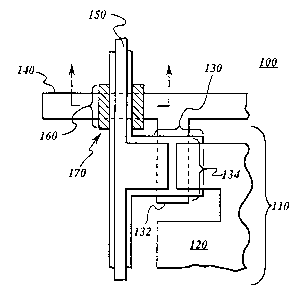
A solid state array device 100, such as a radiation
imager for detecting electromagnetic radiation such as x-rays or the
like, or a display device comprising liquid crystal devices, comprises a
plurality of pixels 110 (a representative portion of one pixel being
illustrated in Figure 1 (A)) and a plurality of first address lines 140 and
a plurality of second address lines 150 that are coupled to respective
ones of pixels 110, as illustrated in Figure 1 (A). By way of example,
and not limitation, the invention will be described with respect to a
RD-24,211
2178389
-4-
radiation imager using the nomenclature associated with such a
device; the invention is similarly applicable to an array structure used
in display devices. In a typical imager, each pixel 110 comprises a
respective photosensor 120 and a switching transistor 130, such as a
thin film transistor (TFT) or the like. In imager 100, first address lines
140 typically are referred to as scan lines and are coupled to a gate
132 of TFT 130; signals on these lines are used to cause the TFT to
become conductive or non-conductive. Second address lines 150
are typically referred to as data lines, and are coupled to respective
drains 134 of TFTs 130; the source of TFT 130 is coupled to
photosensor 120 (as used herein for TFT 130, both the source and
drain of the transistor are used for electrical coupling and the specific
nomenclature of source and drain is interchangeable). Scan lines
140 and data lines 150 are disposed in the array substantially
perpendicular to one another in a matrix arrangement such that data
lines 150 overlie scan lines at each pixel in a crossover region 160.
In accordance with this invention, imager 100 further
comprises a crossover region supplemental dielectric layer 170 that is
disposed between scan line 140 and data line 150 in crossover
region 160. As illustrated in Figure 1 (B), a cross-sectional view of
crossover region 160, scan line 140 is disposed on substrate 105 that
comprises glass or the like. Scan line 140 typically comprises a
conductive material such as aluminum, titanium, molybdenum, or the
like, and has a thickness in the range between about 0.1 pm and 1
p.m.
Typically supplemental dielectric layer 170 is disposed
directly on scan line 140, with a gate dielectric layer 136 disposed
over dielectric layer 170; alternatively, gate dielectric layer 136 is
disposed directly on scan line 140 and supplemental dielectric layer
170 is disposed over the gate dielectric layer (dependent on array
structure and fabrication techniques, dielectric layer 170 may be
disposed directly on scan line 140 or, alternatively, portions of the
semiconductor (e.g.., silicon) or conductor material (e.g., doped
RD-24,211
2178389
-5-
silicon) of the TFT sandwich structure can be disposed between the
scan line and dielectric layer 170). Gate dielectric layer 136 extends
over crossover region 160 and a channel region 134 of TFT 130 (the
channel region includes the area over gate electrode 132), and
typically is disposed across the array so as to electrically insulate
scan lines 140 from other array components. Gate dielectric layer
typically has a thickness in the range between about 0.1 ~,m and 0.5
~m and comprises an inorganic dielectric material such as silicon
oxide, silicon nitride, or silicon oxy-nitride, but may alternatively
comprise polyimide or similar polymer. In crossover region 160, data
line 150 is disposed over gate dielectric layer 136; in some
arrangements, such as illustrated in Figure 1 (A), data line 150 is
disposed on a semiconductive layer 138 that is typically formed from
the amorphous silicon deposited in the formation of TFT 130.
Semiconductive layer 138 typically has a thickness in the range
between about 0.05 p,m and 0.5 p.m. Additional layers (not pertinent
to the present invention ) of conductive, semiconductive, and
dielectric material (e.g., n+ type doped silicon deposited over the
silicon) are deposited in the formation of the imager array, but are not
shown for ease of illustration.
Supplemental dielectric layer 170 is disposed over scan
line 140 in crossover region 160 and comprises an electrically
insulative material such as an inorganic dielectric, for example silicon
oxide, silicon nitride, or the like, or alternatively, an organic dielectric,
for example a polymer material such as polyimide, or combinations
thereof. Inorganic dielectric material such as silicon oxide and silicon
nitride are readily deposited in a plasma enhanced chemical vapor
deposition (PECVD) process that is compatible with current array
fabrication techniques (e.g., for TFTs, address lines, and
photosensors). Organic dielectric materials such as polyimide are
also readily spun on and cured at this stage of the fabrication process
as the curing temperatures of about 300 'C do not have an adverse
effect on the array at the stage of the array fabrication process when
the supplemental dielectric layer is formed. The thickness of
RD-24,211
2178389
-s-
supplemental dielectric layer 170 is in the range between about 0.1
p.m and 1 pm for the inorganic dielectric materials, and up to several
microns thickness for organic dielectric materials.
The lateral extent (or boundaries) of supplemental
dielectric layer 170 typically extend beyond the immediate crossover
area (that is, the area of overlap of scan line 140 and data line 150)
so that the supplemental dielectric layer forms an island structure
centered on crossover region 160 and that extends up to about 3 p.m
(on either side, or a total of 6 p.m total difference in width) beyond the
lateral extent of scan line 140 or data line 150, as illustrated in Figure
1 (A) (in Figure 1 (A) and 2(A) the portion of supplemental dielectric
layer underlying data line 150 is shown in phantom). The
supplemental dielectric layer 170 island structure does not extend
into a channel region 134 of TFT 130; this structure provides
enhanced operation of the TFT and the array because the dielectric
thickness in the channel region is not greater than the thickness of the
gate dielectric layer. Additional dielectric thickness beyond that of the
gate dielectric layer has the effect of requiring an increase in the TFT
size to achieve acceptable transient response of the pixel.
Disadvantages of larger size TFTs include an increase of noise in the
array and higher required driving voltages than smaller size TFTs,
both of which degrade array performance.
In an alternative embodiment, crossover region
supplemental dielectric layer 170 comprises first tier 172 and a
second tier 174, as illustrated in Figure 2(B). In this arrangement,
second tier 174 comprises organic or inorganic dielectric material as
discussed above to provide the robust additional insulative protection
at the crossover region between scan lines 140 and data lines 150.
First tier 172 comprises a material that serves as an etch stop layer for
the dielectric material comprising second tier 174. The etch stop layer
minimizes any etching of glass substrate 105 during the etching steps
to pattern second tier 174 of the supplemental dielectric layer. As
used herein, "etch stop layer" or the like refers to a material that has
RD-24,211
2178389
_,_
an etch rate less than 20% of that of the overlying dielectric material in
second tier 174 (e.g., using the etchants commonly or typically used
in the art for etching of the dielectric material of second tier 174). For
example, inorganic dielectric materials silicon oxide and silicon
nitride comprising second tier 174 are commonly etched with a
solution of 10% buffered HF; etch stop layer 172 advantageously
comprises a semiconductive material such as amorphous silicon,
which etches at a slower rate (nominally zero) than the silicon nitride
or silicon oxide, which have an etch rate about 100 /min in the same
etchant. First tier etch stop layer 172 alternatively comprises a
conductive material which is etchable with an etchant that is specific
to the etch stop layer but not to the underlying scan line material.
Thus, etching of the etch stop layer would not result in etching of the
scan line material. For example, in embodiments in which scan lines
140 comprise titanium, molybdenum, or aluminum, chromium is
effectively used as first tier etch stop layer 172. The thickness of first
tier etch stop layer 172 is typically in the range between about 10 nm
and about 200 nm; the overall thickness of crossover region
supplemental dielectric layer is in the range between 0.1 ~m and
about 1 pm. In another alternative embodiment, the conductive
material comprising TFT gates and scan lines 140 is not patterned
prior to deposition of the supplemental dielectric layer so as to serve
as the etch stop when patterning the supplemental dielectric; in this
embodiment (not shown), the gate or scan line material underlies the
supplemental dielectric layer.
In a further alternative embodiment, crossover region
supplemental dielectric layer 170 is disposed in crossover region 160
and further disposed under the length of data line 150, as illustrated
in Figure 2(A). As noted above, supplemental dielectric layer 170
does not extend into channel region 134 of TFT 130. One advantage
of this embodiment is that when the supplemental dielectric layer is
disposed along the length of the data line, the data line conductive
material has fewer steps (changes in elevation as the line passes
over underlying components) along its length and thus in array
RD-24,211
~ 178389
_8_
fabrication fewer defects (or breaks) in the line occur, and hence the
structure results in a higher yield.
The present invention thus provides a robust dielectric
structure disposed between first address lines 140 (scan lines) and
second address lines 150 (data lines) in crossover regions 160 that
reduces the likelihood of electrical shorts between the crossing
address lines. The structure further is patterned such that it does not
degrade TFT characteristics as it does not extend into the channel
region of the TFT. The structure of the present invention thus provides
advantages over larger area dielectric structures, such as might be
obtained by oxidizing the upper portion of the first address line
conductive material to provide the additional dielectric structure (in
addition to the gate dielectric layer), because such a wide-area
oxidation process necessarily results in oxidation of the portion of the
first address line material that comprises the gate electrode of the
TFT. The structure of the present invention further reduces data line
capacitance, which is a major contributor to noise in a large area
(e.g., about 100 cm2 or larger) imager. Such capacitance reduction
results in the increased separation between the data line and the
scan line at crossover regions 160 (e.g., the increased separation
corresponding to the thickness of supplemental dielectric layer 170).
For example, in an imager having a pixel area of about 40,000 p,m2,
crossover supplemental dielectric layers 170 having a thickness of
about 1 p,m provide an array with a capacitance reduction between
scan and data lines of about 20 % over the equivalent array structure
without the supplemental dielectric layers.
It will be apparent to those skilled in the art that, while
the invention has been illustrated and described herein in
accordance with the patent statutes, modifications and changes may
be made in the disclosed embodiments without departing from the
true spirit and scope of the invention. It is, therefore, to be understood
that the appended claims are intended to cover all such modifications
and changes as fall within the true spirit of the invention.