Note: Descriptions are shown in the official language in which they were submitted.
2 i 79~77
RADIO TRANSMITTER/RECEIVER
BACKGROUND OF THE INV~N'1'ION
1. Field of the Invention
The present invention relates to a radio transmit-
ter/receiver which performs transmitting and receivingoperations simultaneously, more particularly to a radio
transmitter/receiver which comprises receiving local
oscillation means for producing a local oscillation
signal, which constitutes a phase lock loop-( PLL ) in-
cluding a dividing circuit to divide the local oscilla-
tion signal.
2. Description of the Related Art
Fig. 1 is a block diagram showing a constitution
example of a conventional radio transmitter/receiver.
It is noted that as such kind of a radio
transmitter/receiver there is, for example, a portable
telephone.
Here, a received signal Sl received through an
antenna 1 and a transmitting/receiving filter 2 is
mixed with a local oscillation signal S3 in a frequency
mixing circuit 3, and is converted into an intermediate
frequency signal. Thereafter, the intermediate fre-
quency signal is amplified in an intermediate frequency
circuit 4, and is output as the intermediate frequency
signal S2. It is noted that the local oscillation
21 7~777
-- 2
signal S3 is produced by a receiving local oscillation
means 8.
On the other hand, a transmitting signal S4 which
is output from a transmitting section 6 during talking
is transmitted through the transmitting/receiving
filter 2 and the antenna 1. In a standby period, re-
ceiving only is performed. In talking period, receiv-
ing and transmitting operations are performed simulta-
neously.
The receiving local oscillation means 8 comprises
a phase lock loop which is composed of a voltage con-
trol oscillation circuit ( VCO ) 81 outputting the
local oscillation signal S3, a dividing circuit 82
dividing the local oscillation signal S3, a reference
frequency oscillation circuit 83 producing a reference
signal, a phase comparison circuit 84 detecting the
phase difference between a dividing output and the
reference signal, a low pass filter 85 reducing a high
frequency component, and a rejection filter 86.
Hereupon, when a high level transmitting signal
interferes into a circuit of a receiving side during
talking, a reduction in a receiving sensitivity and an
incorrect operation of the receiving local oscillation
means are caused so that receiving function trouble is
caused. To reduce the occurrence of such troubles the
receiving side is shielded by the use of a metal plate
74570-46
21 7~777
having a shielding effect. To prevent the incorrect
operation of the receiving local oscillation means 8,
particularly, the rejection filter 86 are connected with
an input side of the dividing circuit 82.
Specifically, when the transmitting signal interferes
into the receiving local oscillation means 8 by spatial
propagation, and it is input to the dividing circuit 82
with a small level difference from the local oscilla-
tion signal S3, the dividing circuit 82 will perform an
incorrect operation so that a normal local oscillation
signal S3 is not produced. Particularly, in the equip-
ment which fits an antenna directly to its body, the
high level transmitting signal interferes thereinto. For
this reason, the receiving local oscillation means 8 is
designed such that by connecting the rejection filter
86 to the input side of the dividing circuit 82 the
interferingtransmitting signal is fully attenuated com-
pared with the local oscillation signal S3.
The rejection filter 86 is constituted such that
the filter 86 possesses the characteristic of being
able to attenuate the transmitting signal due to low
impedance for the frequency of the transmitting signal.
Furthermore, because the frequency of the local oscil-
lation signal S3 is close to that of the transmitting
signal S4, the local oscillation signal S3 to be passed
through is attenuated.
74570-46
2 1 7~777
The foregoing conventional radio
transmitter/receiver has a constitution such that the
dividing circuit connects the rejection filter to its
input side to attenuate the interferes transmitting
signal, in order to keep the dividing circuit from
performing incorrect operation by the transmitting
signal which interferes into the receiving local oscilla-
tion means formed of the PLL including the dividing
circuit.
This rejection filter, however, undesirably atten-
uates the local oscillation signal to be inherently
passed through, whereby the level of the local oscilla-
tion signal which is input to the dividing circuit is
reduced. Thus, the operation of the receiving local
oscillation means is stable. To compensate the passing
loss, when the level of the local oscillation signal is
increased, the receiving local oscillation means nor-
mally operates also in standby period. Consumed power
of the equipment increases. Particularly, for the
portable telephone which operates with a small capaci-
tançe cell, an operation time is short.
SUMMARY OF THE INV~;N'1'ION
The present invention was made considering the
foregoing problems involved in the foregoing conven-
tional prior arts, and the object of the present inven-
74570-46
2 1 7~777
.
- 5 -
tion is to provide a radio transmitter/receiver which
suppresses the power consumed to prevent incorrect
operation caused when a transmitting signal interferes
into a receiving local oscillation means constituted of
a PLL which a dividing circuit.
The foregoing object is accomplished in one embod-
iment by providing a radio transmitter/receiver com-
prising transmitting means for outputting a transmit-
ting -signal during talking; frequency mixing means for
normally receiving a receiving signal and a local
oscillation signal to mix these signals and to-output
an intermediate frequency signal; receiving local
oscillation means for constituting a phase locked loop
( PLL ) which includes a dividing circuit to divide the
aforementioned local oscillation signal and for produc-
ing the aforementioned local oscillation signal; trans-
mission detection means for detecting the aforemen-
tioned transmitting signal produced from an output side
of the aforementioned transmitting means to transmit a
detection signal; amplifying means which is disposed in
the input side of the aforementioned dividing circuit,
for amplifying the aforementioned local oscillation
signal by increasing the gain thereof upon the receipt
of the aforementioned detection signal; and filter
means which is disposed in the input side of the afore-
mentioned dividing circuit, for attenuating the fre-
74570-46
2 ~ 7~777
quency component of the aforementioned transmitting
signal interfering into the aforementioned dividing cir-
cuit upon the receipt of the aforementioned detection
signal.
In the foregoing constitution, the aforementioned
amplifying means includes an amplifying circuit which
changes the gain in accordance with a power source
current and a current source circuit which increases
the aforementioned power source current to be supplied
to the aforementioned amplifying circuit upon the
receipt of the aforementioned detection signal. The
aforementioned filter means includes a rejection filter
which exhibits a low impedance for the frequency of the
aforementioned transmitting signal and a switch which
is arranged between the rejection filter and the ground
and operates upon the receipt of the aforementioned
detection signal to make the aforementioned rejection
filter function.
The above and other objects, features, and advan-
tages of the present invention will become apparent
from the following ~escription referring to the accom-
panying drawings which illustrate an example of a
preferred embodiment of the present invention.
BRIEF DESCRIPTION OF THE DRAWINGS
Fig. 1 is a block diagram showing an example of a
74570-46
21 7~777
-- 7
conventional radio transmitter/receiver;
Fig. 2 is a block diagram showing an embodiment of
a radio transmitter/receiver according to the present
invention; and
Fig. 3 is a diagram showing the characteristic of
the rejection filter shown in Fig. 2.
DETAILED DESCRIPTION OF THE PREFERRED EMBODIMENTS
An embodiment cf a radio transmitting/receiver
according to the present invention will now be de-
scribed with reference to the accompanying drawings
below.
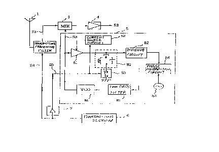
Fig. 2 is a block diagram showing an embodiment of
a radio transmitter/receiver according to the present
invention. Reference is now made to the drawing,
wherein like reference numerals designates correspond-
ing parts throughout the view.
Referring now to Fig. 2, a receiving signal Sl
received through an antenna 1 and a transmitting/re-
ceiving filter 2 is mixed with a local oscillation
signal S3 in a frequency mixing circuit 3 and is con-
verted to an intermediate frequency signal. Thereaf-
ter, the intermediate frequency signal is amplified in
an intermediate frequency amplifying circuit 4 and is
output as an intermediate frequency signal S2. It is
noted that the local oscillation signal S3 is produced
2 1 7~777
-- 8
by receiving local oscillation means 5.
On the other hand, a transmitting signal S4 which
is output from a transmitting section 6 during talking
is transmitted through the transmitting/receiving
filter 2 and the antenna 1. Furthermore, to detect the
transmitting signal S4 a transmitting detection circuit
7 is connected with an output side of the transmitting
section 6. When the transmitting signal S4 is output
from the transmitting section 6, the transmitting
detection circuit 7 detects the transmitting signal S4
and a transmitting detection signal S5 is output from
the transmitting detection circuit 7.
Next, receiving local oscillation means 5 will be
described.
Receiving local oscillation means 5 comprises a
voltage control oscillation circuit ( VCO ) 81 which
outputs the local oscillation signal S3, a dividing
circuit 82 which divides the local oscillation signal
S3, a reference frequency oscillation circuit 83 which
produces a reference signal, a phase comparison circuit
84 which detects the phase difference between a divided
output and the reference signal, a lowpass filter 85
which removes a high frequency component, and a rejec-
tion filter 86. These parts are the same as those of
the conventional radio transmitter/receiver. The
receiving local oscillation means 5 further comprises
74570-46
2 1 7~777
an amplifying circuit 51 which amplifies the local
oscillation signal S3 to transmit the signal S3 to the
dividing circ`uit 82, a current source circuit 52 which
controls the power source current to be supplied to the
amplifying circuit S1 in accordance with the transmit-
ting detection signal S5, and a switch 53 which grounds
the rejection filter 86 in accordance with the trans-
mitting detection signal S5.
The current source circuit 52 increases the supply
current to the amplifying circuit 51 when the current
. source circuit 52 receives the transmitting detection
signal S5 from transmitting detection circuit 7, that
is, the transmitting signal S4 is transmitted from the
transmitting section 6 to the transmitting/receiving
filter 2. The amplifying circuit 51 increases its gain
as the supply current from the current source circuit
52 increases, and increases the level of the local
oscillation signal which is output to the dividing
circuit 82.
Furthermore, the switch 53 is rendered to be in
the ON state only when the switch 53 receives the
transmitting detection signal S5, that is, when the
transmitting signal S4 is transmitted. With the ON
state of the switch 53, one terminal of the rejection
filter 86 is grounded so that the rejection filter 86
exhibits its function. The rejection filter 86 is
21 7~777
-- 10 --
composed of, for example, an LC resonance circuit, and
the rejection circuit 86 is constituted so that the
rejection circuit 86 exhibits a low impedance for the
frequency of the transmitting signal to attenuate the
transmitting signal.
Now, if the switch 53 is in the OFF state, the
rejection filter 86 does not function. The signal
passing through the rejection filter 86 is not attenu-
ated. When the switch 53 is rendered to be in the ON
state, the rejection filter 86 functions so that the
interfering transmitting oscillation signal is also atten-
uated. However, at this time, the gain is increased by
the amplifying circuit Sl so that the pass loss of the
local oscillation signal is compensated.
Hereupon, only when the transmitting signal is
being transmitted, the rejection filter 86 is made to
function, and at the same time the current which is
supplied to the amplifying circuit Sl from the current
source circuit 52 is increased so that the gain of the
amplifying circuit Sl is increased. Thus, the trans-
mitting signal interfering into the receivina local oscil-
lation means S, and the pass loss of the local oscilla-
tion signal is compensated, so that the dividing cir-
cuit 82 operates stably. Furthermore, since the cur-
rent supplied to the amplifying circuit Sl is increasedonly when the transmitting signal is being transmitted,
74570-46
2 1 7~777
11
and the amplifying circuit 51 normally operates with
the current as little as possible, the power consumed
can be suppressed.
As described above, according to the present
invention, in a radio transmitter/receiver which com-
prises receiving local oscillation means for producing
a local oscillation signal by constituting a phase lock
loop ( PLL ) including a dividing circuit which divides
the local oscillation signal, an amplifying circuit
amplifying the local oscillation signa' and a rejection
filter attenuating an interfering transmitting signal are
connected to an input side of the dividing circuit.
Only when the transmitting signal is being transmitted,
the rejection filter is operated and at the same time
the current supplied to the amplifying circuit from a
current source circuit is increased thereby increasing
the gain of the amplifying circuit, whereby the pass
loss of the local oscillation signal is compensated by
the rejection filter and the transmitting signal is
attenuated. Thus, the dividing circuit never performs
an,erroneous operation due to the invasion of the
transmitting signal and the dividing circuit operates
stably. Furthermore, since the current to the amplify-
ing circuit is increased only when the transmitting
signal being transmitted and the amplifying circuit
operates with the current as little as possible, the
74570-46
21 7~777
- 12 -
power consumed can be suppressed.
It is to be understood that variations and modifi-
cations of RADIO TRNSMITTER/RECEIVER disclosed herein
will be evident to those skilled in the art. It is
intended that all such modifications and variations be
included within the scope of the appended claims.