Language selection

Search

Patent 2178792 Summary

Third-party information liability

Some of the information on this Web page has been provided by external sources. The Government of Canada is not responsible for the accuracy, reliability or currency of the information supplied by external sources. Users wishing to rely upon this information should consult directly with the source of the information. Content provided by external sources is not subject to official languages, privacy and accessibility requirements.

Claims and Abstract availability

Any discrepancies in the text and image of the Claims and Abstract are due to differing posting times. Text of the Claims and Abstract are posted:

  • At the time the application is open to public inspection;
  • At the time of issue of the patent (grant).
(12) Patent: (11) CA 2178792
(54) English Title: KEY IDENTIFIER METHOD AND APPARATUS
(54) French Title: PROCEDE ET DISPOSITIF DE RECONNAISSANCE DE CLE ELECTRONIQUE
Status: Term Expired - Post Grant Beyond Limit
Bibliographic Data
(51) International Patent Classification (IPC):
  • E05B 19/24 (2006.01)
  • G01B 07/287 (2006.01)
(72) Inventors :
  • STANSBERRY, WARREN WAYNE (United States of America)
  • CARLSON, BRADLEY DEE (United States of America)
  • HEIDEL, JEFFREY CLARK (United States of America)
(73) Owners :
  • THE HILLMAN GROUP, INC.
(71) Applicants :
  • THE HILLMAN GROUP, INC. (United States of America)
(74) Agent: SMART & BIGGAR LP
(74) Associate agent:
(45) Issued: 1999-07-06
(22) Filed Date: 1996-06-11
(41) Open to Public Inspection: 1997-05-01
Examination requested: 1996-11-08
Availability of licence: N/A
Dedicated to the Public: N/A
(25) Language of filing: English

Patent Cooperation Treaty (PCT): No

(30) Application Priority Data:
Application No. Country/Territory Date
08/551,164 (United States of America) 1995-10-31

Abstracts

English Abstract

An electronic key identifier includes first and second opposing surface segment sensors which can be clamped into engagement with the opposite sides of the blade of an unknown key blank. Each side of the key blade includes collinear surface segments separated by one or more recessed segments. Electrical conductors within the surface segment sensors contact the raised surface segments and discharge electrical energy through the grounded key blade. Appropriate electronic circuitry interfaces the conductor of the surface segment sensor with a computer to generate an electronic image of the two key blade sides. By comparing the electrical image of the unknown key blade with a database of electrical images of known key blades, the unknown key can be identified to allow the operator of a key cutting machine to quickly complete the key identification process.


French Abstract

Un identificateur de clé électronique inclut un premier et un deuxième détecteur de segment de surface qui peuvent être fixés par contact avec les côtés opposés du panneton d'une clé brute inconnue. Chaque côté du panneton de clé inclut des segments de surface colinéaires séparés par un ou plusieurs segments plus encastrés. Les conducteurs électriques dans les détecteurs de segment de surface contactent les segments de surface levés et déchargent l'énergie électrique via le panneton de clé mis à terre. Des circuits électroniques appropriés effectuent l'interfaçage entre le conducteur du détecteur de segment de surface et un ordinateur pour produire une image électronique des deux côtés du panneton de clé. La clé inconnue peut être identifiée en comparant l'image électrique du panneton de clé inconnu avec une base de données d'images électriques de pannetons de clés connus pour permettre à l'opérateur d'une machine de découpage d'effectuer le processus d'identification de clé rapidement.

Claims

Note: Claims are shown in the official language in which they were submitted.


11
I CLAIM
1. An electronic key identifier for selecting a key
blank functionally compatible with an unknown key having
a key blade formed from an electrically conductive
material, extending along a longitudinal axis and
including first and second parallel, spaced-apart side
surfaces, where each side surface is defined by one or
more collinear surface segments each having a defined
length and a defined position relative to the
longitudinal axis, each side surface further including
one or more recessed segments offset from the side
surfaces and separating and adjacent surface segments,
the key identifier comprising:
a. a first surface segment sensor having a
flat surface sensor surface including a series of
parallel, spaced-apart electrical conductors for
contacting the surface segments lying on the first
side of the key blade and for directing a flow of
current through each sensor conductor in contact
with each surface segment;
b. a second segment surface segment sensor
having a flat sensor surface including a series of
parallel, spaced-apart electrical conductors for
contacting the surface segments lying on the second
side of the key blade and for directing a flow of
current through each sensor conductor in contact

12
with each surface segment;
c. image generating means for identifying the
electrical conductors in the first and second
surface segment sensors through which current is
flowing and for converting those identified
electrical conductors into an electronic image of
the first and second sides of the key blade; and
d. image matching means including a database
of electronic images of the first and second sides
of key blades of the known key blanks and for
matching the electronic image of the key blade of
the unknown key with the electronic image of a known
key bank.
2. The electronic key identifier of Claim 1 wherein
the electronic image defines the length and position of
each surface segment.
3. The electronic key identifier of Claim 1 further
including key blank selector means for visually
designating a specified key blank functionally
compatible with the unknown key.
4. The electronic key identifier of Claim 1 wherein
the first and second surface segment sensors are
oriented parallel to each other with the conductors
aligned to parallel the longitudinal axis of the unknown

13
key.
5. The electronic key identifier of Claim 1 further
including a key retaining fixture positionable into a
key loading position for loading and aligning the
unknown key blank and into a key identifying position
for bringing the sensor surfaces of the first and second
surface segment sensors into contact with the first and
second side surfaces of the blade of the unknown key.
6. The electronic key identifier of Claim 1 wherein
adjacent electronic conductors of each surface segment
sensor are spaced apart at equal intervals.
7. The electronic key identifier of Claim 6 wherein
the conductors of the surface segment sensor extend
between a first side and a second side and wherein
adjacent conductors interface with leads of a printed
circuit board on alternating sides of each sensor with
adjacent conductors laterally offset by a distance
approximating one half of the interval between adjacent
printed circuit boards leads.
8. The electronic key identifier of Claim 1 wherein
each surface segment sensor includes an insulating
material between adjacent electrical conductors.
9. The electronic key identifier of Claim 8 wherein
the insulating material includes a resilient insulating

14
material.
10. The electronic key identifier of Claim 9
wherein the resilient insulating material includes a
silicon-based material.
11. An electronic key identifier for selecting a
key blank functionally compatible with an unknown key
having a key blade formed from an electrically
conductive material, extending along a longitudinal axis
and including first and second parallel, spaced-apart
side surfaces, where each side surface is defined by one
or more collinear surface segments each having a defined
length and a defined position relative to the
longitudinal axis, each side surface further including
one or more recessed segments offset from the side
surfaces and separating and adjacent surface segments,
the key identifier comprising:
a. a first surface segment sensor having a
flat surface sensor surface including a series of
parallel, spaced-apart electrical conductors for
contacting the surface segments lying on the first
side of the key blade and for directing a flow of
current through each sensor conductor in contact
with each surface segment;
b. a second segment surface segment sensor
having a flat sensor surface including a series of

15
parallel, spaced-apart electrical conductors for
contacting the surface segments lying on the second
side of the key blade and for directing a flow of
current thorough each sensor conductor in contact
with each surface segment;
c. image generating means for identifying the
electrical conductors in the first and second
surface segment sensors through which current is
flowing and for converting those identified
electrical conductors into an electronic image of
the first and second sides of the key blade; and
d. image matching means including a database
of electronic images of the first and second sides
of key blades of the known key blanks and for
matching the electronic image of the key blade of
the unknown key with the electronic image of a group
of known key banks.
12. The electronic key identifier of Claim 11
further including key blank selector means for visually
designating a specified group of key blanks functionally
compatible with the unknown key.
13. The electronic key identifier of Claim 12
wherein the unknown key includes a shape and wherein the
key blank selector means visually displays the shapes of
the selected group of known key blanks to allow a system

16
user to visually match the shape of the unknown key with
a shape of one of the group of specified key blanks.
14. The electronic key identifier of Claim 13
wherein the electronic image defines the length and
position of each surface segment.
15. The electronic key identifier of Claim 14
wherein the first and second surface segment sensors are
oriented parallel to each other with the conductors
aligned to parallel the longitudinal axis of the unknown
key.
16. The electronic key identifier of Claim 15
further including a key retaining fixture positionable
into a key loading position for loading and aligning the
unknown key blank and into a key identifying position
for bringing the sensor surfaces of the first and second
surface segment sensors into contact with the first and
second side surfaces of the blade of the unknown key.
17. The electronic key identifier of Claim 16
wherein the electronic conductors each surface segment
sensor are spaced apart at equal intervals.
18. The electronic key identifier of Claim 17
wherein the conductors of the surface segment sensor
extend between a first side and a second side and
wherein adjacent conductors interface with leads of a

17
printed circuit board on alternating sides of each
sensor with adjacent conductors laterally offset by a
distance approximating one half of the interval between
adjacent printed circuit boards leads.
19. The electronic key identifier of Claim 18
wherein each surface segment sensor includes an
insulating material between adjacent electrical
conductors.
20. The electronic key identifier of Claim 19
wherein the insulating material includes a resilient
insulating material.
21. The electronic key identifier of Claim 20
wherein the resilient insulating material includes a
silicon-based material.
22. An method for electronically selecting a key
blank functionally compatible with an unknown key having
a key blade formed from an electrically conductive
material, extending along a longitudinal axis and
including first and second parallel, spaced-apart side
surfaces, where each side surface is defined by one or
more collinear surface segments each having a defined
length and a defined position relative to the
longitudinal axis, each side surface further including
one or more recessed segments offset from the side
surfaces and separating and adjacent surface segments,

18
comprising the steps of:
a. contacting the surface segments lying on
the first side of the key blade with a first surface
segment sensor having a flat sensor surface and a
series of parallel, spaced-apart electronic
conductors and directing a flow of current through
each sensor conductor in contact with each surface
segment;
b. contacting the surface segments lying on
the second side of the key blade with a second
surface segment sensor having a flat sensor surface
and a series of parallel, spaced-apart electronic
conductors and directing a flow of current through
each sensor conductor in contact with each surface
segment;
c. identifying the electrical conductors in
the first and second surface segment sensors through
which current is flowing and converting those
identified electrical conductors into an electronic
image of the first and second sides of the key
blade; and
d. matching the electronic images of the key
blade of the of the known key with the electronic
image of a known key blank selected from a data base
of electronic images of known key blades.

19
23. The method of Claim 22 including the further
step of visually designating a specified key blank
functionally compatible with the unknown key.

Description

Note: Descriptions are shown in the official language in which they were submitted.


~ 217~7~2
R3Y ~ L lrl~ M3THOD AND APPA~ATUS
BACKGROUN3 OF THE INVENTIQN
1. Field gf the Invention
This invention relates to key identifier systems,
and more particularly to eystems for utili~ing
electronic means for identifying a key blank
functionally compatible with an unknown key for use in
key duplicating operations.
2. ~escriPtion Pf the Prior ~rt
~ U.S. Patent No. 5,531,409 (Heredia) discloses a
mechanical key identifier to perform a sequentially-
related series of tasks which ultimately allows an
operator to select a key blank functionally compatible
with an unknown key. While this prior art system can be
fabricated at a relatively low cost and is highly
reliable, it requires at least a limited amount of
operator training and a meaningful amount of time both
on the part of the key cutting machine operator as well
as on the part of the customer.
SUMMARY OF THE INVENTION
It is therefore a primary object of the present
invention to provide a key identifier method and
apparatus which can automatically identify an unknown
key and select a functionally compatible key blank
within a matter of seconds and with absolute accuracy.
Another ob]ect of the present invention is to
provide a key identifier method and apparatus which is
physically small, relatively inexpensive and highly
reliable.

~ 2 1 7 8 7 9 2
Yet another object of the present invention is to
provide a key identifier method and apparatus which can
evaluate the geometry of the sides of the key blade of
an unknown key with a resolution on the order of .005
inches to provide highly accurate analysis of the
geometry of the blade of an unknown key.
Yet another object of the present invention is to
provide a key identifier method and apparatus which
includes an electronic database of electronic images of
the geometry of unknown key blanks which can readily be
undated and expanded.
sriefly stated, and in accord with one embodiment of
the inventior~, an electronic key identifier is capable
of selecting a key blank functionally compatible with an
unknown key having a key blade formed from an
electrically conductive material. A key blade extends
along a longitudinal axis and includes first and second
parallel, spaced-apart side surfaces where each side
surface is defined by one or more ~nll;n~r surface
segments. Each surface segment includes a defined
length and a defined position relative to the
longitudinal axis. Each side surface of the key blade
further includes one or more recessed segments offset
from the side surfaces and separating adjacent surface
segments.
The electronic key identifier includes a first
surface segment sensor having a flat sensor surface.
The sensor surface includes a series of parallel,
spaced-apart electrical conductors which contact the
surface segments lying on the first side of the key
blade. By providing a path of electrical conductivity
between the electrical conductor and ground, a flow of
current is directed through each sensor conductor in
contact with each surface segment.

CA 02178792 1999-01-21
A second surface segment sensor also includes a flat
sensor surface having a series of parallel, spaced-apart
electrical conductors which contact the surface segments lying
on the second side of the key blank. In a similar manner, a
flow of electrical current is directed through each sensor
conductor in contact with each surface segment.
Image generating means identifies the electrical
conductors in the first and second surface segment sensors
through which current is flowing and converts these identified
electrical conductors into an electronic image of the first and
second sides of the key blade.
Image matching means includes a database of
electronic images of the first and second sides of known key
blades and is capable of matching the electronic image of the
key blade of the unknown key with the electronic image of one
or of a group of known key blanks.
According to another aspect of the present invention,
there is provided a method for electronically selecting a key
blank functionally compatible with an unknown key having a key
blade formed from an electrically conductive material, extend-
ing along a longitudinal axis and including first and second
parallel, spaced-apart side surfaces, where each side surface
is defined by one or more collinear surface segments each
having a defined length and a defined position relative to the
longitudinal axis, each side surface further including one or
more recessed segments offset from the side surfaces and
separating and adjacent surface segments, comprising the steps
of: a. contacting the surface segments lying on the first side
66822-363

CA 02178792 1999-01-21
of the key blade with a first surface segment sensor having a
flat sensor surface and a series of parallel, spaced-apart
electronic conductors and directing a flow of current through
each sensor conductor in contact with each surface segment;
b. contacting the surface segments lying on the second side of
the key blade with a second surface segment sensor having a
flat sensor surface and a series of parallel, spaced-apart
electronic conductors and directing a flow of current through
each sensor conductor in contact with each surface segment;
c. identifying the electrical conductors in the first and
second surface segment sensors through which current is flowing
and converting those identified electrical conductors into an
electronic image of the first and second sides of the key
blade; and d. matching the electronic images of the key blade
of the known key with the electronic image of a known key blank
selected from a data base of electronic images of known key
blades.
DESCRIPTION OF THE DRAWINGS
The invention is pointed out with particularity in
the appended claims. However, other objects and advantages
together with the operation of the invention may be better
understood by reference to the following detailed description
taken in connection with the following illustrations, wherein:
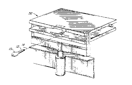
FIG. lA illustrates a perspective view of the key
retaining fixture of the electronic key identifier shown in
the "open" or key loading position.
FIG. lB illustrates a perspective view of the key
retaining fixture of the electronic key identifier shown in
the "closed" or key identification position.
66822-363

2 ~ 7~7~2
FIG. lC represents an enlarged sectional view of the
key retaining fixture illustrated in FIG. lB taken along
section lines lC-lC.
FIG. 2 illustrates an enlarged perspective view of
an unknown key blank inserted between first and second
Gurface segment sensors.
FIG. 3A represents a partially cutaway elevational
view of the structure illustrated in FIG. 2, taken along
section line 3A-3A.
FIG. 3B illustrates the key and first and second
sensor segments illustrated in FIG. 3A with the key
retaining fixture displayed into the "closed" or key
identification configuration.
FIG. 4A represents an enlarged elevational view of a
single surface segment sensor.
FIG. 4B represents an enlarged elevational view of a
pair of surface segment sensors to provide enhanced
resolution.
FIG. 5A illustrates a sectional view of an unknown
key blade together with the representative key blade
electronic images.
FIG. 5B illustrates a sectional view of a second
unknown key blade configuration and the different
electronic images relating to that different key blade
configuration.
FIG. 6A illustrates a third unknown key blank cross
sectional configuration.
FIG. 6B illustrates the electronic images
corresponding to the two sides of the key blade cross

~ 27~7~2
section depicted in FIG. 6A.
FIG. 6C illustrates database searching operations
for the purpose of identifying a correspondence between
the FI~ 6B electronic image and a stored electronic
image corresponding to a known key blank blade
configuration.
FIG. 7 illustrates a computer cathode ray tube
display of a group of known key blank shapes for
allowing a system operator to perform the final
selection or matching step between the shape of the
unknown key and a specific known key blank within the
displaced group.
DES~RIPTION OF THE PREEERRED EMR~DIMENT
In order to better illustrate the advantages of the
invention and its contributions to the art, a preferred
hardware ~rho~;rent of the invention will now be
described in detail.
Referring to FIGS. lA, lB, 2, 3A and 3B, an unknown
key 10 includes a key blade 12 formed from an
electrically conductive material such as brass. Key
blade 12 extends along a longitudinal axis 14 and
includes first and second parallel, spaced-apart side
surfaces 16 and 18. Each side surface 16, 18 is defined
by one or more collinear surface segments 20 each having
a defined length and a defined position relative to
longitudinal axis 14.
Each side surface 16, 18 also includes one or more
recessed segments 22 offset from side surfaces 16, 18.
Recessed segments 22 separate adjacent surface segments
20.
Referring now to FIGS. 2, 3, 4 and 5, the electronic

21 7~792
key identifier of the present invention includes first
and second surface segment sensors 24 and 26 each of
which includes a flat sensor surface 28. Bach surface
segment sensor 24, 26 includes a series of parallel,
spaced-apart electrical conductors 30 extending at
equal, spaced-apart intervals across the full width of
each segment sensor. In the preferred embodiment of the
invention, an elastomeric connector manufactured by
Advanced Connector Technology (.640 x .190 x .138 AD50)
has been found to work in a highly satisfactory manner.
Connectors of this type are frequently used in watches
and computers to interconnect a liquid crystal display
with related ~lectronic circuitry. In the preferred
embodiment of the invention illustrated in FIG. 2, a
spacing of 0.10 inches is provided between adjacent
electrical conductors. Adjacent conductors 30 are
separated by an elastomeric, silicon-based material
which serves as a resilient electrical insulator.
As illustrated in FIGS. 2 and 3, when key retaining
fixture 32 as illustrated in FIG. 1 is moved from the
~loading" position illustrated in FIGS. lA, 2 and 3A
into the ~closed~ or key identification position shown
in FIGS. lB and 3B, sensor surfaces 28 and electrical
conductors 30 are brought into physical and electrical
contact with surface segments 20 of sides 16, 18 of key
blade 12 but are not brought into either physical or
electrical contact with recessed segments 22.
FIG. 4A illustrates how surface segment sensors 24,
26 are electrically interfaced with the conductors 34 of
an adjacent printed circuit board. As illustrated in
FIG. 4A, printed circuit board conductors 34 are spaced
apart by 0.01 inches to interface with conductors 30
:which are spaced apart by a distance of 0.002 inches.
The intervening insulating material 36 is clearly
illustrated in FIG. 4A.

~ ~ ~ 7~7q2
In one embodiment of the invention, a fixed voltage
such as five volts is applied to each conductor 34 so
that as illustrated in FIG. 3B, establishing physical
contact between conductors 30 of surface segment sensors
24, 26 and surface segments 20 of the electrically
grounded key blade 12 will direct a flow of electrical
current through each sensor conductor 30 in contact with
each surface segment 20.
FIG-S. 5A and 5B illustrate how using techniques well
known to those of ordinary skill in the art, a flow of
electrical current through designated conductors 30 can
be electrically converted into pixels or data as
illustrated by rectangular image segments 38 in FIGS. 5A
and 5B. Such data essentially generates an electronic
image designating the length and position of each
surface segment 20 of the blade 12 of an unknown key.
In FIGS. 5A and 5B, the vertically oriented dotted lines
illustrate the relationship between electronic segments
38 and the m-echanical configuration of surface segments
20 of the unknown key. The gaps between adjacent
electronic segments 38 essentially define the length and
position of recessed segments 22.
The electronic image segments 38 illustrated above
key blade 12 in FIG. 5A demonstrate the correspondence
between that electronic image of the first and second
sides 16, 18 of key blade 12 and the mechanical
structure of that key blade. Similar representations
appear in FIG. 5B and in FIGS. 6A/6B.
FIG. 6C illustrates the sequential electronic key
identification process of the present invention. FIG.
6A illustrates the cross sectional geometry of the
surface~segments 20 and the recessed segments 22 of
blade 12 of an unknown key. FIG. 6s illustrates the
electronic image corresponding to the key blade
illustrated in FIG. 6A. FIG. 6C symbolically represents

~ 2 ~ 7~792
a comprehensive database of electronic images of the
first and second sides of a variety of key blades
corresponding to known key designs. Using programming
techniques well known to those of ordinary skill in the
art, computer software is prepared to implement the
image matching process illustrated in FIG. 6. Using
such data processing techniques, the image of the
unknown key blade illustrated in FIG. 6B is
electronically matched with corresponding known image 40
~as shown in FIG. 6C. Data corresponding to that matched
key blank can then be displayed to an operator through a
variety of well known computer-based display means such
as a cathode ray tube, a digital readout or similar
me~h;ln; ~m~
In certain instances, identification of a one to one
corresponding between the geometry of an unknown key
blade and the image of a known key blade will provide a
certain degree of ambiguity as illustrated in FIG. 7.
In certain unique situations, a single key blade
geometry may appear on a significant variety of unknown
keys having a variety of unknown key shapes as
illustrated in FIG. 7. In the example shown, nine
different unknown key shapes may correspond to three
different functionally compatible (although
geometrically dissimilar~ key blanks. As illustrated in
FIG. 7, a single identified key blade side surface
geometry corresponds to nine different key styles and to
potentially compatible key blank numbers 66, 67 and 70.
When implementation of the electronic key
identification process of the present invention results
in the identification of a group of known key blanks as
illustrated in FIG. 7 rather than a single key blank, an
additional step is required. When group matching
occurs, as illustrated in FIG. 7, the computer cathode
ray tube will display an image substantially as
illustrated in FIG. 7 to allow the operator to visually

~ 2~7g7~2
match the shape of the unknown key sought to be
duplicated with the shape of a limited number of
potential key blank candidates. Once a one to one
correspondence between the shape of the unknown key
blank and the shape of a depicted key blank has been
obtained, the operator is immediately able to determine
the number of or other identi~ier for a single
functionally compatible (althoug~ not necessarily
geometrically identical) key blank. Utilization of that
functionally compatible key blank will allow the
operator to successfully duplicate the bit notch pattern
of the unknown key on that functionally compatible key
blank and will allow the customer to obtain a key which
will be functionally compatible with the customer~s
lock.
In certain instances, it may be desirable to enhance
the resolution of data relating to the length and
position of surface segm-ents 20 of the unknown key to
provlde for enhanced computer-based matching. As
illustrated in FIG. 4B, a two-fold resolution
enhancement can be achieved by formins a single surface
segment sensor 24 from a pair of sensor elements 42 and
44. In the FIG. 4B embodiment of the invention, the
resolution is increased by a factor of two from 0.10
inches as available with the FIG. 4A embodiment to a
resolution of 0.005 inches as illustrated in FIGS. 4B.
As illustrated in FIG. lC, key retaining fixture 32
includes a key receiving receptacle 46 including funnel-
shaped side surfaces and a narrow keyway 48 which
assists in obtaining appropriate longitudinal alignment
of key 10 such that longitudinal axis 14 of key 10 is
oriented approximately parallel to the orientation of
conductors 30 of surface segment sensors 24, 26.
While the electronic key identifier of the present
invention has been disclosed as utilizing a surface

2 ~ ~8792
segment sensor having a plurality of electrical
conductors 30 which physically contact raised surface
segments 20 of an unknown key, a capacitor or other
eguivalent surface proximity sensing means could be
utilized to sense the proximity of the ~urface segments
20 to the surface segment sensors and the spaced apart
relationship between the sensors and recessed segments
22. Accordingly, it is intended.by the appended claims
to cover all such modifications of ~he invention which
fall within the true spirit and scope of the invention.

Representative Drawing
A single figure which represents the drawing illustrating the invention.
Administrative Status

2024-08-01:As part of the Next Generation Patents (NGP) transition, the Canadian Patents Database (CPD) now contains a more detailed Event History, which replicates the Event Log of our new back-office solution.

Please note that "Inactive:" events refers to events no longer in use in our new back-office solution.

For a clearer understanding of the status of the application/patent presented on this page, the site Disclaimer , as well as the definitions for Patent , Event History , Maintenance Fee  and Payment History  should be consulted.

Event History

Description Date
Inactive: Expired (new Act pat) 2016-06-11
Inactive: IPC from MCD 2006-03-12
Inactive: Late MF processed 2004-08-20
Letter Sent 2004-06-11
Grant by Issuance 1999-07-06
Inactive: Cover page published 1999-07-05
Pre-grant 1999-03-26
Inactive: Final fee received 1999-03-26
Letter Sent 1999-02-18
Amendment After Allowance Requirements Determined Compliant 1999-02-18
Amendment After Allowance (AAA) Received 1999-01-21
Letter Sent 1998-09-29
Notice of Allowance is Issued 1998-09-29
Inactive: Application prosecuted on TS as of Log entry date 1998-09-22
Inactive: Status info is complete as of Log entry date 1998-09-22
Inactive: Approved for allowance (AFA) 1998-08-20
Letter Sent 1998-07-06
Reinstatement Requirements Deemed Compliant for All Abandonment Reasons 1998-06-17
Deemed Abandoned - Failure to Respond to Maintenance Fee Notice 1998-06-11
Application Published (Open to Public Inspection) 1997-05-01
Request for Examination Requirements Determined Compliant 1996-11-08
All Requirements for Examination Determined Compliant 1996-11-08

Abandonment History

Abandonment Date Reason Reinstatement Date
1998-06-11

Maintenance Fee

The last payment was received on 1999-05-20

Note : If the full payment has not been received on or before the date indicated, a further fee may be required which may be one of the following

  • the reinstatement fee;
  • the late payment fee; or
  • additional fee to reverse deemed expiry.

Patent fees are adjusted on the 1st of January every year. The amounts above are the current amounts if received by December 31 of the current year.
Please refer to the CIPO Patent Fees web page to see all current fee amounts.

Owners on Record

Note: Records showing the ownership history in alphabetical order.

Current Owners on Record
THE HILLMAN GROUP, INC.
Past Owners on Record
BRADLEY DEE CARLSON
JEFFREY CLARK HEIDEL
WARREN WAYNE STANSBERRY
Past Owners that do not appear in the "Owners on Record" listing will appear in other documentation within the application.
Documents

To view selected files, please enter reCAPTCHA code :


To view images, click a link in the Document Description column. To download the documents, select one or more checkboxes in the first column and then click the "Download Selected in PDF format (Zip Archive)" or the "Download Selected as Single PDF" button.

List of published and non-published patent-specific documents on the CPD .

If you have any difficulty accessing content, you can call the Client Service Centre at 1-866-997-1936 or send them an e-mail at CIPO Client Service Centre.


Document
Description 
Date
(yyyy-mm-dd) 
Number of pages   Size of Image (KB) 
Abstract 1996-09-22 1 24
Description 1996-09-22 10 389
Claims 1996-09-22 9 252
Drawings 1996-09-22 5 198
Description 1999-01-20 11 434
Representative drawing 1999-06-28 1 18
Representative drawing 1997-10-27 1 45
Reminder of maintenance fee due 1998-02-11 1 111
Courtesy - Abandonment Letter (Maintenance Fee) 1998-07-05 1 189
Notice of Reinstatement 1998-07-05 1 172
Commissioner's Notice - Application Found Allowable 1998-09-28 1 163
Maintenance Fee Notice 2004-08-08 1 172
Late Payment Acknowledgement 2004-09-12 1 166
Correspondence 1999-03-25 1 39
Correspondence 2006-10-18 1 9
Correspondence 1996-11-07 1 45