Note: Descriptions are shown in the official language in which they were submitted.
WO 95/17014 ~ '~ '' 217 9 d 5 2 P~~594I14335
_1_
INTEGRATED SILICON VACUUM MICROPACKAGE
FOR INFRARED DEVICES
This application relates to the field of infrared sensing and infrared scene
projection or emission, and particularly to the packaging of arrays of small
elements
thereof.
Thermal isolation is very important for thermal based infrared devices
(detector
or emitters), as opposed to quantum sensors or emitters, since the detection
or
transmission of infrared radiation is directly related to the temperature rise
achieved by
the detector or emitters of the device. The better the thermal isolation of
the detector or
emitters the more effcient the device will be at converting radiation to heat
(detector) or
heat to radiation (emitter). Vacuum packaging is a very effective means to
improve
performance. It reduces heat flow from individual infrared units to their
neighbors
and/or to surrounding surfaces via ambient gas molecules by eliminating such
molecules.
Because microstructure infrared detector and emitter arrays are very small and
fragile, common silicon production and packaging techniques may not be
suitable for
large scale production of these array bearing devices. Typical infrared units
in the
arrays are built to be thermally isolated from the chip, as well as their
neighbors, thus
having elements suspended apart from the substrate to enhance the thermal
isolation by
having the minimal physical contacts possible. These bridges or suspension
structures
can be particularly fragile, therefore the method of encapsulating them into a
vacuum
can be critical to device yield rates.
A method for packaging the die in a batch process substantially improves the
yield, reduces the cost and at the same time achieves maximum performance of
these
devices. This type of packaging is necessary to mass produce low cost,
thermally based
infrared devices. The proposed package is termed a "micropackage."
Maintaining an effective vacuum in a sealed package is often challenging due
to
surface outgassing. Frequently heat treatments will minimize this but such
outgassing
determines the effective life of the device unless it can be periodically or
continuously
removed. Integrating a getter into each discrete chip would be a method of
maintaining a
good vacuum for all chips as the getter will counteract the outgassing
generated by the
package surfaces.
WO 95117DI4 21 ~ 9 ~ ~ 2 PCT/US94114335
_._ _2
The innovative structures taught here provide tremendous cost savings over
prior
designs for packaging these devices, the capability of achieving much smaller
packages,
as well as having the potential to greatly increase packaged device yield for
lower cost.
Fig. 1 is a plan view of a wafer level design employed by a preferred
embodiment of the invention.
Fig. 2 is a cut-away side view at the wafer level in accord with a preferred
embodiment of the invention.
Fig. 3 is a cut-away side view of an individual device of one preferred
embodiment chip of the invention.
Fig. 4 is a cut-away side view of another preferred embodiment chip of the
invention.
Fig. 5 is side view of two major components at the chip level of a preferred
embodiment of the invention.
Fig. 6 is a top view of the surface patterning of the substrate layer (upper
surface) at the chip level of a preferred embodiment of the invention.
A construction technique and infrared device built thereby are described
herein.
A wafer assembly having infrared devices (which can be detectors or emitters,
either singly or in an array or arrays) provide for an inexpensive way of
packaging
infrared devices. The wafer is covered and maintained in a vacuum by a top cap
of
infrared transparent material spaced apart therefrom by a solder bead and
farther from
the structure of the top cap wafer in some instances.
In either case, the result is a minimally thermoconductive space between the
top
cap and the infrared devices, which can be evacuated or filled with minimally
thermoconductive fluid. The spacing can be provided by any or all of the
solder bead; a
recess in the top cap or an additional spacer layer of material added either
to the bottom
of the top cap or the upper surface of the infrared containing wafer.
In the preferred embodiment, the wafer assembly is then diced into its final
chip
components, each maintaining individual vacuum integrity. It is preferred that
each
vacuum cavity have an integral getter to increase the vacuum life of the
component.
CA 02179052 2000-06-20
64159-1453
2a
In accordance with the present invention, there is
provided an infrared sensitive package, having a substrate (9)
having an inner and outer surface, and infrared detector
elements (20) on the inner surface of said substrate,
characterized by: a top cover (12) of infrared transparent
material in spaced relation to the inner surface of said
substrate (9), sealing means (16) between said top cover (12)
and the inner surface of said substrate (9), whereby an
atmosphere of low thermal conductivity is maintained over said
infrared detector elements (20).
In accordance with the present invention, there is
further provided an infrared emitting package, having a
substrate (9) having an inner and outer surface, and infrared
emitting elements (20) on the inner surface of said substrate,
characterized by: a top cover (12) of infrared transparent
material in spaced relation to the inner surface of said
substrate (9), sealing means (16) between said top cover (12)
and the inner surface of said substrate (9), whereby an
atmosphere of low thermal conductivity is maintained over said
infrared emitting elements (20).
In accordance with the present invention, there is
further provided a process of making infrared array packages,
having an array in infrared elements therein, comprising: a)
evacuating a chamber containing a infrared array carrying
substrate (9) and a infrared transparent top cap (12) having
thereon a sealing means (16), b) contacting said substrate (9)
to said sealing means (16) on said top cap (12) to provide a
sealed cavity between said infrared carrying substrate (9) and
said top cap (12), c) activating said sealing means (16) to
provide a permanent seal between said infrared carrying
substrate (9), and said top cap (12).
W0 95/17014
2 l l 9 0 5 2 PCT/US94/I4335
-3-
DETAILED DESCRIPTION OF THF PREFER_RF.D EMBODIMENT
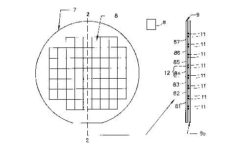
Referring first to Fig. 1, a wafer which will be used to create a set of
devices in
accord with a preferred embodiment of the invention is shown, being a wafer
composed
of many devices or chips 8, constructed thereon by prior processes not
described here.
In Fig. 2, a cross-sectional view is taken of a wafer like 7 of Fig. 1, having
a top
cap wafer (9b) attached thereto. The top cap wafer (9b) should be an IR
transparent
wafer. When attached in a vacuum, all the devices on one wafer are
simultaneous
sealed by the cap, in a highly efficient batch fabrication technique. The
spacer material
11 both holds the wafers 9 and 9b apart and seals each individual chip or die
8, in its
own area. The dotted lines around 84 show where the paired wafers would be
diced to
produce a chip based on the infrared device in area 84
Referring now to Fig. 3, a device in accord with the preferred embodiment 10
is
illustrated at the "device" or chip level, having two major component parts; a
substrate
or base chip 9 and a top cover 12. On the surface of the top cover 12 is an
anti-
reflective layer 13 and underneath its surface is a second anti reflective
coating 14.
(Substances used for anti-reflective coatings are well known.) The joining of
the two
halves in accord with this invention yields a space 21 between them. By
sealing them
together, preferably with a solder layer 16, 16a while the two halves are in a
vacuum,
the cavity 21 itself remains evacuated. The solder layer can be applied by
vacuum
deposition and either lift-off or etch, or by masking and plating. The wafer
or chip
containing the microbolometers 20 and or other type (pyroelectric,
thermoelectric, etc.)
of thermal infrared sensitive devices, are manufactured first. Such
manufacture is not a
part of this patent and can be done in numerous known ways. There can be
electronics
beneath the surface layer that provides some signal processing and/or
switching
25 properties which the infrared sensitive devices (20) will use. Generally,
there is a layer
22 of electrical connections and the microbolometer 22a or other infrared
sensitive or
emitting devices. These electrical leads can be passivated (i.e., coated with
a protective
layer of material, for example, silicon nitride or other well known
passivation material)
such that the solder layer can be applied over them and form the vacuum seal
without
shorting the leads together. The leads terminate on pads 18 that wire bonds
can be made
on and connected to other circuitry off the infrared sensitive device.
kC~~'. tY)'yEYyNI.E:!(.'Ht\ Uo ...,.-.. ' 1~-'.'L~': a5 : G.'.~13 ~_......~-
61'- X51 GEpf-J- _.__ '"1'J' k3J -3J~J~~(:.:~X 3
___ _ .. _ ~.,~~ . . . _.
i::~..
-' ~ 17952
-4-
The infrared sensitive elements 20 are usually thin film structures that are
suspended above the chip surface for thermal isolation and such devices are
very fragile
in subsequent manufacturing steps. Figure 3 illustrates devices where this
thermal
isolation is accomplished by etching away part of the substrate 22b. The top
cap needs
to be separated from the thermally isolated elements so as to not touch isle
elements and
conduct heat towards or away from the elements. An effective way to assure a
good
cavity size is tn etch a recess in the top cap surface 15. W"ith this etching
done, when
the solder is molten and the wafers arc pressed together, e:ctreme measures
are not
necessary to prevent the solder from being squeezed out. causing the
separation berivcen
F O pads I Sa and 16 could become extremely' small where the top cap it etched
back, even
with poor processing the cavity will be maintained. A metal layer I ~a Ehat
the solder
can wet to and to allow for the solder 16, 16a to be patterned on the top cap
sttrfacc so
as to form a ring or frame large enough to encircle the array of thermally
isolated
structures ~0. A similar ring or frame of metal that the solder can wet to may
also be
1~ preferably created on the wafer of detecior,~emitter die.
Two wafers are brought together in vacuum, using suitable wafer bonding
equipment. Low levels of heat may be used for this processing step ( solder
usually
refiows between 100-300 °C depending on type used, w~e presently prefer
to use 50;50
InPb. The user tnay, of course, use any solder he/she profess.} The die are
sealed in
20 vacuum and the fragile thermally isolated elements err protected from
damage and
debris associated with subsequent wafer sawing and die handling b,' the
surrounding
solder bead. Lines for wafer sawing 27, illustrate in one direction how die
would be
separated while maintaining the inmgrity of soidvr seal. (The cop cap 1?
should also
have had its anti rellective layers 13 and 14 placed thereon before the
joining of the two
25 halves 12 and 9.)
Because the resultant package is only the thickness of bNO silicon wafers the
result is a significant reduction in bet<'t the size and the weight of the
package as
compared to a standard vacuum packa~t far similar devices. This aspect is
important
and desirable for almost all applications of infrared devices,
30 To ensure a low pressure is mairt~ined within a micropacka=a (chin level
vacuum cavity 21), it is useful to ensure that nn materials which will
excessively outgas
lie within the tnicropackage. In addition, .since the internal sut~:ces of the
infrared die
''.'c;:.;r J ;;-~_T
i ~i.
PCT/US94/14335
wo 95~1~014 217 9 0 5 2
1
-5-
and overlying window or top cap will have at least a small outgassing rate, it
may be
necessary, or at least useful, to include small quantities of a specialized
getter material
within the micropackage. The function of the getter material is to absorb
outgassants,
which would otherwise cause an increase in the internal pressure of the
micropackage
and the resulting decrease of the thermal isolation of the IR detector or
emitter elements.
Suitable getter materials are well known, such as thin films of barium,
vanadium,
iron, zirconium or their alloys. Before such materials can act as getters,
they must be
activated by heating to a high temperature for a short period.
To incorporate and activate small quantities of getter materials within a
micropackage, the required mass of getter material may be deposited
monolithically
upon suitable regions of the infrared die or the top cap. Numerals 23 and 24
show
locations where such monolithic getters may preferably be placed. The getter
material
may be either deposited directly upon these surfaces 24, or upon thermally
isolated
. microbridges 23 of such materials as silicon nitride. An advantage of
deposition upon a
microbridge is that the thermal isolation property of the microbridge allows
thermal
activation of the getter material by a small heating power applied for a short
time, for
example by an electrical heating current or a beam of heating radiation as
produced by
an infrared laser, without requiring the adjacent parts of the infrared die or
window to be
heated significantly.
If the getter is on a thermally isolated structure, an alternate heating
method may
be the supply of an electric current passed through a resistive heating
element fabricated
on the structure to heat the structure enough to activate the getter. To get
electric power
to the heater another solder pattern 23c can be produced at the same time as
the solder
ring 16, 16a to connect pads on the top oap 23a to pads on the device chip
23b. These
pads 23b consist of a metal that solder can wet to and connect to leads 22
which will
connect to pads 18 for wire bonding. A hole through the wafer 26 over the pads
allows
access to the sealed devices for wirebonding. If desired, a large molecule or
atomic gas,
preferably non-reactive such as Xenon, maybe used instead of the vacuum or
vacuum/getter filler. Xenon is known, for example, to be only one-fifth as
thermally
conductive as air. Currently, the evacuated space and getter combination is
preferred,
however.
2179052
w0 95/17014 PCTIUS94/14335
_6_
For lowest cost the top cap 12 should preferably be comprised of single
crystal
silicon, with low absorption in the region of infrared detection or emission.
This is
material which is transparent to infrared radiation and easily obtainable.
Alternatively
a window in the top cap wafer, or the top cap wafer itself, could be formed of
a thin film
of polycrystalline silicon or other materials such as germanium, GaAs, etc.
with
different degrees of transparency. Thus, if the structures at 20 are emitting
structures,
the infrared can be transmitted through the top cap 12 and, if they are
receiving or
detector structures, the infrared from the environment can be received into
them also
through top cap 12.
Referring now to Fig. 4, a substrate with infrared sensitive devices 44 is
indicated by the numeral 41 and the device overall by the numeral 40. For very
large
arrays of infrared sensitive devices or thin windows in the top cap, the load
of
atmospheric pressure on the top cap and device chip can cause bowing such that
the two
inner surfaces can touch. At least one support post 43 may be added to cause
the top
cap to remain separated from the top cap 42 which in this embodiment is
lengthened
substantially without increasing its width. This permits for the encapsulation
of very
large arrays or infrared sensitive structures which are substantially more
useful in
infrared imaging devices, such as cameras, for instance. Figure 4 also shows
another
method that the top cap can be spaced apart from the thermally isolated
elements. A
standoff 45 of deposited material such as a metal can be patterned at the same
time as
the support post 43 thereby eliminating the need for the recess etch in the
top cap
surface. If desired, a metal that the solder can wet to can be patterned on
top of the post
for subsequent soldering operations.
In another alternative the getter could be placed on a thermally isolated
structure
on the detector/emitter die 47. Electrical connections to this getter for
heating can be
made as in the structure depicted in figure 3 with layers such as 22 and pads
I 8.
To farther integrate the electronic portion of the system, electronic devices
48
could be fabricated in the top cap wafer and connections can be made to these
devices in
the same manner as the thermally isolated getter in figure 3 with pads 23a,
23b, solder
23c. Some of the benefits of placing electronics in the top cap are further
size reduction,
lower electrical noise due to shorter leads, and temperature matched very
closely to the
infrared sensitive die.
.,
WO 95/17014
. ~ ~ ~ 7 q 0 ~ 2 FGT/US94/14335
A layer of solder is preferable to all other structures known f~:r this kind
of
bonding in a vacuum environment. However, ultrasonic pressure devices may also
be
used if properly constructed to push the entire post or pedestal structure
against the
surface of substrate 41 all at the same time.
A simple representation of the structure 30 is found in Fig. 5. In this case,
a gap
or hole 33 is made (in this case by etching) to provide for direct access to
the bonding
pads so that the infrared structures in substrate 31 (not shown) can have
electrical access
to the outside world. A layer of solder 34 is shown located on the underside
of top cap
32 showing where such a solder layer might be located in a cold form for one
preferred
form of assembly.
Referring now to Fig. 6, the areas 51 through 59d of interest are illustrated
on a
surface 31. In the center of the set of structures is the area 51 in which the
infrared
sensitive structures would be located. Area 52 indicates the region in which
the top cap
cavity edge would be located. Beyond this is area 53 in which the solder layer
such as
that shown in Fig. 5 (numeral 34) would be located. The outer edge 54 is also
shown.
Wire bonding pads 58a through 59d are shown within area 54. Area 55 describes
the
opening 33 as it may be situated when wafers or dies 31 and 32 are brought
together for
bonding. Thus, the bonding pads 58a through 59d would be available through
opening
33.