Note: Descriptions are shown in the official language in which they were submitted.
2179088
SPECIFICATION
PIEZOELECTRIC ACOUSTIC DEVICE
BACKGROUND OF THE INVENTION
1. Field of the Invention:
The present invention relates to a piezoelectric acoustic device
having a piezoelectric element adapted for use in an acoustic device such
as a receiver of a telephone, etc.
2. Prior Art:
A conventional piezoelect~ic acoustic device comprises a case like a
tray for accommodating piezoelectric element therein, a stepped
piezoelectric element support provided at an inner peripheral side of the
case at the intermediate portion thereof, wherein a peripheral portion of a
diaphragm is placed on and fixed to the piezoelectric element support by
an adhesive. In the piezoelectric element, one of electrodes provided on
both surfaces of a plate-shaped piezoelectric body is bonded to a surface of
the diaphragm wherein lead wires are respectively connected to the
electrode on the piezoelectric element and the diaphragm and are
extended outside from the case.
Such a piezoelectric acoustic device is incorporated into an
electronic device such as a portable telephone, a so-called cordless phone,
then it is fixed to the housing by screws, etc. Further, the lead wires are
connected to a printed circuit board in the housing by soldering, etc.
In addition to the piezoelectric acoustic device connected by the lead
wires, there is a piezoelectric acoustic device having no lead wires
wherein conductive pins provided in the case contact the diaphragm and
the electrodes of the piezoelectric element so as to connect to the circuit.
- ` 2l7snss
This piezoelectric acoustic device is also accommodated in the housing of
the electronic device and is fixed to the housing by screws, etc.
However, in the aforementioned piezoelectric acoustic devices,
since the case attaching the piezoelectric element thereto is employed,
parts count is increased, steps of assembly are increased, so that the
manufacturing cost can not be reduced and the miniaturization of the
device is difficult. When the case is fixed to the housing, lead wires must
be soldered, which took however much time and labor.
SUMMARY OF THE INVENTION
In view of the drawbacks of the conventional piezoelectric ~coustic
device, it is an object of the invention to provide a piezoelectric acoustic
device in which a piezoelectric element is easily fixed to an electronic
device, and is connected to a circuit without taking time and labor so that
it can be manufactured with low cost and can be miniaturized.
Accordingly, the electronic device can be easily assembled.
To achieve the above object, in the present invention, a projection is
provided on a periphery of a metallic plate-shaped diaphragm of a
piezoelectric element, and an extension electrode electrically extended
onto a main surface of the projection wherein the extension electrode is
electrically connected to the diaphragm of a plate-shaped piezoelectric
body while allowing the extension electrode to be insulated from the
diaphragm. The piezoelectric element is directly fixed to a housing, and
the extension electrode and the projection are electrically connected to
circuit patterns on the printed circuit board which is accommodated in a
housing of an electronic device by way of conductive portions of an elastic
connection block.
A piezoelectric acoustic device comprises a piezoelectric element
composed of a metallic plate-shaped diaphragm, a plate-shaped
2l7snss
piezoelectric body, electrodes provided on both main surfaces of the
piezoelectric body, one electrode being fixed and electrically connected to a
main surface of the diaphragm, and a casing for accommodating the
piezoelectric element therein and forming a resonant chamber together
with the piezoelectric body. The piezoelectric element further comprises a
projection projecting from the diaphragm and an extension electrode, the
extension electrode being extended onto the projection while being
insulated from the diaphragm, the extension electrode being electrically
connected to another electrode which is not fixed to the diaphragm of the
piezoelectric body, the piezoelectric element being attached to the casing
while allowing a main surface of the projection attaching the e~tension
electrode thereto to direct outward. Further, a metallic surface portion of
the projection and the extension electrode are respectively electrically
connected to circult patterns of a printed circuit board mounted inside the
housing by way of conductive portions provided on an elastic connection
block. Accordingly, the device can be miniaturized, and simplified in the
structure thereof, and further easily connected to the circuit. In this
case, the connection block is clamped between the projection supported by
an electrode supporting portion of the housing and the printed circuit
board 36 while compression stress is given therebetween.
The connection block is an elastic block having a plurality of
conductive portions provided at least on the surface thereof, wherein the
conductive portions are arranged alternately in a given interval while
being insulated therebetween. The housing includes a holding means for
holding the connection block for temporarily fix the connection block
thereto when the piezoelectric acoustic device is incorporated into the
housing of the electronic device.
Further, the housing includes a sound damper.
2l7snss
\ -
In the aforementioned piezoelectric acoustic device, the extension
electrode provided on the projection of the diaphragm and the surface of
the projection are connected to the circuit patterns of the printed circuit
board using the elastic connection block, which dispenses v~ith soldering
of the lead wires. Since the piezoelectric element is directly attached to the
inside of the housing of the electronic device, it is not necessary to attach
the piezoelectlic element to the housing and to fix the housing by screws
etc. That is, the connection block is clamped between the projection
supported by the electrode supporting portion of the housing and the
printed circuit board while compression stress is given therebetween and
the connection between the piezoelectric element and the circuit of the
printed circuit board is completed by merely attaching the piezoelectric
element to the inside of the housing and fixing the housing in a given
condition.
Since the connection block is elastic block having a plurality of
conductive portions which are provided at least on the surface thereof and
are arranged alternately in a given interval while being insulated
therebetween, when the connection block is clamped between the
projection supported by the electrode supporting portion of the housing
and the printed circuit board while compression stress is given
therebetween, the diaphragm and the electrodes of the piezoelectric body
can be easily connected to the circuit patterns of the plinted circuit board.
Particularly, if the housing includes a holding means for holding the
connection block, when the piezoelectric acoustic device is incorporated
into the housing of the electronic device, the connection block can be
temporarily fixed to the housing, which enhances the incorporation of the
piezoelectric acoustic device into the housing. Further, since the housing
includes a sound damper, the piezoelectric acoustic device can attain
2179088
.
excellent acoustic characteristics although it has a small size and a
simple structure.
BRIEF DESCRIPTION OF THE DRAWINGS
Fig. l(a) is an exploded longitudinal cross-sectional side view of a
piezoelectric acoustic device when it is disassembled according to a first
embodiment of the invention;
Fig. l(b) is a longitudinal cross-sectional side view of the
piezoelectric acoustic device when it is assembled;
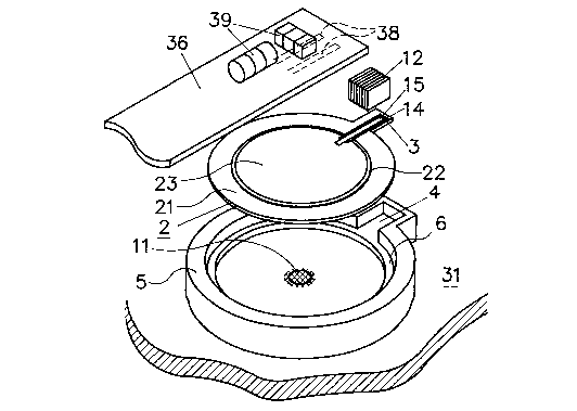
Fig. 2 is an exploded perspective view of an electric device employed
by the piezoelectric acoustic device of Fig. 1 removing a shell member of a
housing thereof;
Fig. 3 is a plan view showing a state where the piezoelectric element
is attached to the other shell member of the piezoelectlic acoustic device of
the first embodiment;
Fig. 4 is an exploded perspective view showing a main portion of the
electric device employing the piezoelectric acoustic device of Fig. 1
removing one housing thereof;
Fig. 5 is a plan view showing a state where a main portion of the
piezoelectric element is attached to the shell member of the piezoelectric
acoustic device of the first embodiment;
Figs. 6(a) and 6(b) are plan views showing main portions of
projections of diaphragms of the piezoelectric acoustic device according to
a modification of the first embodiinent of the invention;
Figs. 7(a) and 7(b) are plan views showing main portions of
electrode supporting portions of the housing of the piezoelectric acoustic
device according to a modification of the first embodiment;
2179088
Fig. 8 is an exploded perspective view showing another example of a
main portion of a temporary fixing means for fixing a connection block to
the projection of the diaphragm; and
Fig. 9 is an exploded perspective yiew showing a still another
example of a main portion of a temporary fixing means for fixing the
connection block to the projection of the diaphragm;
PREF'ERRED EMBODIMENT OF THE INVENTION
A preferred embodiment of the invention will be now described in
detail with reference to attached drawings.
First Embodiment (Fig. 1 through Fig. 9): -
Figs. 1 through 5 sho~,v a first embodiment which applies theinvention to a piezoelectric receiver. A housing 1 of an electronic device
such as a portable phone, a cordless phone, etc. comprises a pair of shell
members 31 and 37 made of resins, etc. wherein these shell members 31
and 37 are overlaid on each other and fixed to each other using screws,
etc., not shown, thereby forming a space therein for accommodating an
electronic device.
As shown in Figs. 2 through 4, a peripheral wall 5 is fomred in the
inner surface of one shell member 31, and a sound damper 11 comprises
a hole which is bored at the central bottom part surrounded by the
peripheral wall 5 and is covered with a mesh made of Tetoron
(trademark) having about #380 meshes. The sound damper 11 can select
a suitable shape of various shapes depending on acoustic characteristics
to be obtained, for example, it can be formed of a plurality of small sound
emitting holes.
An electrode supporting portion 4 projects from a part of the
peripheral wall 5. The electrode supporting portion 4 is like a groove
having inner dimensions corresponding to the dimensions of a projection
2l7~nss
' -
3 which projects radially fronl a peripheral portion of a diaphragm 21 of a
piezoelectric element 2, described later.
The electrode supporting portion 4 projects radially from an outer
peripheral portion of the housing 1. A step 6 is formed on an inner
peripheral wall 5 of the housing 1 at the middle portion thereof in the
direction of the inner height of the pelipheral wall 5 and extends along the
entire periphery of the housing 1 excepting the electrode supporting
portion 4 for supporting the peripheral portion of the diaphragm 21 of the
piezoelectric element 2.
As shown in Figs. 2 through 5, the piezoelectric element 2
comprises a plate-shaped piezoelectric body 22 made of piez~electric
ceramics, etc., and electrodes 23 provided on both main surfaces of the
piezoelectric body 22 (only one of the electrodes 23 is seen and illustrated in
Fig. 2. through 5). One of the electrodes 23 of the piezoelectric body 22 is
fixed and electrically connected to the metallic diaphragm 21. The
diaphragm 21 and the piezoelectlic body 22 of the piezoelectric element 2
are respectively circular. A diameter of the diaphragm 21 of the
piezoelectric element 2 is slightly greater than an inner diameter of the
step 6 of the housing 1, and is slightly less than an inner diameter of the
peripheral wall 6 at the upper portion of the step 6.
As shown in Figs. 1 through 5, the projection 3 projects from the
peripheral portion of the diaphragm 21 and also projects radially, i. e. in a
direction of the radius of the diaphragm 21. A belt-shaped insulating
layer 14 is formed to extend from the electrodes 23 of the piezoelectric body
22 to the projection 3. A belt-shaped extension electrode 15 composed of a
conductive film is formed on the insulating layer 14. The extension
electrode 15 extends over an edge of the end of the insulating layer 14 at
the side of the electrodes 23 of the piezoelectric body 22 wherein the end
portion of the extension electrode 15 contacts the electrodes 23 so that the
2179088
extension electrode 1~ is electrically connected to the electrodes 23. As
shown in Fig. 5, the insulating layer 14 and the extension electrode 15 are
respectively deflected on the projection 3, namely, formed at one side of the
projection 3, while the metallic surface of the projection 3 is exposed at the
other side of the projection 3. In Fig. 5, a width of the extension electrode
15 is denoted at B and a width of the portion of the projection 3 where the
metallic surface is exposed is denoted at B'. A margin between the edge
of the extension electrode 15 and that of the insulating layer 14 is denoted
atA.
Further, according to the piezoelectric acoustic device of this
embodiment, a connection block 12 shown in Figs. 4 and 5 is pr~pared.
The connection block 12 is a block as disclosed, e.g. in Japanese Patent
Publication No. 56-48951 or an elastic block which is commercially
available in the name of"INTERCONNECTOR", wherein insulating
portions 13 and conductive portions 16 are arranged alternately in a given
pitch at least on a surface of the elastic block 12. F'or example, the
connection block 12 is formed of a layered body in which elastic insulating
bodies and elastic conductive bodies each having a given thickness are
respectively alternately layered, or it is formed of an elastic block in which
a surface of the connection block 12 is metalized in a given interval like a
belt.
A width of the connection block 12 is slightly greater than the inner
dimensions of the electrode supporting portion 4 of the housing 1. Each
width of the insulating portions 13 is denoted at b and each width of the
conductive portions 16 is denoted at a. The following dimensional
relations or expressions are established between the extension electrode
15, the insulating layer 14, and the metallic surface of the projection 3.
A>a, B>b, B'>b.
2l7snss
To incorporate the piezoelectric element 2 having such an
arrangement into the housing 1, an adhesive such as a silicon adhesive is
uniformly coated previously on the step 6 within the inner periphery of the
peripheral wall 5 of the shell member 31 of the housing 1 provided with
the sound damper 11 which includes a damper means such as a meshed
damper cloth made of fluorine resin or a pin hole damper. Next, the
piezoelectric element 2 is accommodated inside the peripheral wall 5
while the piezoelectric body 22 is directed upward, and the peripheral
portion of the diaphragm 21 of the piezoelectric element 2 is placed on and
fixed to the step 6 by the adhesive. At this time, the pro3ection 3 is engaged
in the electrode supporting portion 4 of the shell member 31. - It is
possible to select a suitable shape and structure of the damper 11 among
various shapes and structure depending on the acoustic characteristics to
be obtained. In such a manner, the piezoelectric element 2 is attached to
the inner side of the peripheral wall 5 of the shell member 31.
Whereupon, a printed circuit board 36 is supported or held by a
board support portion 41 within the other shell member 37 constituting the
housing, wherein circuit patterns 38 and 38 (refer to Fig. 2) to be
connected to the diaphragm 21 and the electrodes 23 of the piezoelectric
element 2 are provided on the lower surface of the plinted circuit board 36
in Fig. 1. In Fig. 1, denoted at 39 is a circuit component mounted on the
printed circuit board 36 and it constitutes circuits for driving the
piezoelectric element 2, etc.
Successively, the connection block 12 is engaged inside the electrode
supporting portion 4 of the shell member 31. Since the width of the
connection block 12 is slightly greater than the inner dimensions of the
electrode supporting portion 4, the connection block 12 is slightly
compressed in the width direction and engaged in the electrode
supporting portion 4. Accordingly, the connection block 12 is temporarily
217gOg8
fixed inside the groove of the electrode supporting portion 4 so that it is
prevented from dropping off. In this state, the other shell member 37 is
overlaid on the shell member 31, then these shell members 31 and 37 are
fixed to each other by screws, not shown, thereby assembling the housing.
As shown in Fig. 1(b) showing a state where the housing is
~ssern7)led, the board support portion 41 of the other shell member 37 to
which the printed circuit board 36 is attached strikes against the
peripheral wall ~ of the shell member 31 so as to receive the clamping
force of the screws set forth above. In this state, the connection block 12 is
slightly compressed in the direction of its height and fixed to the electrode
supporting portion 4. The extension electrode 15 and the metallic-surface
of the projection 3 are respectively connected to the circuit patterns 38 of
the printed circuit board 36 (refer to Fig. 2) by way of the conductive
portions 16 of the connection block 12 (refer to Figs. 4 and 5). As a result,
the piezoelectlic element 2 is connected to the circuit mounted on the
printed circuit board 36 for driving the piezoelectric element 2.
Other examples of the projection 3 are illustrated in Figs. 6(a) and
6(b). In Fig. 6(a), the extension electrode 16 is formed on the projection 3
and a conductive film 15' like the extension electrode 15 is formed on the
metallic surface portion of the projection 3 abutting the extension
electrode 15. The conductive film 15' is formed for solving the problem of
formation of a step between the extension electrode 15 on the insulating
layer 14 and the metallic surface portion of the projection 3 at one side of
the projection 3. When this pro~lem is solved, the compression distortion
of the connection block 12 is prevented from deflecting at a specific portion
on the electrode supporting portion 4. In Fig. 6(b), a width of the
insulating layer 14 is largely formed at a stepped portion at an edge of the
piezoelectric body 22 on the diaphragm 21, which can cope with dispersion
2179088
. ,
caused by sag in printing at the stepped portion of the extension electrode
15, and can assure the insulation relative to the diaphragm 21.
Other examples of the electrode supporting portion 4 of the
peripheral wall 5 are illustrated in Figs. 7(a~ and 7(b). That is, in Fig.
7(a), the electrode supporting portion 4 is not formed like the groove but
projections 17, 17 are provided at the tip and both sides of the electrode
supporting portion 4. The connection block 12 is deformed and engaged in
the electrode supporting portion 4 to be fixed to the electrode supporting
portion 4. Compared with the engagement of the connection block 12 into
the groove-shaped electrode supporting portion 4, the connection block 12
can be easily incorporated into the electrode supporting portion ~in Fig.
7(a~. In Fig. 7(b), the electrode supporting portion 4 is not groove-shaped
but flat-plate-shaped, wherein two projections 18 and 18 project from the
electrode supporting portion 4 at the position not to overlap with the
projection 3 of the diaphragm 21, and they are engaged with holes
provided on the connection block 12 so as to hold the connection block 12.
Compared with the engagement of the connection block 12 into the groove-
shaped electrode supporting portion 4, the connection block 12 can be
easily incorporated into the electrode supporting portion 4 in Fig. 7(b).
Figs. 8 and 9 show other examples of a temporary fixing means of
the connection block 12.
In Fig. 8, a slit 19 is provided laterally at the center of the connection
block 12, and the projection 3 of the diaphragm 21 is inserted into the slit
19 so as to temporarily fix the connection block 12. In this housing, so-
called return protrusions 10 and 10 are provided at both sides of the tip of
the projection 3 to prevent the connection block 12 from dropping off. In
Fig. 9, a notch 20 is provided at a lower half portion of the connection block
12 at the center thereo~ so that the projection 3 of the diaphragm 21 is
inserted into the notch 20 to temporarily fix the connection block 12. In
2179088
;
this housing, so-called return protl~sions 10 and 10 are provided to get out
of position at both sides of the central portion of the projection 3 to prevent
the connection block 12 fi=om dropping off. In any of the connection blocks
12 in Figs. 8 and 9, it can be easily incorporated into the electrode
supporting portion 4 compared with the engagement of the connection
block 12 into the groove-shaped electrode supporting portion 4. In the
embodiment shown in Figs. 8 and 9, it is preferable to support the lower
surface side of the projection 3 of the diaphragm 21 directly by the
electrode supporting portion 4 or by way of other members.
12