Note: Descriptions are shown in the official language in which they were submitted.
217- 9 2 9~6 _ -
J. ~ . r. ~ [ , ~ - ,
PCT/EP94/04272
New introduction to the specification
Device for Establishing Cell Boundaries in a Bit Stream and CRC
Calculation
A Backzround of the invention
The invention relates to a device for establishing boundaries in
a bit stream (cell delineation), comprising
- converting means for converting a first number of bits of the bit
stream into a second number of bits, which converting means comprise
at least a first input for receiving at least one bit situated within
the first number of bits and comprise at least a second input for
receiving at least one bit situated outside the first number of bits,
and
comparing means for comparing the second number of bits with a third,
- 10 number of bits of the bit stream,
which first number, second number and third number are each at least
equal to one. Such a device is known from US 5,131,012.
In general, if a boundary to be established is situated at a
known distance from the first number of bits of the bit stream, the
position of this boundary is known as soon as it has been established
that the second number of bits agrees with the third number of bits of
the bit stream. In this context said third number of bits is situated,
for example, directly next to, or at a known distance from, the first
number of bits, and at least until the boundary has been established,
the conversion process and the subsequent comparison process should
take place at regular intervals.
A bit stream defined, for example, in accordance with
CCITT 1.432 4.5 consists of cells, each cell comprising 53 bytes of
eight bits each. The problem of establishing cell boundaries in this
bit stream, given a particular bit clock, is called "cell delineation"
in technical terms. Each cell has a header which, for example,
comprises five bytes. The conversion process in this case comprises
the calculation of a cyclical redundancy code or CRC over the first
four bytes (the first number of bits) of the header consisting of, for
example, five bytes, which calculated CRC has a size of one byte (the
second number of bits). The comparison process in this case comprises
the mutual comparison of the calculated CRC (the second number of
bits) and the fifth byte (the third number of bits) of the header
consisting of, for example, five bytes. The calculation of the CRC is
AMEfVDED SHEET
- 2 a 79296
..... ~...
2 PCT/EP94/04272
effected on the basis of a generator polynomial associated with the
CRC, for example G(x)=x8+x2+x+1 (or 100000111). The first four bytes
U(x) are multiplied by x$ (or padded on the right with 00000000), after
which a division is carried out by G(x), which yields a value Q(x) and
a remainder R(x). The CRC over U(x) is theft equal to the remainder
R(x).
The calculation of the CRC over the first four bytes and the
subsequent comparison of the calculated CRC with the fifth byte should
take place at regular intervals. In principle this should be done by
bit-shifting, which in the worst case affords the boundary to be
established after 53 times eight minus 1 bit-shifts. As it is very
difficult, however, if bit rates are very high (for example
600 Mbit/s), to carry out the said calculation of the CRC during one y
bit period, a different solution has been chosen. This different
solution comprises the calculation, for each byte-shift, of the CRC
over the first four bytes and the subsequent comparison of the
calculated CRC with the fifth byte, which involves, after 57 byte-
shifts and still no CRC corresponding to the fifth byte having been
found, one bit-shift taking place, whereupon again at most 57 byte-
shifts take place, each byte-shift again involving the calculation and
the subsequent comparison, etc. In the worst case, this solution
affords the boundary to be established after approximately eight times
57 byte-shifts, which means, with respect to the solution mentioned
earlier, that on average somewhat more calculations and comparisons
are required and, on average, the boundary is established only after a
time span approximately eight times longer. On the other hand,
however, eight times more time is available for one calculation and a
subsequent comparison.
The drawback that the boundary can only be established after
eight or more cells have been passed can be overcome at the hand of
the device disclosed in US 5,131,012. This device generates per bit-
shift a new second number of bits as a function of a modified version
of a previous second number of bits, a function term based on a set of
bits situated outside the first number of bits, and a set of bits
situated within the first number of bits. The device disclosed in US
5,131,012 improves known synchronisation methodology in a
communications network to mitigate the problem of time involvement and
to improve additional speed. However, when information is transmitted
AMENDED SHEET
2179296
3
at a speed of for example 2 Gbit/s, the device disclosed in US
5,131,012 cannot be used, because of the many calculations
which, each time a bit has been dropped and another bit has been
added, have to be made. So, the device disclosed in US
5,131,012 is disadvantageous, inter alia, because of this device
being impossible to use for high speed information transmission.
B Summary of the invention
One of the objects of the invention is to provide a device
for establishing boundaries in a bit stream, which can be used
for high speed information transmission.
A first broad aspect of the invention provides device for
establishing boundaries in a bit stream, comprising: converting
means for converting a first number of bits of the bit stream
into a second number of bits, which converting means comprise at
least a first input for receiving at least one bit situated
within the first number of bits and comprise at least a second
input for receiving at least one bit situated outside the first
number of bits, and comparing means for comparing the second
number of bits with a third number of bits of the bit stream,
which first number, second number and third number are each at
least equal to one, characterized in that the converting means
comprise a series circuit of at least a fourth number of memory
elements, each memory element for generating at least one bit of
the second number of bits, which series circuit is coupled to
the first input, and discounting means for discounting the
effect on the conversion process of at least one bit situated
outside the first number of bits, which discounting means are
coupled to the second input and to the series circuit.
2179296
3a
By means of the device according to the invention, for each
bit-shift the conversion of the first number of bits into the
second number of bits is determined (that is, the CRC is
determined) but not by a complete conversion being carried out
(a complete CRC being calculated) anew each time, but by, after
a bit-shift, only the effect of a bit most recently shifted in
and of a bit just shifted out on a previous conversion (a
previous CRC) being determined, via the series circuit and the
discounting means.
The problem that known devices cannot be used for high
speed information transmission is solved by this invention,
because as a consequence of using the series circuit of memory
elements in combination with the discounting means which couple
the second input to one or more of these memory elements, the
maximum possible speed of the information transmission is only
limited by the delay time of the slowest memory element and/or
by the delay time of the slowest coupling between the second
input and one of the memory elements (which coupling is a part
of the discounting means).
~y:
- - .2179296
4 PCT/EP94/04272
The fourth number (of memory elements) will generally be equal
to the second and the third number (of bits).
The invention is based, inter alia, on the insight that in this
kind of device all calculations should be avoided.
A first embodiment of the device according to the invention is
characterized in that the series circuit is a feedback series circuit
comprising at least one combining device for coupling an output of a
last memory element and the first input to an input of a first memory
element.
Via the combining device, the feedback mentioned earlier is
implemented.
A second embodiment of the device according to the invention is
characterized in that the discounting means comprise at least one s
- further combining device for coupling an output of a memory element
and the second input to an input of a further memory element.
Via the further combining device, the discounting process
mentioned earlier is implemented.
A third and simple embodiment of the device according to the
invention is characterized in that the memory elements comprise flip-
flop circuits and the combining devices comprise modulo-two adders.
A fourth embodiment, represented in great detail, of the device
according to the invention is characterized in that the converting
means comprise a first combining device of which a first input is
coupled to the first input of the converting means and of which a
second input is coupled to an output of an eighth memory element, of
which eighth memory element an input is coupled to an output of a
seventh memory element, of which seventh memory element an input is
coupled to an output of a sixth combining device, of Which a first
input is coupled to an output of a sixth memory element and of which a
second input is coupled to the second input of the converting means,
of which sixth memory element an input is coupled to an output of a
fifth combining device, of which a first input is coupled to an output
of a fifth memory element and of which a second input is coupled to
the second input of the converting means, of which fifth memory
element an input is coupled to an output of a fourth memory element,
of which fourth memory element an input is coupled to an output of a
third memory element, of which third memory element an input is
coupled to an output of a fourth combining device, of which a first
AMENDED SHEET
~... ~ _ - . 217-9296
1 f
PCT/EP94/04272
input is coupled to an output of a second memory element and of which
a second input is coupled to an output of the first combining device,
of which second memory element an input is coupled to an output of a
third combining device, of Which a first input is coupled to an output
5 of a second combining device and of which a second input is coupled to
the second input of the converting means, of which second combining
device a first input is coupled to an output of a first memory element
and a second input is coupled to the output of the first combining
device, of which first memory element an input is coupled to the
output of the first combining device, the eight outputs of the memory
elements each being coupled to one of the at least eight outputs of
the converting means.
The invention further relates to converting means for use in a
. device for establishing boundaries in a bit stream, which converting
means convert a first number of bits of the bit stream into a second
number of bits, and which converting means comprise at least a first
input for receiving at least one bit situated within the first number
of bits and comprise at least a second input for receiving at least
one bit situated outside the first number of bits, which first number
and second number are each at least equal to one.
The converting means according to the invention are
characterized in that the converting means comprise
- a series circuit of at least a fourth number of memory elements,
each memory element for generating at least one bit of the second
number of bits, which series circuit is coupled to the first input,
and
- discounting means for discounting the effect on the conversion
process of at least one bit situated outside the first number of bits,
which discounting means are coupled to the second input and to the -
series circuit.
A first embodiment of the converting means according to the
invention is characterized in that the series circuit is a feedback
series circuit comprising at least one combining device for coupling
an output of a last memory element and the first input to an input of
a first memory element.
A second embodiment of the converting means according to the
invention is characterized in that the discounting means comprise at
least one further combining device for coupling an output of a memory
AMENDED SHEET
2179296
a
~ ~
6 PCT/EP94/04272
element and the second input to an input of a further memory element.
A third and simple embodiment of the converting means according
to the invention is characterized in that the memory elements comprise
flip-flop circuits and the combining devices comprise modulo-two
S adders.
A.fourth embodiment, represented in great detail, of the
converting means according to the invention is characterized in that
the converting means comprise a first combining device of which a
first input is coupled to the first input of the converting means and
of which a second input is coupled to an output of an eighth memory
element, of which eighth memory element an input is coupled to an
output of a seventh memory element, of which seventh memory element an
input is coupled to an output of a sixth combining device, of which a ~
first input is coupled to an output of a sixth memory element and of
which a second input is coupled to the second input of the converting
means, of which sixth memory element an input is coupled to an output
of a fifth combining device, of which a first input is coupled to an
output of a fifth memory element and of which a second input is
coupled to the second input of the converting means, of which fifth
memory element an input is coupled to an output of a fourth memory
element, of which fourth memory element an input is coupled to an
output of a third memory element, of which third memory element an
input is coupled to an output of a fourth combining device, of which a
first input is coupled to an output of a second memory element and of
which a second input is coupled to an output of the first combining
device, of which second memory element an input is coupled to an
output of a third combining device, of which a first input is coupled
to an output of a second combining device and of which a second input
is coupled to the second input of the converting means, of which
second combining device a first input is coupled to an output of a
first memory element and a second input is coupled to the output of
the first combining device, of which first memory element an input is
coupled to the output of the first combining device, the eight outputs
of the memory elements each being coupled to one of the at least eight
outputs of the converting means.
It should be noted that the feedback series circuit without the
discounting means is known per se from HDLG (high level data link
control) techniques for calculating a CRC over, for example, 32 bits,
AMENDED SHEET
2179296
.... ~ _ ~ . . .
' ~ - r ~ , ~ - . . ,
- .- ,
7 PCT/EP94/04272
by successively shifting these 32 bits into the feedback series
circuit. It is the case, however, for these HDLC techniques the byte-
boundaries and/or cell boundaries in the bit stream are already known
in advance and are indicated by a flag (that is, a unique bit pattern
S which does not occur at any other point in the bit stream)_ Because
the byte and/or cell boundaries are known it is possible, after one
byte boundary and/or cell boundary has been detected, for the 32 bits
to be shifted into the feedback series circuit, which after the last
of the 32 bits have been shifted in directly affords the CRC of 8 bits
which should be compared with the CRC to be formed by the next 8 bits.
For ATM techniques, where boundaries in the bit stream are absolutely
not known and/or predictable, the bare feedback series circuit without
additions is therefore not of much use, since for each new bit all thef
31 adjacent bits would also have to be shifted into the feedback
series circuit, and for each new bit said new bit together with the
adjacent 31 bits could afford a CRC. The invention is further based,
inter alia, on the insight that the feedback series circuit is indeed
of use for ATM techniques and thus for establishing boundaries in a
bit stream, if the effect of the bit which does not belong to the
32 bits and is adjacent to said 32 bits, is discounted for each bit
newly shifted in.
A system for inserting codewords at the sending side and for
detecting these codewords on the receiving side is specified in
AU-B-58011/90. Another method for establishing boundaries in an ATM
bit stream is specified in AU-A-77042/91. A CRC calculation apparatus
which can calculate CRC checkbits on 8 bits of raw input data per
cycle of a group clock is disclosed in EP-A-0 226 353. This apparatus
does not include converting means comprising at least a first input
for receiving at least one bit situated within the first number of
bits and comprising at least a second input for receiving at least one
bit situated outside the first number of bits. In the device according
to the invention the converting means comprise a series circuit, while
the CRC calculation apparatus disclosed in EP-A-0 226353 comprises
parallel circuits. Therefore, compared with the device according to
the invention, the CRC calculation apparatus disclosed in EP-A-0 226
353 is based on a completely different technology.
AMENDED SHEET
29 792gg
8
C References
. CCITT I.432 4
AU-A-77042/91
AU-B-58011/90
. US 5,131,012
EE-A-0 226 353
,.... ".., WO 95/18495 2 ~ 7 9 2 9 6 p~~p94~04272
9
32 bits, is discounted for each bit newly shifted in.
A system for inserting codewords at the sending side and for
detecting these codewords on the receiving side is specified in
AU-B-58011/90. Another method for establishing boundaries in an ATM bit
stream is specified in AU-A-77042/91.
C References
~ CCITT L432 4
~ AU-A-77042/91
~ AU-B-58011/90
All the references are hereby considered to be incorporated in the
present application.
D Specific embodiment
1 S The invention will be explained in more detail with reference to a
specific embodiment depicted in the figure, in which:
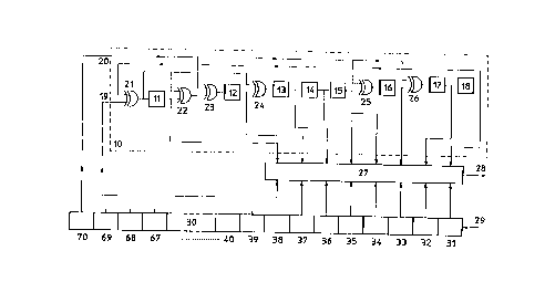
Figure 1 shows a device according to the invention, comprising
converting means according to the invention.
The device according to the invention, depicted in Figure l,
comprises converting means 10, comparing means 27 and a shift register 30.
Converting means 10 are equipped with an input 19 and a further input 20,
with eight memory elements 1 l, 12, 13, 14, 1 S, 16, 17 and 18, and with six
combining devices 21, 22, 23, 24, 25 and 26.
Converting means 10 thus comprise a first combining device 21 of
which a first input is coupled to an input 19 of converting means 10 and of
which a second input is coupled to an output of an eighth memory
element 18, of which eighth memory element 18 an input is coupled to an
w0 95/18495 PCT/EP94/04272 - -
2 ~ 79296
to
output of a seventh memory element 17, of which seventh memory
element 17 an input is coupled to an output of a sixth combining device 26,
of which a first input is coupled to an output of a sixth memory element 16
and of which a second input is coupled to further input 20 of converting
means 10, of which sixth memory element 16 an input is coupled to an outFut
of a fifth combining device 25, of which a first input is coupled to an output
of a fifth memory element 15 and of which a second input is coupled to
further input 20 of the converting means 10, of which fifth memory
element 15 an input is coupled to an output of a fourth memory element 14,
of which fourth memory element 14 an input is coupled to an output of a
third memory element 13, of which third memory element 13 an input is
coupled to an output of a fourth combining device 24, of which a first input
is
coupled to an output of a second memory element 12 and of which a second
input is coupled to an output of first combining device 21, of which second
memory element 12 an input is coupled to an output of a third combining
device 23, of which a first input is coupled to an output of a second
combining device 22 and of which a second input is coupled to further
input 20 of converting means 10, of which second combining device 22 a
first input is coupled to an output of a first memory element 11 and a second
input is coupled to the output of first combining device 21, of which first
memory element 11 an input is coupled to the output of first combining
device 21, the eight outputs of the memory elements 11 to 18 inclusive each
being coupled to one of the eight outputs of converting means 10.
These eight outputs of converting means 10 are each connected to one
of the eight one inputs of comparing means 27, which are further equipped
with an output 28. Shift register 30 comprises forty memory sections 31 to
70 inclusive, and an input 29. The eight outputs of memory sections 31 to 38
-. ,_. WO 95/18495 217 9 2 9 6 p~~4~~272
11
inclusive are each connected to one of the eight other inputs of comparing
means 27. The output of memory section 38 is coupled to input 19, and the
output of memory section 70 is coupled to further input 20 of converting
means 10.
The bit stream in which a boundary is to be established, is fed to
input 29 of shift register 30. Memory sections 31 to 38 inclusive contain the
third number of bits, in this case eight bits (one byte), which are fed to
comparing means 27. On the outputs of converting means 10 there appears
the second number of bits, in this case eight bits (one byte), which are
likewise fed to comparing means 27. As soon as the second number of bits
and the third number of bits agree with one another, comparing means 27
generate a synchronization signal via output 28. Memory sections 39 to 70
inclusive contain the first number of bits, in this case thirty-two bits (four
bytes) which are convened by converting means 10 to the second number of
bits. It should be noted in this context that converting means 10 do not
process the bits present on inputs 19 and 20 until after one clock pulse
period
(because of the presence of the memory elements), which affects the choice of
the bits to be fed to inputs 19 and 20. This is because during one earlier
clock pulse period the first number of bits is located in memory sections 38
to
69 inclusive, and the at least one bit situated outside the first number of
bits
(the thirty-third bit) is located in memory section 70.
This conversion process has hitherto been effected by calculating a
CRC (Cyclical Redundancy Code) over the first number of bits on the basis of
a generator polynomial associated with the CRC, for example G(x)=x8+x2+x+1
(or 100000111 ). The first number of bits, that is the first four bytes U(x),
are multiplied by x$ (or padded with 00000000 on the Least-Significant-Bit
side), after which a division is carried out by G(x), which yields a value
Q(x)
WO 95/18495 PCT/EP94104272
11929b 12
and a remainder R(x). The CRC over U(x) is then equal to the remainder
R(x). Said remainder R(x) corresponds to the second number of bits.
According to the invention, the conversion process is now effected by
only one bit of the first number of bits, namely the bit present in memory
section 38 (during one earlier clock pulse period), being fed to input 19 of
converting means 10 and by a bit situated outside the first number of bits,
namely the bit stored in memory section 70 (during one earlier clock pulse
period) being fed to input 20 of converting means 10. Partly as a result of
discounting means 23, 25 and 26 (three combining devices) being employed,
converting means 10 generate exactly the same result as converting means
known hitherto, which perform the complete CRC calculation mentioned
previously on the basis of the generator polynomial associated with the CRC.
It will obviously be necessary, if a different polynomial is used, for the
converting means in general and the discounting means in particular to be of
1 S different construction in order again to be able to generate the same
result as
convening means known hitherto, which perform the complete CRC
calculation mentioned previously on the basis of the other generator
polynomial.
The eight memory elements of converting means 10 form a feedback
series circuit of a fourth number of memory elements, which fourth number
in this case is therefore equal to eight. The six combining devices are
located
in this series circuit. This series circuit comprises combining device 21 for
coupling memory element 11 to input 19 of converting means 10 for
receiving at least one bit situated within the first number of bits, and to
memory element 18. This series circuit further comprises combining
devices 23, 25 and 26, respectively, for coupling memory elements 12, 16
and 17, respectively, to further input 20 of converting means 10 (for
WO 95/18495 PC"T/EP94/0427Z
2179296
13
receiving at least one bit situated outside the first number of bits) and to
memory elements 11, 15 and 16, respectively. The memory elements are
formed, for example, by flip-flop circuits, and the combining devices are
formed, for example, by modulo-two adders or EXOR gates.
The operation of convening means 10 will be explained in more
detail with reference to the following. Without the use of discounting
means 23, 25 and 26 and further input 20, converting means 10 generate the
CRC on the basis of the generator polynomial G(x)=x8+x2+x+1 (or
100000111 ) of precisely thirty-two bits U(x) shifted in, which otherwise are
multiplied to this end by x$ (or padded with 00000000 on the Least-
Significant-Bit side), after which a division is carried out by G(x), which
yields a value Q(x) and a remainder R(x), which remainder R(x) corresponds
to the CRC. All this is easily proved by mathematical induction in a manner
known to those skilled in the art. If then a subsequent bit is shifted in via
input 29 of shift register 30, there appears on the eight outputs of
converting
means 10 a CRC of not thirty-two but of thirty-three bits which is obviously
undesirable. The effect of the thirty-third bit (during one further clock
pulse
period present in memory section 70) therefore should be discounted. This is
done thanks to the use of discounting means 23, 25 and 26, specifically as
follows.
Because polynomial divisions are linear operations, the effect of the
thirty-third bit can be determined in a simple manner by determining its
canonical pattern. This is done by the thirty-third bit, padded with thirty-
two
zeros (that is 100000000000000000000000000000000) being multiplied by
x8 (that is, padding with eight zeros or 00000000 on the Least-Significant-Bit
side), after which it is divided by G(x) (that is, 100000111 ), which yields a
value Q(x) and a remainder R(x) (that is, 01100010). Said remainder R(x) is
WO 95/18495 PCT/EP94/04272 - --
2172°6 14
the canonical pattern which, after having been multiplied by the bit value of
the thirty-third bit (one or zero) should be deducted in the conversion
process.
Since in terms of modulo-two deduction corresponds to modulo-two addition,
the bit present in memory section 70 should therefore be fed, via three
modulo-two adders, 23, 25 and 26, respectively, to the second memory
element 12 (because of 01100010), the sixth memory element 16 (because of
01100010) and the seventh memory element 17 (because of 01100010),
respectively. Thus the effect of the thirty-third bit has thereby been
deducted during the conversion process, as a result of which the correct CRC
will after all appear on the eight outputs of converting means 10.
It should again be emphasized that if a different polynomial and/or
different first, second and/or third numbers of bits are used the construction
of the device shown in the figure will change. The invention is therefore not
restricted to the specific embodiment shown, but comprises both any devices
1 S for establishing boundaries which are provided with discounting means and
any converting means which belong to these devices and are provided with
discounting means.