Note: Descriptions are shown in the official language in which they were submitted.
~179995
WO95/20289 F~ 75~
A MET.HOD FOR OFF-HOOK DETECTION D~RTT\Tr- RTl~rGTl\TG AND T~TR USE OF
A SU13S(~RTRRR r,T~R INTRRT~'~rR CIRCUIT FOR OFF-HOOK DBT_CTION
DrJRING RINGT~G
.
5 TFrR~Ir~T~ FIRr~n OF T~E INVENTION
The present invention relates to a method for off-
hook detection during ringing in a subscriber line interf ace
circuit as well as the use of a subscriber line intPrfAce
circuit for above tinnP~l detection
DESCRIPTION O~ RRr,~Tr~n ART
InstAllAtinn costs for new copper lines are
increasing and make up a large part of the total installation
cost. The admass society of tomorrow will have a need for
15 higher capacity than what the copper/coaxial caole systems of
today can handle. New teleservices will be introduced, which
will deman~ ~igher information transfer together with the
expansion of the cable television networks. Through coordina-
tion of the teleservices with TV on the same optical f ibre
20 the inStAllAti~n c08ts could be lowered considerably. The
last bit to the subscriber is however still paired cable of
copper.
With short lines there does not e~ist a need for as
strong ringing signals out from the line as with long lines.
25 The lower voltages ~or ringing on the line interface board
enables ringing with an integrated circuit, the so called ~ -
subscriber line interface circuit (SLIC), which means that no
ring-trip relay is required. A problem which however needs to
be solved is to quickly trip the ringing signal when the
30 subscriber lifts the phone in order to prevent the strong
currents which otherwise threaten to destroy the SLIC.
At convPnti~n~l ring trip detection, i.e. the
detection of when the subscriber lif ts the phone during the
ringing process, the DC shift is ~lPtP~'tP~l, which occurs when
35 the phone is lifted (off-hook~ and thereby opens a DC path ln
the loop. It should however be pointed out that the bell is
AC coup l ed .
Wo 9S/20289 ~ ~ 7 9 ~ g ~ io I ~
There QXists within the art several diferent types
of devices and methods for the detection of this ~C shift.
See for instance Patent Abstracts o Japan, Vol 7, no. 200,
E-196, abstract of JP-A-58-979S0 (FUJITSU K K), June 10th
1983 och Patent Abstract8 oî Japan, Vol 7, no. 200, E-196,
abstract of JP-A-58-97949 (FUJITSU K.K), June 10th 1983 US-
A-4 132 864, DE-B2-2014950, US-A-4 455 456 1~11 of these
documents thus describe different ways of detecting the
occurence oi~ a DC level in the ringing signal.
The voltage range in a SLIC is however limited, why
it would be flP~i r~hl e to remoYe the DC level which normally
occurs when the hook is of f during ringing . A SLIC is
described in Swedish Patent Application ~o. 9400185-6, which
comprises a ringing signal generator and a loop which removes
the DC level from the ringing signal when the hook is off
during ringing.
Yet another device which detects the o~f-hook con-
dition during ringing is described in WO-Al-9301676 (FUJITSU
LIMITED et. al. ), 2 January 1993 . This device detects when a
ringing current through a resistor, which is connected in
series with a ring signal generator, exceeeds a thl~eshold,
which rlPtP~;on causes a detection signal for o~f-hook during
ringing to be emitted by the device. This ringing signal does
also include a DC component during off-hook. In this device
the time the thrQshold is P7~- Pe~Pd does not seem to be used
in the 1 nfli cpt; nn of o~-hook during ringing.
According to the specif ication P,~LLCORE TR-TSY-
000057 the ringing signal shall be disconnected from the
telephone within- 200 ms after a resistance o~ 300 Q is coup-
led to the li~e, which shall have a loop resistance ~ (Rdc -
400) Q, where Rdc = the line resistanoe + 430 Q, i. e. the
resistance in the p~irPfl ~-~hlP to the subscriber + 400 n
which shall represent an ordinary tPl p~h~nP + 30 Q which
represents the resistance ~rom the connection box.
The ring trip detector shall on the other hand not
react upon coupling o~ 10 kQ + 8 IlF or coupling of 200 Q
during 5 12 ms.
WO 95l20289 2 1 7 9 9 9 5 ~ 7.J,~
SllMMARY
The obj ect of the present invention is to provide of f -hook
indication during the occurence of a ringing signal, which
preferably lacks a DC r~ ~lnnf~nt, with certainty and in a fast
5 and simple way that can be accomplished with a SLIC that is
only slightly modified.
This object is achieved through a method with the
steps of
generating a signal which is a function of the0 line current through the subscriber line,
measuring the time the signal exceeds a first
reference value, which represents a predeto~minP~ current
value,
comparing the measured time with a predetermined
15 time value and
indicating off-hook in dependence of the
comparison .
Yet another object of the present invention is to
provide a method for the provision of off-hook indication
20 upon the occurence of a ringing signal without DC component
which is even faster than the first m~nti nn~rl method.
This obj ect is achieved through the signal being a
function of the absolute value of the line current.
Yet another object of the present invention is to
25 avoid unnecessary ostill~tinn in the off-hook indication.
This object is accomplished through the measuring
step including measuring of the time rom when the signal
rises above the first reference value to when it falls below
a second reference value, which is slightly offset from the
30 first reference value,
Yet another object of the present invention is to:
provide a new use of a SLIC.
This obj ect is achived through the use of a SLIC to
detect the of f -hook condition upon the occurence of a ringing
35 signal, whereby a detector which is included in the SLIC is
arranged to generate a signal which is a function o~ the line
current through the subscriber line and to measure the time
WO 95/20289 2 1 7 9 9 9 ~ c 1~, ~
the signal exceeds a fir6t reference value (Vth), which
represents a prP-lPtPrm; nPrl current value, and emit a 6ignal
representing the measured time to a processar for camparison
with a predetermined time value far the indicatian a~ a~f-
hook during ringing.
Other ob; ects and advantageL of the present inven-
tion will be made clear through the follawing descriptian and
claims .
BRIEF DESCRIPTIDN OF TE~E DRAWINGS
The present invention is described in more detail
below where re~erence is ~eing made to the appended drawings,
where -- :
fig. 1 shows a SLIC which performs the method
according to a first ' ~'; of the present invention,
fig. 2 shows a diagram of the line current as well
as the voltage over the line wires during on-hook and off-
hook,
fig 3 shows graphs of the line current during off-
hook and on-hook as well as the output of a detector which is
i n~ rl in the SLIC,
f ig . 4 shows a circuit which implements part of a
second method ~ i ng to the present invention and
f ig . 5 shows graphs of the line current during on-
i~i hook and off-hook as well a~ output signals from the detector
in a SLIC comprising the circuit in f ig . 4
DETAILED DESCRIPTION OF EMBODIMENTS
Accarding to the invention the current difference
is detected, which ap~ear because of the impedance difference
between the imrPr1~nr-P of the bell~s) and the i P~Prh~nP
1 ~PlPrhnnP, 1 REN: 7 kS2 relative to 7 kn//4oo n ~ 7 k
relative to 378, i e. an impedance difference o~ 18,5 times.
~ ~PlPrh~1nP~ 5REN: 1,4 kQ relative to 1,4 kn//400 n ~ 1,4 k
relative to 311, i e. an impedance di~erence of 4,5 times.
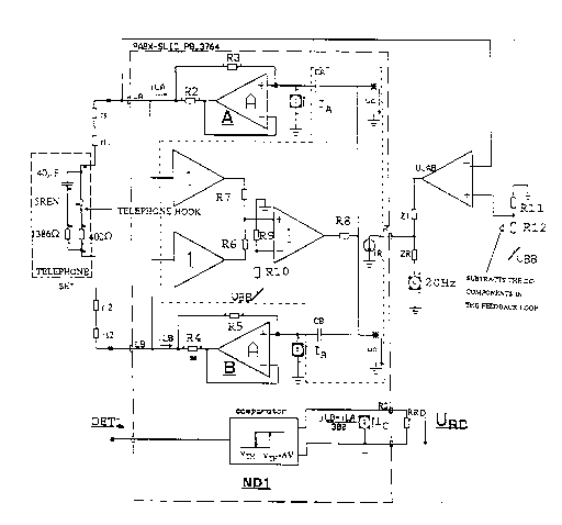
Fig 1 shows a subscriber line interface circuit
PABX-SLIC PB~3764 which according to a first embodiment of
~ WO 95/20289 2179 9 9 5 r ~ sl~ lOI
the method according to the invention detects of f -hook durng
ringing. In the figure a tPl PrhnnP 5 REN is shown as a resi6-
tance of 400 Q in series with a switch (TEI.EPHONE HOOK),
which are ~-nnnPc~PA in parallell with a re8istance of 386 Q
5 in series with a capacitor of 40 ~LF. A fir8t end of the tele-
phone 5REN is connected to one input LA on the S~IC via one
of the subscriber line wires, which wire includes the line
resistance rll and the protection resistance rsl. The input ----:
LA is connected to the output of a current amplifier A via a
0 measuring resistance R2, where the inverting input of the
ampl if ier A is connected to the output and the non- inverting
input i5 connected to the subscriber line via a resistance
R3 The non-inverting input of the current amplifier A is
also connected to a potential uc via a capacitor CA A
15 current source IA which is APrPn~Pnt of the potential uc is
also connected between the non-inverting input of the current
amplifier A and ground. A second end of the tPl PrhnnP 5REN is
in the same manner connected to an input LB on the SI,IC via
the other subscriber line wire, which includes the line
20 resistance rl2 and the protection reslstance rs2. The input
~B is connected to the output of a current amplifier _ via a
measuring resistance R4, where the inverting input of the
amplifier ~ is r--nnP~tPA to the output and the non-inverting
input is connected to the subscriber line via a reslstance
25 R5. The non-inverting input of the current amplifier _ is
also c~nnected to a potential uc via a capacitor CB. A
current source IB which is dependent of the potential uc is `~~
also connected between the non-inverting input of the current
amplifier B an~ ground. The inputs LA and LB of the SI,IC are
30 also, each via an amplifier w~th the amplification of 1 in
serie8 with a resistance R7 and R8, respectively, connected
to the non-~inverting input of an operational amp-li~ier with
amplification 1, whose inverting input is connected to the
interconnection point between two equally large resistances
35 R9, R1~ who are connected in 8eries, which resistances are
connected between ground and the supply voltage VBB of the
Wo 95/20289 217 9 9 9 ~ r~ o / ~
SLIC. The output o~ the latter operatiqnal ampli~ier i8 via
yet a resistance ~3 connected to the potential uc.
The above described components are of te~ u6ed in
SLICb and their functions are well known and will not be
5 further described in this description.
In f ig . 1 one of the subscriber line wires LA is
also rnnnPrtPfl to the first input of an opPrPtinn~ll amplifier
WAB, whose other input is connected to the interconnectiOn
point between two erually large resistances R11, R12 who are
10 connected in series, which resistances are connected between
ground and the supply voltage VBB oi~ the SLIC
The output of the r,rPr~tinn:~l amplifier WAB is
connected to the current input R of the SLIC via a resistance
ZT A 20 Hz signal ~nPr~tnr U is a~lso cornected to this
15 current input R via a resistance ZR. The current through the
current input R supplies current to the current amplifiers A
and _ in and for ~ t;nn of these to gen,erate the ringing
signal. This device provides ringing in the SLIC without any
DC component and is discribed in more detail in Swedish
i~ patent application 9400185-6
In ~ig. ~ is finally shown a detector ~1, which
originally was arranged for~o+~-hook detection although not
during ringing. The det,ector ~ inrl~ P~ a comparator. A
dependent current source ID is connected across the input of
25 the ~ comparator, which also serves as an output RD of the
SLIC. Across this output RD is a resistance RRD connected.
The output DETl of the comparator is connected to a processor
(not shown) which is P7rtPrn~l to the SLIC. This processor is
also arranged to bP able to triF the ringin, current from the
30 ring signal generator ~J. The dependent current source ID in
the detector ~1 is in a known way rnnnPctprl to the measuring
resistances R2 and R4 (not shown) in order to generate a
current which is a linear function of the line current.
Fig. 2 shows a simulation o~ the line current il
35 during ringing, where il = iLB -iLA, and with a load of 5REN
~bell = ~00 n + 2 I~F + 22 H) and a line resistance of 0 Q and
the fres~uency 20 Hz as a i~unction o~ time at on-hook and off-
W095/20289 ~,~, 7ggg5 r~ 0,
hook states. In the ~igure is also shown a simulation of the
voltage at the A-wire (TIP) which represents LA as well as
the voltage at the B-wire B (RING) which represents LB. In
the figure one can see that the voltage up to the time
indicated by the dashed vertical line is phase displaced from ''
the current approximately -60, at which point in time the
of f -hook state occurs and the current rapidly rises and
current and voltage are substantially in phase. Although it
is not clearly shown here the line current il does not
0 include any DC-~ n~ in the off-hook state as it is the =:
r- ~ry value of the line current il,
Fig. 3 shows measured results from a device accor~
ding to fig. l for off-hook detection during ringing. In the
figure~ the line currents il (lREN) and il ~5REN) are shown
together with the output signal ~ from the detector NDl,
Referring to fig 1 and 3 the method according to the ~irst
embodiment of the invention is carried out in the following
manner: ' ' =
The current that leaves the current amplif ier A ~~
20 (-iLA) and the current that goes into the current amplifier R
(=iLB) are measured in the ~ ringen resistances R2 and R4
and are summed (iLB-iLA) in order to obtain the transversal
line current in the dependent current source ID of the
detector NDl. A voltage ~unction r~RD of the transversal line ~'
25 current (iLB-iLA) /300, which is determined through the
resistance B~D and the ~PrPn~nt current source ID, is then
coupled into the detector D1. The detector levels Vth and
Vth-~V are through choice of the resistance RD set for the
detection of the time ~t from when the line current il rises
30 above a first predetermined current value to when it falls
below a second prede~Prm;nP~ reference value. The second pre- ~ ~
detPrminP-9 referencè value is slightly of~set from the first
reference value, preferably with 1 - 2~ of the first refe-
rence value, and both are set in an interval between the
35 maximum on-hook line current and the maximum off-hook line
current. The output ~1 Of the detector NDl has a high
signal level as long as the line current il is lower than the
W09sl20289 ,. ~ Ol
21~9~9~ 8
predetermined current levels. When however the line current
il rises above the first prP~Ptprm;np~l current level the
output D~T1 yoes low and stays low until the line current il
falls below the second prP~lPtPrml netl current leYel . The
5 second level is o_fset from the ~irst i~ order to achive
hysteresis The output DETl of the detector ND1 is then
processed in the processor in order to indicate the off-hool~
state in such a way that the time ~t that the output ~;L
stays low is compared with a predetermined time lenght,
10 preferably a sixth of the period of the ringing signal, and
of ~-hook is ;n~l;r~3tPfl if this predetPrm;nP~ time length is
P~rrPP.lP~, af ter which the processor trips the ringing .
This method shows the following advantages:
1) No extra detector for detecting off-hook during
15 ringing is needed, which means that less chip area ls needed.
2) No PYtl~rn~l ring trip network is needed, which
means f ewer external components ~
The difference in line current between on-hook and
off-hook ringing i8 not r~uite proportional to the line load,
2C due to the ~act that the amplification 4 ~ 2 is not constant.
A current difference of about 2, 7 times is obtained
in the worst case, which di~ference should be possible to
detect with a current sensing loop detector.
In fig. 4 is shown a circuit which 1r~rl~ ' ¢ a
25 dependent current source in a SLIC which performs a method
Arrnrrlinrj to a gecor,d Pmhn~; t of the present invention.
This circuit already exists in the SLIC named PALX-SLIC
PBL3799 and comE)rises four voltage/current ~T~l i f;~r~¢ 1, 2, 3
and 4, whereby the voltage/current amplifiers l, 2 are
3~ rnnnPrtprl acrogs the resigtance R2, which in fig. 1 is
rnnnPrte~, to the input LA and the amplifierg l, 2 each supply
a current IA/E and -IA/~{' which both represent the current IA
and K is a constant. The voltage/current amplifiers 3, 4 are
in the same way connected across the resistance R4, which in
fig. 1 is rnnnPrtPrl to the input LB, and which amplifiers 3, --
4 each supply a current IB/E and -IB/E, which represent the
current IB and E is a c~nstant. The outputs of the vol-
~j WO95/20289 2~7999~ r~ .O,
tage/current amplifiers 1, 3 are interconnected ana connected
to a first input terminal of a comparator via a first diode
Dl. The outputs of the voltage/current amplifiers 2, 4 are
in the 8ame manner interconnected and connected to the same
5 input terminal of the comparator via a second diode D2. The
second input terminal of the comparator is grounded and the
resistance RRD is connected between these two tP~m; n;:ll s . In
this figure the two current amplifiers A and B from fig. 1
are also shown. The currents IA and IB represent -iLA and iLB
from fig. 1. The voltage/current amplifiers 1, 2, 3 and 4
together with the diodes D1 and D2 in this CilCUit together
make up a dependent current source which emit a current ID
that is a function of the absolute value of the line current.
This current ID runs through the resistance RRD and the
1~ voltage thereacross ID*RRD is used as a signal representing
the absolute value of the line current and is supplied to the
comparator. On the output of the comparator a output signal
DET2 is then obtained. If the amplifiers 2 and 4 as well as
the diodes D1 and D2 are removed the dPpPnAPnt current source
20 according to fig. 1 is obtained.
In fig. ~ is finally shown simulations of the line
current il with a bell of 5RBN and line resistance of 0 Q and
a bell of lREN and line resistance of 200 Q, both with a
frequency of 20 Hz, and the output signal from the detector
25 ~=~rrnr~;ng to fig. 4 for these signals at on-hook and off-
hook states. The telephone hook is on up to the time
indicated by the solid vertical line designated Off-Hook, at
which point in time the off-hook state occurs and the line
current il increases. The output DET2 of the detector ND2 has
30 a low level up to the above mPntinnPfl point in time but when
the absolute value of respective line current rises above the
f irst predetermined current value the output DET2 of the
detector goes high and stays high until the~ line current il
falls below the second predetPrm;nPrl current level The time
35 ~t that the output DET1 stays low is then transmitted to the
processor in the form of a pulse. In the figure two pulses ~t
are shown in order to illustrate taht the detector ND2 reacts
wo 95120289 2 1 7 9 g 9 5 L ~ ~ 0 iO ~ ~
upon both the positive and negative half periods o~ the line
current, but in reality the ring signal generator is switched
off after the first pulse. In the case of lR13N a pulse width
~t of 17 ms was obtained and in the case of 5REN a pulse
width Qt of 21 ms. The predetermined time value they are com-
pared with is pre~erably a sixth of the ringing period, i e.
about 8, 3 ms . When this time value is P~CPP~qP~ the processor
in~l; rAt~c oEf-hook and therea~ter trips the ringing signal .
The advantage of this second method is that off-
10 hook detection during rirging is ;3rrnmrl; ch~-9 during both the
half periods of the line current il, which makes this method
faster than the first method.
A nu~mber of simulations (not shown) have also been
made f or this second e~odiment of the method at dif f erent
ringing loads, line resistances as well as telephone
resistances than what is I tinnPfl in TR-TSY-0~0057. They all
show that acceptable pulse widths are obtained that exceed
the, t;nnPrl prPcl~tPrm;n~-l time value
If it is desired that the original use of the
20 detector ~ according to fig. 1 for the off-hook detection
without ringing should be retained whilst performing a method
according to the invention one can easily devise a new detec-
tor for the off-hQok detection during ringing. This can
either be nrr~ ~1; ch~rl through the inclusion o~ a new detec-
tor with its own dependent current source, i.e. a doubling of
detectors or through connection o~ an external ~Ptertnr to
the output RD of the SLIC, in- which latter case the existing
rlPrPn~nt current source in the detector in the SLIC is used
f or both the det~ctors .