Language selection

Search

Patent 2180100 Summary

Third-party information liability

Some of the information on this Web page has been provided by external sources. The Government of Canada is not responsible for the accuracy, reliability or currency of the information supplied by external sources. Users wishing to rely upon this information should consult directly with the source of the information. Content provided by external sources is not subject to official languages, privacy and accessibility requirements.

Claims and Abstract availability

Any discrepancies in the text and image of the Claims and Abstract are due to differing posting times. Text of the Claims and Abstract are posted:

  • At the time the application is open to public inspection;
  • At the time of issue of the patent (grant).
(12) Patent: (11) CA 2180100
(54) English Title: HIGHER ORDER DIGITAL PHASE LOOP FILTER
(54) French Title: FILTRE A BOUCLES DE PHASE NUMERIQUE D'ORDRE SUPERIEUR
Status: Expired and beyond the Period of Reversal
Bibliographic Data
(51) International Patent Classification (IPC):
  • H03H 17/02 (2006.01)
  • H03L 07/10 (2006.01)
  • H04L 27/06 (2006.01)
(72) Inventors :
  • BHATT, BHAVESH BHALCHANDRA (United States of America)
(73) Owners :
  • RCA THOMSON LICENSING CORPORATION
(71) Applicants :
  • RCA THOMSON LICENSING CORPORATION (United States of America)
(74) Agent: CRAIG WILSON AND COMPANY
(74) Associate agent:
(45) Issued: 2006-04-11
(86) PCT Filing Date: 1994-01-12
(87) Open to Public Inspection: 1995-07-20
Examination requested: 2000-12-21
Availability of licence: N/A
Dedicated to the Public: N/A
(25) Language of filing: English

Patent Cooperation Treaty (PCT): Yes
(86) PCT Filing Number: PCT/US1994/000390
(87) International Publication Number: US1994000390
(85) National Entry: 1996-06-27

(30) Application Priority Data: None

Abstracts

English Abstract


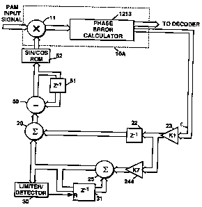
A higher order phase loop filter includes an integrator consisting of an adder (25) and a delay element (31) arranged in a feedback
loop between the output port of such adder and one of its input ports. Signal to be filtered is applied to a second input port of the adder.
A detector (30) is coupled to the output of the adder to detect limiting values, which, when detected, conditions the detector to reset the
current value in the delay element of the integrator to a fixed value such as zero. Resetting the delay element momentarily lowers the order
of the filter and speeds system response time in the presence of noise.


French Abstract

Un filtre à boucles de phase d'un ordre supérieur comprend un intégrateur consistant en un additionneur (25) et un élément retard (31) agencé dans une boucle de réaction entre le port de sortie de l'additionneur et l'un de ses ports d'entrée. Le signal à filtrer est appliqué à un second port d'entrée de l'additionneur. Un détecteur (30) est couplé à la sortie de l'additionneur pour détecter des valeurs limites qui, lorsqu'elles sont détectées, conditionnent le détecteur afin que ce dernier rétablisse la valeur actuelle dans l'élément retard de l'intégrateur à une valeur fixe telle que zéro. Le rétablissement de l'élément retard abaisse momentanément l'ordre du filtre et accélère le temps de réponse du système en présence de bruit.

Claims

Note: Claims are shown in the official language in which they were submitted.


7
CLAIMS
1. In a carrier recovery circuit including a loop filter (14) of
the form which includes a signal summing circuit (25) and a signal
storage element (31) coupled between an output port and an
input port of said signal summing circuit to form an integrator, an
improvement comprising; detection means (30) coupled to said
signal summing circuit, for detecting when sums output from said
signal summing circuit exceed predetermined limits, and for
resetting signal in said storage element to a predetermined value
when such sums exceed such limits.
2. The circuit set forth in claim 1 wherein said means
responsive to the detection of sums exceeding such limits, resets
signal in said storage element to a zero value.
3. A loop filter for a phase locked loop comprising:
a source of error signal (10);
a adder (20) having first and second input terminals, and an
output terminal for providing filtered error signal;
a first circuit path (22, 23) coupled between said first input
terminal and said source, and including a series connection of a
first signal scaling circuit and a delay element;
a second circuit path (24, 25, 31) coupled between said
second input terminal and said source, and including a signal
integrator, said integrator including:
a signal summing circuit (25) having a further signal
delay element coupled between an output port and an input port
thereof;
a detector (30) for detecting when sums provided by
said signal summing circuit exceed predetermined values, and for
resetting said further delay element (31) to a predetermined
value when said sums exceed such predetermined values.
4. The loop filter set forth in claim 3 wherein said detector
resets said further delay element to a zero value.

8
5. Apparatus including a loop filter comprising:
a source of signal including a carrier component;
a multiplier having a first input coupled to said source,
having a second input and an output terminal;
phase calculating means, coupled to the output terminal of
said multiplier, for providing at an output terminal thereof, a
phase error signal indicating the difference in phase of said
carrier component from a desired carrier phase;
an adder having first and second input terminals, and an
output terminal for providing filtered error signal;
a first circuit path coupled between said first input terminal
of said adder and said output terminal of said phase calculating
means, and including a series connection of a first signal scaling
circuit and a delay element ;
a second circuit path coupled between said second input
terminal of said adder and said output terminal of said phase
calculating means, and including a series connection of a second
signal scaling circuit and a signal integrator, said integrator
including:
a signal summing circuit having a further signal delay
element coupled between an output port and an input port
thereof;
a detector for detecting when sums provided by said
signal summing circuit exceed predetermined values, and for
resetting said further delay element to a predetermined value
when said sums exceed such predetermined values.
means including a differentiator coupled between the output
terminal of said adder and the second input terminal of said
multiplier.

Description

Note: Descriptions are shown in the official language in which they were submitted.


WO 95/19676 PCT/US94/00390
1
HIGHER ORDER DIGITAL PHASE LOOF FILTER
This invention relates to circuitry for recovering pulse
amplitude modulated, PAM, signals, and more particularly to loop
filters utilized in such systems.
BACKGROUND OF THE I1V'VFNTION
PAM signals occur in several forms such as Quadrature
Amplitude Modulated (QAM), Phase Shift Keying (PSK), and
Quadrature Phase Shift Keying (QPSK), for example, the
information of which are characterized by constellations
representing a fixed number of discrete amplitude values.
Recovery of the transmitted information requires recovery of the
signal modulation carrier with appropriate phase control to insure
proper orientation of the constellation. Typical PAM signal
1 S recovery systems are described ty Lee and Messerschmitt in
chapter 14 of DIGI i AL COMMUNICATION, Kluwer Academic Pub.,
Boston Ma., 1992, an example of which is illustrated in Figure 1
herein.
The FIGURE 1 apparatus includes a source of PAM signal
2 0 (not shown) which is applied to a mixer 11. Mixer 11 may be a
complex multiplier, having a first input port for receiving the
PAM signal and a second input port for applying a recovered
carrier signal. The mixer 11 provides a baseband signal to a
phase circuit including a slicer 12 and a decision circuit 13. The
2 5 decision circuit 13 determines the difference between the
amplitude of the received signal and the amplitude of the most
probable constellation value, and outputs this difference as an
error e. The combination of the elements 11, 12 and 13 form one
of many alternative phase detectors (10). The outpput of the phase
3 0 detector is applied to a loop filter 14, which is incorporated to
provide a measure of noise immunity and to establish the system
timing capture parameters. The output t~f the loop filter is a
control signal, C, which is coupled to control a controlled oscillator
15. If the mixer 11 is realized in analog form the oscillator 15
3 5 may be an analog voltage controlled oscillator arranged to provide
two signals having a 90 degree phase relation. Alternatively, if

WO 95119676 PCT/US94/00390
2180100
2
the mixer is realized in digital form (i.e., to process digital PAM
signal) the oscillator may be a controlled discrete time oscillator
DrhO.
FIGURE 2 illustrates a known second order loop filter circuit
which, may be implemented for the filter 14 in FIGURE 1. This
fiter is shown realized with digital circuit ' elements and presumed
to operate in sampled data manner. In FIGURE 2, the error signal
a from the phase detector is applied to first and second scaling
circuits 23 and 24 which respectively weight the error signal by
1 0 weighting factors K1 and K2. Error signal samples which are
weighted in element 23 are delayed one sample period in delay
element 22 and applied to an adder 20. Error signal samples
which are scaled in element 24 are applied to an integrator
including a signal summing circuit or adder 25 and a one sample
1 5 period delay element 26 coupled between the output port of the
adder 25 and one of its input ports. The output signal from the
integrator is applied to a second input port of the adder 20 via a
limiter circuit 27.
It will be recognized by those skilled in filter design that the
2 0 upper circuit path provides a response to instantaneous signal
changes while the lower circuit path provides a response to longer
term signal trends. In the steady state the phase error is zero or
very small, and the transfer function H(z) of the FIGURE 2 circuit
may be represented by the equation;
25 H(z) = K1(z-1) + K2/(1-z-1). (1)
where K1 and K2 are constant weighting factors. Equation (1)
assumes that the output of the integrator is sufficiently small that
no signal limiting is incurred. However, if there is significant
noise in the received signal, the noise will be reflected in the error
3 0 signal, and the output of the integrator may be limited. Assume
that the limiting value is K3. When limiting occurs the transfer
function of the loop filter becomes;
H(z) = K1(z-1) + K3 (2)
The limiting action reduces undesirable effects due to signal noise,
3 S such as false lock. However, when the system is operating in the

__ WO 95/19676 PCT/US94/00390
21~01G0
3
limiting mode, the term K3 will normally dominate which results
in undesirably slow response times.
The present invention is intended to incorporate the
advantageous aspects of incorporating the effects of a limiter in a
S loop filter without incurring the undesirable aspects.
SUMMARY OF THE INVENTION
The present invention is a higher order phase loop filter
which includes an integrator of the form comprised of a siganl
summing circuit or adder and a delay element arranged in a
1 0 feedback loop between the output of such adder and an input
port. Signal to be filtered is applied to a second input port of the
adder. A detector is coupled to the output of the adder to detect
limiting values, which when detected, conditions the detector to
reset the current value in the delay element of the integrator to a
15 fixed value such as zero. Resetting the delay element
momentarily lowers the order of the filter and speeds system
response time in the presence of noise.
BRIEF DESCRIPTION OF THE DRAWINGS
The invention will be more readily understood with
2 0 reference to the drawings wherein;
FIGURE 1 is a block diagram of a prior art phase locking
system;
FIGURE 2 is a block diagram of a known loop filter of the
type which may be implemented for the loop filter 14 of FIGURE
25 1;
FIGURES 3 and 5 are block diagrams of loop filters
embodying the present invention; and
FIGURE 4 is a block diagram of a carrier recovery phase
correction system embodying the present inventiop.
3 0 DETAILED DESCRIPTTON
Refer to FIGURE 3 which illustrates an exemplary
embodiment of the invention. In the FIGURE an error signal e,
from for example, the phase detector 10 of FIGURE 1, is applied to
first and second scaling circuits 23 and 24 which respectively
3 5 scale the error signal by values K1 and K2. Exemplary values of
K1 and K2 are 1/4 and 1/32. Signal weighted by the factor 1/4

z~~o~oo PcT~us 940039 0
51 Recd PC~'~'~'TG 15 N 0 v 1995
from the scaling circuit 23 is coupled to a delay element 22. The
error signal is assumed to be a sampled data signal and the delay
element 22 delays signal by one sample period. Delayed signal
from delay element 22 is coupled to a first input port of an adder
20.
Signal weighted by the scale factor K2, from scaling circuit
24 is applied to an integrating circuit including a signal summing
circuit or adder 25 and a delay or signal storage element 31. The
delay element 31, delays signal sums output from the adder 25 by
one sample period, and applies the delayed sums to an input port
of the adder 25. The output sums from the adder 25 are coupled
to a second input port of the adder 20. The output sums from the
adder 25 are also applied to a detector 30, which provides a reset
signal whenever the sums provided by the adder 25 exceed
predetermined limiting values. (For a 16 bit adder the limiting
values may be ~4000 hexadecimal.) The reset signal provided by
the detector 30 is coupled to reset the value in the delay element
31 to a predetermined reset value such as zero.
For small valued error signals the transfer function of the
2 0 FIGURE 3 loop filter is described by equation 1. When signal noise
causes the integrator to generate output values in excess of the
limiting values, the transfer function is given by;
H(z) = K1 (z-1 ) + K2 ( 3 )
Note however, that the factor K1 is significantly larger than the
2 5 factor K2, thus the loop filter effectively, momentarily reverts to a
first order loop. That is the second term on the right side of
equation (3) may be ignored. When the loop filter reverts to a
first order loop it will inherently have a faster lock-in time, in the
presence of noise. In addition resetting the integrator to a small
3 0 value diminishes cumulative effects due to the signal noise.
In FIGURE 3, the detector 30 is illustrated as a limiter and
may in fact he realized with appropriate parts of limner circuitry.
However detector 30 may better be characterized as a window
comparator which provides an output signal having a first state,
3 5 e.g., zero, for all applied input values occurring between
AMENDED SHEET

WO 95/19676 PCT/US94/00390
2180100
designated limits, and a second output state, e.g., a logic one state,
otherwise.
The FIGURE 1 system is of the type which will correct both
frequency and phase errors. FIGURE 4 illustrates a system for
5 correcting only phase errors. In FIGURE 4 elements designated
with like numbers to elements in FIGURES 1-3 are similar and
perform similar functions. The phase detector l0A may be
similar to phase detector 10 of FIGURE 1 or it may take the form
of any other known phase detector. Phase corrected signal is
1 0 available at the output of the mixer 11. The loop filter is similar
to the loop filter shown in FIGURE 3, with the exception that the
second scaling circuit 244 is in cascade connection with the first
scaling circuit 23 rather than being in parallel as shown in
FIGURES 2 and 3. The weighting factor K7 of the second scaling
circuit 244 is arranged such that K1 times K7 equals K2.
Consider a QAM signal applied to the input of the mixer 11
and assume that the mixer 11 is a complex multiplier. The QAM
signal has in-phase I and quadrature-phase Q components.
Corrected component signals Ic and Qc may be obtained according
2 0 to the relationships given by;
Ic = I cos(9) + Q sin(8) (4)
Qc = Q cos(9) - I sin(8). (5)
If complex multiplier values representing cos(9) and sin(9) are
applied to the mixer from the loop filter, the complex multiplier
2 5 11 will inherently generate the phase corrected component
signals. The values cos(6 ) and sin(8 ) are quadrature
representations of the filtered error signal E.
Signal from the loop filter, that is from adder 20, are
coupled to one input port of a subtracter 50. The putput of the
3 0 subtractor is coupled to its other input port via a one sample
period delay element 51. The combination of subtracter 50 and
delay element 51 form a differentiator, which is in effect a
bandpass filter, that can only pass phase error changes. The
bandpass filtered (differentiated) phase errors are coupled to a
3 5 look-up table 52 which may be realized with a read-only-memory

WO 95/19676 PCT/US94/00390
z~ ~o~ 00
6
or ROM. The ROM provides pairs of values corresponding to cos(6)
and sin(6) values, where 8 is given by;
9 = (1/(1+z -1)}{K1(z-1) + K2/(1-z-1)}{e} (6)
FIGURE S is an example of a higher order loop filter using
the same limiting concepts as those illustrated and described with
respect to FIGURES 3 and 4. The dashed arrow between the
limiter/detector 301 and the delay element 312 is intended to
indicate that this connection is optional.

Representative Drawing
A single figure which represents the drawing illustrating the invention.
Administrative Status

2024-08-01:As part of the Next Generation Patents (NGP) transition, the Canadian Patents Database (CPD) now contains a more detailed Event History, which replicates the Event Log of our new back-office solution.

Please note that "Inactive:" events refers to events no longer in use in our new back-office solution.

For a clearer understanding of the status of the application/patent presented on this page, the site Disclaimer , as well as the definitions for Patent , Event History , Maintenance Fee  and Payment History  should be consulted.

Event History

Description Date
Time Limit for Reversal Expired 2010-01-12
Letter Sent 2009-01-12
Grant by Issuance 2006-04-11
Inactive: Cover page published 2006-04-10
Inactive: Final fee received 2006-01-27
Pre-grant 2006-01-27
Notice of Allowance is Issued 2005-08-18
Letter Sent 2005-08-18
Notice of Allowance is Issued 2005-08-18
Inactive: IPC assigned 2005-08-02
Inactive: First IPC assigned 2005-08-02
Inactive: Approved for allowance (AFA) 2005-06-09
Letter Sent 2005-02-07
Reinstatement Requirements Deemed Compliant for All Abandonment Reasons 2005-01-27
Amendment Received - Voluntary Amendment 2005-01-27
Reinstatement Request Received 2005-01-27
Inactive: Abandoned - No reply to s.30(2) Rules requisition 2004-02-26
Inactive: S.30(2) Rules - Examiner requisition 2003-08-26
Inactive: Status info is complete as of Log entry date 2001-02-06
Letter Sent 2001-02-06
Inactive: Application prosecuted on TS as of Log entry date 2001-02-06
All Requirements for Examination Determined Compliant 2000-12-21
Request for Examination Requirements Determined Compliant 2000-12-21
Amendment Received - Voluntary Amendment 2000-12-21
Application Published (Open to Public Inspection) 1995-07-20

Abandonment History

Abandonment Date Reason Reinstatement Date
2005-01-27

Maintenance Fee

The last payment was received on 2005-12-20

Note : If the full payment has not been received on or before the date indicated, a further fee may be required which may be one of the following

  • the reinstatement fee;
  • the late payment fee; or
  • additional fee to reverse deemed expiry.

Patent fees are adjusted on the 1st of January every year. The amounts above are the current amounts if received by December 31 of the current year.
Please refer to the CIPO Patent Fees web page to see all current fee amounts.

Fee History

Fee Type Anniversary Year Due Date Paid Date
MF (application, 4th anniv.) - standard 04 1998-01-20 1997-12-11
MF (application, 5th anniv.) - standard 05 1999-01-12 1998-12-23
MF (application, 6th anniv.) - standard 06 2000-01-12 1999-11-25
MF (application, 7th anniv.) - standard 07 2001-01-12 2000-12-21
Request for examination - standard 2000-12-21
MF (application, 8th anniv.) - standard 08 2002-01-14 2001-12-20
MF (application, 9th anniv.) - standard 09 2003-01-13 2002-12-19
MF (application, 10th anniv.) - standard 10 2004-01-12 2003-12-23
MF (application, 11th anniv.) - standard 11 2005-01-12 2004-12-23
Reinstatement 2005-01-27
MF (application, 12th anniv.) - standard 12 2006-01-12 2005-12-20
Final fee - standard 2006-01-27
MF (patent, 13th anniv.) - standard 2007-01-12 2006-12-08
MF (patent, 14th anniv.) - standard 2008-01-14 2007-12-06
Owners on Record

Note: Records showing the ownership history in alphabetical order.

Current Owners on Record
RCA THOMSON LICENSING CORPORATION
Past Owners on Record
BHAVESH BHALCHANDRA BHATT
Past Owners that do not appear in the "Owners on Record" listing will appear in other documentation within the application.
Documents

To view selected files, please enter reCAPTCHA code :


To view images, click a link in the Document Description column. To download the documents, select one or more checkboxes in the first column and then click the "Download Selected in PDF format (Zip Archive)" or the "Download Selected as Single PDF" button.

List of published and non-published patent-specific documents on the CPD .

If you have any difficulty accessing content, you can call the Client Service Centre at 1-866-997-1936 or send them an e-mail at CIPO Client Service Centre.


Document
Description 
Date
(yyyy-mm-dd) 
Number of pages   Size of Image (KB) 
Representative drawing 1997-06-24 1 7
Representative drawing 2003-04-24 1 8
Description 2001-02-20 6 280
Claims 2001-02-20 2 88
Abstract 1995-07-19 1 46
Description 1995-07-19 6 267
Claims 1995-07-19 2 83
Drawings 1995-07-19 2 41
Drawings 2006-04-09 2 41
Abstract 2006-04-09 1 46
Reminder - Request for Examination 2000-09-12 1 116
Acknowledgement of Request for Examination 2001-02-05 1 179
Courtesy - Abandonment Letter (R30(2)) 2004-05-05 1 167
Notice of Reinstatement 2005-02-06 1 170
Commissioner's Notice - Application Found Allowable 2005-08-17 1 161
Maintenance Fee Notice 2009-02-22 1 171
PCT 1996-06-26 10 387
Correspondence 2006-01-26 1 27
Fees 1996-12-18 1 60
Fees 1996-06-26 1 63