Note: Descriptions are shown in the official language in which they were submitted.
CA 02180387 2006-11-21
METHOD AND ARRANGEMENT FOR OPERATING ELECTRIC LAMPS
IN RESPONSE TO ANOMALOUS STATES
The invention relates to a circuit arrangement for operating electric lamps
and to an operating method for electric lamps.
Such a circuit arrangement is disclosed, for example, in the patent
specification EP-B 0 276 46. It serves the purpose of operating a low-pressure
discharge lamp and has an inverter which comprises two alternately switching
transistors arranged in a half-bridge. This circuit arrangement has a safety
shutdown which shuts down the inverter in the ease of anomalous operation. The
switch-off device essentially comprises a thyristor which is connected in
parallel
with the control electrode of a switching transistor of the inverter, and a
Zener
diode which controls the gate of the thyristor. In the case of an anomalous
operating state, the thyristor switches through and extracts the control
signal from a
switching transistor of the inverter and thus effects a shutdown of the
circuit
arrangement. The implementation of this safety shutdown requires a surge-proof
thyristor and a plurality of ohmic resistors of relatively high volume and
with a
loadability of a few watts, which serve the purpose of current limitation in
the
switch-off case and of generating the thyristor holding current. Moreover, it
is
necessary to use very robust transistors for the half-bridge, only in order to
withstand the load during the switching-off operation.
Offenlegungsschrift DE 43 34 076 likewise
2180387
= 2 -
describes a circuit arrangement corresponding to the
preamble of Patent Claim 1. it comprises a current
feedback half-bridge inverter which is equipped with a
switch-off device which switches off the inverter in the
case of a defective lamp by extracting the control signal
from a transistor of the inverter. The switch-off device
contains as essential elements a field-effect transistor,
which is connected in parallel with the control electrode
of the transistor, a bistable multivibrator which drives
the gate of the field-effect transistor, and a trigger
via which the bistable multivibrator is reset in the case
of a defective lamp, which has the effect of switching
through the field-effect transistor and thus of switching
off the inverter. A disadvantage of this circuit arrange-
ment consists in that as a consequence of the free-
wheeling diode which is necessarily present in the field-
effect transistor for technical reasons, the switch-off
device causes an asymmetric drive of the inverter
transistors. Moreover, particularly in the case of high
operating temperatures of the inverter transistors there
is the risk that the voltage present at the control
junction of the inverter transistor to be switched off
exceeds the base-emitter threshold vollpage of said
transistor during the switching-off operation, with the
result that this inverter transistor is not reliably
switched off, but instead operates in the linear range
and can be destroyed.
It is the object of the invention to provide a
circuit arrangement for operating electric lamps which
has a switch-off device which is improved by comparison
with the prior art mentioned above and which acts in the
case of an anomalous operating state and switches off the
inverter, and also to specify an improved operating
method for electric lamps.
This object is achieved according to the inven-
tion by means of the characterizing features of Patent
Claim 1 and Patent Claim 13, respectively. Particularly
advantageous embodiments of the invention are described
in the subulaims.
CA 02180387 2006-11-21
-~ -
The two circuit arrangements described above as prior art have a switch-off
device for the inverter which is based on the same fundamental principle. In
the
case of an anomalous operating state. the two switch-off devices extract the
control
signal from one of the half-bridge inverter transistors, by connecting a shunt
in
parallel with the control junction. The invention adopts a different approach.
In the circuit arrangement according to the invention, the switch-off device
for the inverter has a switch-off transistor whose switching junction is an
active
serial element of the control circuit of one of the inverter transistors, that
is, an
element across which the entire control current of this inverter transistor
flows in
normal operation of the inverter. The switch-off transistor is preferably a
field-
effect transistor which can be driven without power losses. The term control
circuit
is taken here to mean that circuit in which the control junction of the above-
mentioned inverter transistor is arranged. If this inverter transistor is a
bipolar
transistor, the control junction is the base-emitter junction of the inverter
transistor,
and the control circuit is the base-emitter circuit in which the control
current, that
is to say the base current, of the inverter transistor flows. If this inverter
transistor
is a field-effect transistor, the control junction is the gate-source junction
of the
inverter transistor and the control circuit is the gate-source circuit in
which the
control current, that is to say the gate current, of the inverter transistor
flows. The
entire control circuit of the relevant inverter transistor is switched between
a low-
resistance state - which corresponds to normal operation - and a high-
resistance
state - in the case of an anomalous operating state - with the aid of the
switch-off
transistor belonging to the switch-off device. In this case, the switching
junction of
the switch-off transistor of the switch-off device is arranged either in the
emitter
line or source line of the relevant inverter transistor (first exemplary
embodiment
of the invention) or else in the base line or gate line of the corresponding
inverter
transistor (second exemplary embodiment of the
4 -
invention). in the case of an anomalous operating state,
this arrangement according to the invention of the
switch-off transistor of the switch-off device ensures
for the inverter a reliable switching-off which still
functions acceptably even in the case of high operating
temperatures of the inverter, that is to say up to the
maximum permissible crystal temperature of the inverter
transistors and of the switch-off transistor.
During normal operation, the switching junction
- that is to say the drain-source junction - of the
switch-off transistor of the switch-off device, and thus
also the control circuit of the relevant inverter
transistor are of low resistance. After the occurrence of
an anomalous operating state, the switching junction of
the switch-off transistor, and thus also the control
circuit of the relevant inverter transistor are of high
resistance. This switchover into the high-resistance
state is preferably performed synchronously with the
blocking phase of the corresponding inverter transistor
with which the field-effect transistor is interconnected.
As a result, the switching transistors of the inverter
are reliably switched and only slightly loaded during the
switching-off operation, which is initiated by an error
signal monitoring element.
It is advantageous for the switch-off device
according to the invention to have a bistable switching
device whose input is driven by the error signal monitor-
ing element, via a trigger and/or time-delay switch, and
whose output is connected to the control electrode - that
is to say the gate electrode - of the switch-off
transistor, and which ensures by guidiag the supply
current via a lamp electrode that the inverter cannot
build up again until the exchange of the defective lamp
or until the circuit arrangement is switched on again. A
thyristor, or an equivalent thyristor circuit constructed
from two transistors, or a flip flop are advantageously
suitable as the bistable switching device. The above-
mentioned equivalent thyristor circult and the flip flop
have the advantage that they can be implemented using
CA 02180387 2006-11-21
-J -
integrated C-MOS technology.
The switching-off signal is advantageously formed by two components
superimposed on one another. The error signal monitoring element, which is
connected in parallel in terms of alternating current with the lamp or lamps
and
monitors the lamp voltage, generates a direct voltage which is proportional to
the
lamp voltage. This direct voltage forms the first component of the switching-
off
signal. It is advantageous further to superimpose on said direct voltage a
synchronization signal which is generated by a synchronization device which is
a
component of the error signal monitoring element and which forms the second'
component of the switching-off signal. This synchronization signal is
advantageously proportional to the temporal change in the voltage at the
centre tap
of the inverter switching transistors or to the time derivative of the
inverter output
voltage. As a result, the synchronization device ensures that the switching-
off
occurring in the case of a fault is performed during the blocking phase of
that
inverter transistor in the control circuit of which the switch-off transistor
of the
switch-off device is arranged.
The error signal monitoring element advantageously has a capacitor, a
rectifier diode and an RC integration element. The synchronization device
advanta-
geously contains a CR series circuit which is connected to the centre tap of
the
inverter and to the capacitor of the error signal monitoring element as well
as to the
input of the bistable switching device via a trigger and/or time-delay switch.
The invention is explained in more detail below with the aid of two
preferred exemplary embodiments.
Figure 1 shows a sketched circuit diagram of the circuit arrangement
according to the invention in accordance with the first
exemplary embodiment, and
Figure 2 shows a sketched circuit diagram of the circuit arrangement
according to the invention in accordance with the second exemplary
embodiment.
2180387
= = - 6 -
The two exemplary embodiments differ from one
another only in the arrangement of the switch-off
transistors T1, T1' of the switch-off device according to
the invention. For this reason, the same reference
symbols are used in Figures 1 and 2 for the identical
components of the two exemplary embodiments.
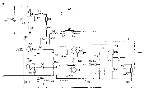
The circuit arrangement, illustrated in Figure 1,
in accordance with the first exemplary embodiment serves
the purpose of operating a 58 W fluorescent lamp LP. This
circuit arrangement has a half-bridge inverter fitted
with two bipolar transistors Q1, Q2. The two bipolar
transistors Q1, Q2 are each equipped with a freewheeling
diode Dl, D2, which are connected in parallel to the
collector-emitter junction of the appropriate transistor
Ql, Q2. In addition, the two bipolar transistors Ql, Q2
each have an emitter resistor R3, R4 and a base-emitter
parallel resistor R5, R6. Furthermore, an ohmic resistor
R7 and a capacitor C2 are connected in parallel with the
collector-emitter junction of the transistor Q1.
The two switching transistors Ql, Q2 of the half-bridge
are driven by means of a toroidal-core transformer which
has a primary winding RKa and two secondary windings RKb,
RICc. The primary winding RRa is integrated into the
series resonant circuit of the half-bridge inverter,
which is connected to the centre tap M of the inverter
and contains the coupling capacitor CR, the resonant
inductor LI and the resonant capacitor Cl. The secondary
windings RKb, RXc are each integrated into the base-
emitter circuit of an inverter transistor Ql, Q2 and
connected in each case via a base series resistor R1, R2
and an inductor L2, L3. to the base terminal of the
relevant bipolar transistor Q1, Q2. The half-bridge
inverter further has a starting device which essentially
comprises the diac DC and the starting capacitor C3. The
diac DC is connected via the inductor,L3 to the base
terminal of the inverter transistor Q2. The starting
capacitor C3 is connected to the negative pole of the
inverter direct voltage supply and, via an ohmic resistor
R10 and a rectifier diode D3, to the centre tap M of the
2180387
= - '1 -
half-bridge.
The fluorescent lamp LP to be operated is
connected in parallel to the resonant capacitor. One
connection of the first electrode filament El of the lamp
LP is connected to the resonant inductor Ifl, while the
other connection of the first electrode filament El is
connected to the resonant capacitor. One connection of
the second lamp electrode filament E2 is led to the
positive pole of the inverter direct voltage supply, and
the other connection of the second lamp electrode
filament is connected via an ohmic resistor RS to the
negative pole of the inverter direct voltage supply.
To this extent, the circuit arrangement
corresponds to a half-bridge inverter such as is
described, for example, on pages 62-63 of the book
"Schaltnetzteile" ["Switched-mode power supplies"} by
W. Hirschmann - A. Hauenstein, publisher Siemens AG.
After switch-on, the starting capacitor C3 is charged to
the breakdown voltage of the diac DC, which then
generates triggering pulses for the base of the bipolar
transistor Q2, and thereby causes the half-bridge
inverter to build up. After switching-through of the
transistor Q2, the starting capacitor C3 is charged via
the resistor RI0 and the diode D3 to such an extent that
the diac DC generates no further triggering pulses. The
two inverter transistors 91, Q2 switch alternately, with
the result that the centre tap,M of the half-bridge is
alternately connected to the positive or negative pole of
the direct voltage supply. The recharging of the coupling
capacitor CK occasioned thereby causes in the series
resonant circuit in the lamp -LP a medium-frequency
alternating current whqse frequency corresponds to the
operating frequency of the half-bridge inverter.
Connected in the emitter line of the second half-
bridge transistor Q2 is a field-effect transistor T1
which serves as switch-off transistor for the inverter
and is an essential component of the switch-off device
according to the invention. The drain of this field-
effect transistor TI is connected via the emitter
CA 02180387 2006-11-21
-8 -
resistor R4 to the emitter of the switching transistor Q2. The source terminal
of the
field-effect transistor T1 is connected to the negative pole of the direct
voltage
supply of the inverter. In normal operation, the drain-source junction of the
field-
effect transistor T1, and thus also the base-emitter circuit of the bipolar
transistor
Q2, are of low resistance. The base-emitter circuit of the bipolar transistor
Q2
contains the secondary winding RKc of the toroidal-core transformer, the base
series resistor R2, the inductor L3, the base-emitter junction of the bipolar
transistor Q2, the emitter resistor R4 and the drain-source junction of the
field-
effect transistor T1. Upon switching on the circuit arrangement, the field-
effect
transistor Tl is controlled in a low-resistance fashion before starting of the
inverter
via the closing resistor R11 and diode D4, which is led to the gate of the
field-
effect transistor T1. The gate of the field-effect transistor Tl is,
furthermore,
connected via a diode D5 to the output of a bistable switching device S whose
input is connected, for its part, to the output of an error monitoring element
[sic] F
connected parallel to the lamp LP in terms of alternating current. A Zener
diode D9
which limits the voltage drop to approximately 12 V is connected in parallel
with
the gate-source junction of the field effect transistor Tl. The aforesaid
bistable
switching device S and the error monitoring element [sic] F likewise belong to
the
switch-off device according to the invention, which in the case of an
anomalous
operating state controls the field-effect transistor TI and thus also the base-
emitter
circuit of the inverter transistor Q2 to be of high resistance. The
oscillation of the
half-bridge inverter is thereby interrupted. Switching off is performed
synchronously with the blocking phase of the switching transistor Q2. The
switch-
off signal is composed additively of two voltage components.
The first voltage component is a smoothed voltage which is proportional to
the lamp voltage. This voltage component is generated with the aid of the RC
integration
2180387
9 -
element R12, R13, C4, the rectifier diode D6 and the
capacitor CS. These aforementioned components R12, C4,
R13, C5, D6 are arranged in parallel in terms of alter-
nating current with the discharge path of the lamp LP.
One terminal of the capacitor C4 is connected to the
electrode filament El of the lamp, while its other
terminal is led via the resistors R12, R13 to the source
terminal of the field-effect transistor T1 and to the
negative pole of the inverter direct voltage supply. A
branch point located between the resistors R12, R13 is
connected via the rectifier diode D6 to a pole of the
capacitor C5. The other pole of the capacitor C5 is
connected to the negative pole of the inverter direct
voltage supply. The voltage divider R12, R13 divides the
voltage present at the lamp LP. This downwardly divided
voltage signal is fed to the capacitor C5 via the
rectifier diode D6 and integrated in the capacitor C5.
The capacitor C5 smoothes this voltage signal, with the
result that a direct voltage which is proportional to the
lamp voltage is present at the capacitor C5. This
smoothed direct voltage forms the first component of the
switching-off signal.
The second component of the switching-off signal
is a synchronization signal which is proportional to the
time derivative of the inverter output voltage at the
centre tap M and which is generated by a synchronization
device which is a component of the error monitoring
element [sic]. The synchronization devicg essentially
comprises a CR series circuit C6, R14, which forms a CR
differentiating element C6, R14. The capacitor C6 of the
differentiating element is directly connected to the
centre tap,M of the half-bridge, while the resistor R14
of the differentiating elemerit is directly connected to
a pole of the capacitor C5. The centre tap V of the
differentiating element C6, R14 is led via a lowpass
filter R15, C7, a rectifier diode D7 and a Zener diode D8
to the input of the bistable switchiag device.. The
differentiating element C6, R14 differentiates the
trapezoidal output voltage, present at the centre tap M,
CA 02180387 2006-11-21
-10-
of the inverter and thereby generates at the resistor R14 a square-wave
voltage.,
which forms the second component of the switching-off signal. The positive
half
wave of the square-wave voltage is generated by the rising edge, and the
negative
half wave of the square-wave voltage is generated bv the falling edge of the
trapezoidal inverter output voltage. The rising edge of the trapezoidal
inverter
output voltage forms at the beginning of the blocking phase of the bipolar
transistor Q2, while the falling edge of the trapezoidal inverter output
voltage
forms at the beginning of the blocking phase of the bipolar transistor Q1.
The entire switching-off signal is present at the centre tap V of the
differentiating element and is composed additively of the voltage drop across
the
capacitor C5 and the voltage drop across the resistor R14. The switching-off
signal
present at the tap V is fed via the lowpass filter R15, C7, the rectifier
diode D7 and
the Zener diode D8 to the bistable switching device. The Zener diode D8 and
the
aforementioned components of the error monitoring element [sic] are
dimensioned
such that in normal operation the critical threshold voltage of the Zener
diode D8,
which is approximately 27 V, is undershot and the bistable switching device
remains deactivated. An anomalous operating state, which is caused, for
example,
by a defective lamp or by a lamp with an operating voltage increased owing to
age
has an increased voltage drop at the capacitor C5 as a consequence. The
positive
voltage peaks of the switching-off signal, which are formed by the positive
half
waves, added to the capacitor voltage at C5, of the square-wave voltage of the
differentiating element then overshoot the threshold voltage of the Zener
diode D8
and activate the bistable switching device, which then controls the field-
effect
transistor T1 and thus also the base-emitter circuit of the bipolar transistor
Q2 to be
of high resistance. The half-bridge inverter is therefore shut down and cannot
be
restarted until renewed switching on or by exchanging the defective lamp.
The bistable switch-off device comprises two
2180387
~ - 11 -
bipolar transistors Q3, Q4, resistors R16, R17, R18, R19
and a capacitor C8, which form an equivalent thyristor
circuit. The mode of operation of an equivalent thyristor
circuit comprising two bipolar transistors is described,
for example, on pages 395 to 396 in the book "Bauelemente
der Elektronik und ihre Grundschaltungen" ["Electronic
components and their basic circuits"] by H. HSger,
F. Rahler, G. Weigt from the series "Einfuhrung in die
Elektronik" ["Introduction to electronics"] Vol. 1,
Verlag H. Stam GmbH, 7th edition. in normal operation,
the two bipolar transistors Q3, Q4 are blocked, and the
bistable switching device is deactivated, with the result
that the drain-source junction of the field-effect
transistor Tl is switched on via the closing resistor Rll
and the diode D4, that is to say remains of low resis-
tance. After the occurrence of an anomalous operating
state, the switching-off signal overshoots the threshold
voltage of the Zener diode D8 and toggles the transistors
Q3, Q4 into the on state. As a result, the gate of the
field-effect transistor Ti is connected via the diode D5
and the collector-emitter junction, now conductive, of
the transistor Q4 to the negative pole of the inverter
direct voltage supply. The field effect transistor T1
thus changes into the blocking state, that is to say its
drain-source junction, and thus also the base-emitter
circuit of the inverter transistor Q2 become highly
resistive and cause the inverter to be switched qff. The
capacitor C5 of the switch-off device is discharged via
the high-resistance resistor R20 connected in parallel.
Suitable dimensioning of the components used is specified
in the table.
The second exemplary embodiment, represented in
Figure 2, of the invention differs from the first
exemplary embodiment only in the field-effect transistor
Tl' of the switch-off device. The field-effect transistor
,T1' of the switch-off device in accordance with the
second exemplary embodiment is arranged in the base line
of the inverter transistor =Q2, while in the first
exemplary embodiment the field effect transistor T1 of
2180387
= - 12 -
the switch-off device is arranged in the emitter line of
the inverter transistor 02. In this case, the source
terminal of the field effect transistor T1' is directly
connected to the base terminal of the bipolar transistor
Q2, while its drain terminal is connected to the inductor
743. The base-emitter circuit of the bipolar transistor Q2
here contains the secondary winding RRc of the toroidal-
core transformer, the base series resistor R2, the
inductor T43, the drain-source junction of the field-
effect transistor T1', the base-emitter junction of the
bipolar transistor Q2 and the emitter resistor R4.
The field-effect transistor Ti' is controlled to
be of low resistance when switching on the circuit
arrangement via the closing resistor R11 and the diode
D4, which is led to the gate of the field effect transis-
tor TI', before starting the inverter. The gate of the
field effect transistor T1' is, furthermore, connected
via the diode,.D5 to the output of the bistable switching
device S, whose input is connected, for its part, to the
output of the error monitoring element [sic] F, which is
connected in parallel with the lamp LP in terms of
alternating current. Connected in parallel with the gate-
source junction of the field effect transistor T3.' is a
Zener diode D9 which limits the voltage drop to approxi-
mately 12 V. The aforementioned bistable switching device
S and the error monitoring element [sic] F are construc-
ted in a fashion identical to the similarly denoted
components of the first exemplary embodiment and also
have the same mode of operqtion. In the case of an
anomalous operating state, they control the field effect
transistor T1, and thus also the base-emitter circuit of
the inverter transistor Q2, to be of high resistance. The
oscillation of the half-bridge inverter is thereby inter-
rupted. Switching off is performed synchronously with the
blocking phase of the switching transistor'Q2, as has
already been explained when describing the first
exemplary embodiment.
The remaining components, not yet mentioned, of
the second exemplary embodiment correspond to the
2180387
= = - 13 -
similarly denoted components of the first exemplary
embodiment. The mode of operation of these components
also corresponds to the mode of operation of the corres-
ponding components of the first exemplary embodiment.
The invention is not restricted to the exemplary
embodiments described in detail above. For example, it is
also possible to use a thyristor or a flip flop as
bistable switch-off device. However, the circuit arrange-
ment can have a heating circuit for preheating the
electrode filaments El, E2 of the lamp LP in parallel
with the lamp LP. The circuit arrangement according to
the invention is, moreover, also suitable for operating
a plurality of lamps connected in series.
2180387
= - 14 -
Table: Dimensioning of the electronic components, illus-
trated in the figures, in accordance with the
preferred exemplary embodiments
Ri, R2 8.2 Q
R3 0.47 4
R4 0.39 D
R5, R6 33 II
R7 3.3 Ma
R8 1.12 Mil
R10 22 k4
R11 330 k4
R12 978 ka
R13 100 kS2
R14 20 Q
R15 2.2 kQ
R16, R17, R18, R19 10 ka
R20 4.7 MQ
C1 7.5 nF
C2 1.5 nF
C3 100 nF
C4 100 pF
CS 1 F
C6 33 pF
C7, C8 560 pF
CR 330 nF
L1 1.25 mH
L2, L3 4.7 Ii
D1, D2, D3 1N4946GP
D4, D5, D6, D7 LL4148
DC 1N413M
Q1, Q2 BUF644
Q3 BC857A
Q4 BC847A
Tl, Tl' ST1C14N05
RK Toroidal core R 8/4/3.8