Note: Descriptions are shown in the official language in which they were submitted.
2 1 8~95 -
EMERGENCY LIG~TING BATTERY CHARGING CIRCUIT
The invention relates to circuits for charging of
a battery and particularly a battery of an emergency lighting
system, the circuits providing a low impedance alternate
current path for operation of lamps in a non-emergency mode
once battery charging is complete.
Conventional emergency lighting systems which
utilize one or more batteries for DC operation (or chopped
AC or other AC derived from DC battery operation) require
charging of the batteries with AC power derived from
conventional AC mains. Battery charging systems used in
emergency lighting systems and in other systems vary greatly
in cAr~h; 1 i ties depending upon the requirements of a particular
charging application. In most typical applications, bat~ery
chargers are designed to charge with a substantially constantly
applied voltage . Such chargers use a relatively " stif f "
voltage source such as a power transformer in series with a
bridge rectifier. Charging circuits of this constant voltage
type can allow damage to the voltage source in the event that
battery leads are shorted or if the circuit is connected
to a severely damaged battery inter alia, an inherent current
limiting capability or series impedance being necessary in
such a circuit to prevent voltage source damage. Elowever,
- 218~495
placement of a series ; mre~lAn~-e, for example, in a constant
voltage battery charging circuit will cause tapering of the
charge current as the voltage of the battery increases, thereby
causing less voltage to be present across the series impedance.
The practice of providing such a series ;mrPdAnce is actually
counterproductive since the voltage source must be designed
to handle maximum charging currents and to achieve maximum
capacity within a reasonably short time. For these reasons,
constant voltage charging systems are typically flPsi~n~d to
maintain a high charging rate until the battery is fully
charged. In the systems designed for maintenance of a high
current rate, a short circuit or damaged battery condition
creates a highly dissipative condition in which the source
voltage drops across the series impedance. The use of current
limited transformers designed to alleviate these problems
still results in a sufficiently dissipative condition as
to create a severe design limitation. For the reasons thus
provided, prior art battery charging systems commonly employ
large heat sinks on series pass elements and even incorporate
voltage regulators having thermal overload protection.
Even under optimum conditions, the voltage regulators drop
three to four volts across the t~rn;nAl s of the regulators
at the desired charge current level, thereby resulting in
losses (heat) which must ultimately be dissipated within
the confines of the charger housing. Certain types of
-- 2 --
21 804q5 -
batteries further require more than one charge level.
Batteries may also re~auire charge termination or charge
control such as a "trickle" charge. In such situations,
the initial charge current may necessarily be much higher
than the charge required to maintain a fully charged state.
Once a battery is fully charged at the high initial level,
it becomes necessary to drastically reduce or terminate the
charge current in order to prevent battery degradation.
Prior battery charging systems are common in the
art and include circuits such as the battery charging circuit
of sulat described in United States Patent 4,223,232 which
utilizes a single active element to regulate DC voltage
levels from an AC source for battery charging and to power
an emergency system upon loss of the AC source. The Bulat
circuit also functions to disconnect the battery from the
emergency system to prevent deep discharge and resultant
battery damage. Feldstein, in U.S. Patents 4,216,410 and
4,454,452, charges a battery of an emergency lighting system
by means of a rectifier charging circuit operating in series
with lamp current, the battery charging current being limited.
On failure of AC power, the lamp is isolated from the AC
line and operated by an inverter drawing power from the
battery. In United States Patent 4,890,004, B~k~r'--n
describes a battery charging system utilizing a temperature
compensated switched voltage regulator . Folts in U . S . Patent
2 1 80495
.
5, 302, 858 charges a battery in a backup power system when
power is available from the main AC power system through
utilization of the main power transformer and the main
inverter .
The prior art as represented by the aforesaid
patents and by the battery charging circuits and systems
generally described exhibit seriOus deficiencies in function
and maintenance for which the industry has experienced a
long-felt need for remedy thereof. Such remedy is provided
by the battery charging circuits of the present invention
which minimize circuit losses and thereby eliminate the need
for large heat sinks or ~hPrrn~l 1 y protected devices. The
reduction in losses (heat) thereby act to improve component
life by allowing the circuit components to operate at reduced
ambient temperatures. This ability to allow operation at =-
reduced temperatures acts in some situations to reduce or
eliminate product discolorations which can occur due to long
term heating affects experienced in emergency products such
as exit signs and the like. The present circuits also
provide a battery charging system capable of maintaining a
high charge level until the battery is fully charged and to
then shunt the current from the charge path to a low impedance
path for operation of non-emergency system lighting while
retaining the ability to ef f ect continual charge control .
-- 4 --
- 21 80495 _
.
The invention provides circuitry intended to charge
a battery or batteries and particularly in an emergency
lighting system wherein battery charging and operation of
lighting occur on the same circuitry. In the circuitry and
in the system of a preferred ~mhotl;-~nt of the invention,
AC line power is simultaneously applied to non-emergency
lighting and is also used to charge an energy storage system,
that is, a battery, which is used to power emergency lighting,
typically DC lamps, on discontinuation of power from the AC
mains. The invention utilizes current limited charging sources
in combination with a shunt regulating path whereby current
is bypassed away from the battery through a low ;~re~nce
path once battery charging is complete. The circuitry of
the invention allows regulation of charge current and
termination or control of charge.
The circuitry of the invention provides a charging
circuit which minimizes circuit losses with resulting heat
build-up thereby eliminating the need for large heat sinks
or ~hPrm~l ly protected devices. Reduced operating temperatures
resulting from this minimization of ambient heating act to
improve c~ -n~nt life and/or to reduce or eliminate
discoloration of product housings and the like as can occur
due to long term heating affects. Such product housings are
-- 5 --
- 2180495
typically formed of "plastic" materials derived from polymeric
resins and the like and which are susceptible to degradation
in the presence of excessive heat.
The circuitry of the invention i9 configured to
provide a high charge level until the battery is fully charged,
current then being shunted through a low ;~red~n~ e path and
away from that portion of the circuit having the battery so
that the battery is bypassed while non-emergency lighting
continues to be operated by AC line power. Charge control,
such as trickle charge of the battery to maintain full charge,
i8 inherently effected by the present circuitry. Charge
termination can be effected as desired through use of the
present circuitry.
Accordingly, it is an object of the invention to
provide battery charging circuits such as are utilized in
emergency lighting systems operated in emergency mode by
means of batteries for charging said batteries at a high
charge level until the battery or batteries are fully charged,
the circuits then bypassing the battery through a shunt
regulated path to thereby regulate charge current and to
effect charge control.
It is another object of the invention to provide
battery charging circuitry capable of inherently minimizing
circuit losses and the resulting heat loading on circuits
and other associated c~ ,on~nts by Ut; 1; 7; n~ current limited
charging sources in combination with a shunt regulating path
-- 6 --
- 21 80495
for current bypass of the battery through a low impedance path
so that charge current can be regulated and charge termination
or control can be readily effected.
It is a further object of the invention to provide
an emergency lighting system wherein a battery charging circuit
is included for the purpose of maintaining a high battery
charge level until the battery is fully charged, the charging
circuit then causing current to bypass the battery through a
low ;mrp~n~e path so that battery degradation is prevented.
Further objects and advantages of the invention will
become more readily apparent from the following detailed
description of the pre~erred ~mho~;r-nts.
FIGURE 1 is a prior art idealized schematic
illustrating a basic circuit common to prior art battery
charging systems;
FIGURE 2 is a prior art schematic of a practical
battery charging circuit common to prior art battery charging
systems;
FIGURE 3 is an idealized schematic illustrating
the basic concept of the present battery charging circuitry;
FIGURE 4 is a schematic of a basic circuit illustrating
the battery charging circuits of the invention;
FIGURE 5 is a schematic illustrating an embodiment
of the invention occasioned by a rearrangement of the circuit
componentS seen in Figure 4;
2 1 80495
FIGURE 6 is a circuit diagram illustrating a low
voltage switching power supply present in another embodiment
of the invention;
FIGURE 7 is a circuit diagram illustrating a
preferred ~mho-iir-nt of the inYention in an emergency lighting
system providing emergency lighting for path of egress and
for exit markings;
FIGURE 8 is a circuit diagram illustrating a
further embodiment of the invention; and
FIGURE 9 is a schematic illustrating an embodiment
of the invention Ut i 1; 7; n~ a voltage dependent switch .
Referring now to the drawings and particularly to
Figure 1, an idealized form of the most common type of prior
art battery charger is shown to comprise an ideal voltage
source 10 in a circuit with a series ;mre~lAnce 12 and a
battery 14. In practice, the voltage source 10 would indeed
have a certain internal impedance while the series impedance
12 could take a number of different forms such as transistors,
voltage regulators, etc. As is shown in Figure 1, the series
irnr~lAnr~e 12 is simply taken to be a resistor for the sake
of simplicity. As can be understood from the circuit of
Figure 1, the series impedance 12 cannot simply function as
a switch due to the fact that placement of the voltage source
10, as an unlimited voltage source, across a discharged battery
-- 8 --
- 21804q5
or shorted output would short the voltage source 10. Accordingly,
charge control 16 is placed in the circuit of Figure 1, such
a charge control function being provided by integrated circuits
or by discrete circuitry. Co~ monly, the charge control 16
in this prior art circuit is unable to distinguish between a
battery such as the battery 14 which is simply discharged
and a battery which is damaged and has a shorted cell or
cells. In the latter case, a situation results wherein the
charge control 16 maintains a high charge level into a low
voltage load, the result being a considerable voltage drop
across the series impedance 12 with subsequent substantial
heating. In this prior art situation a faulty battery will
never charge and the charge control 16 will never detect
the fully charged state, with the result being that the
heating effect will continue for an indefinite period of time.
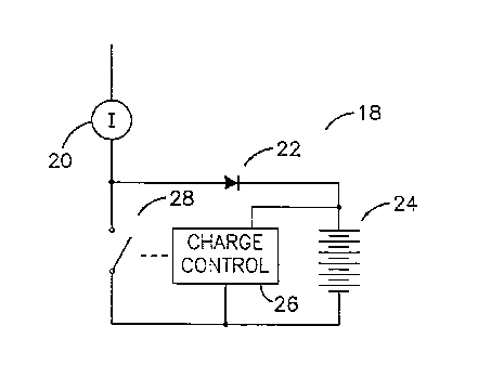
C-~ncid~ring now the disclosure of Figure 3 which
illustrates an idealized form of the present invention, the
basic t~ h;n~s of the invention can be contrasted to the
idealized charger of the prior art as shown in Figure 1.
In Figure 3, a circuit 18 is shown to be provided with an
ideal current source 20 having a single diode 22 disposed in
series in the circuit 18 between the current source 20 and a
battery 24. The diode 22 functions as a blocking device to
prevent discharge of the battery 24 when shunt switch 28
is conductive. Flow of current from the battery 24 is thus
- ~2~8a~95
blocked when current passes through the shunt switch 28.
It is to be understood that the diode 22 in an ideal
representation would best be shown as a polarity r~r~r~n~lent
switch. However, the salient point in this situation is
that the series pass element represented by the diode 22
is not a highly dissipative device and, in fact, negligible
losses result from the inclusion of the series pass element
represented by the diode 22 in the circuit even in the event
of a shorted output. A charge control 26 is also provided
in the circuit 18, the charge control function being provided
as commonly occurs through the use of an integrated circuit
(not shown). The shunt switch 28 is controlled by the charge
control 26, charge termination being effected in the
circuit 18 by the simple closure of the shunt switch 28.
In practice, the shunt switch 28 can take a variety of forms
including various types of transistor or thyristor. In
attainment of the objects of the invention, however, it is
necessary for the element comprising the shunt switch 28 to
function as a switch rather than as a variable impedance in
order to avoid unnecessary long term heating affects. Such
long term heating affects act to contribute to overall product
temperatures and to reduce reli~hil ;ty.
~ igure 3 essentially provides an idealized form
of a diode, that is, the diode 22, as a switch which works
in only one direction, that is, the switch provided by the
-- 10 --
~ 2180495
diode 22 is "on" when current flows to the battery 24 and
which is otherwise "off " . The shunt switch 28, which could
also be referred to as a charge control switch, can readily
be provided in discrete form through use of an SCR or a
transistor such as a field effect transistor, ~)LO~L hle
unijunction transistor or other transistors.
A consideration of Figure 3 leads to an appreciation
that different effective charge levels can be achieved simply
by operating the shunt switch 28 in an on/off duty cycle
pattern. Since a long period is more likely to be beneficial
in such a duty cycle pattern, it is not necessary to use high
frequency switching circuitry.
Referring now again to the prior art ideal charging
circuit of Figure 1, it is to be seen when also con~i~.oring
Figure 2 that a practical prior art implementation of the
idealized charger form of Figure 1 would include a voltage
source 30 which would best take the form of a step-down
transformer followed by a diode bridge 32 and an electrolytic
capacitor 34. While the transformer, bridge and capacitor
combination constitutes a common DC power supply, problems are
inherent to the utilization of the circuit elements as will
be described hereinafter. For the present discussion, it is
desirable to complete a view of the circuitry of Figure 2.
A series pass element is provided in the prior art circuit
of Figure 2 in the form o~ a transistor 36 in series with a
battery 38. Charge control 40 is, of course, provided in the
prior art circuit. - 11 -
- 2180495
The prior art charging circuit represented by the
circuitry of Figure 2 functions in a manner which is severely
deficient relative to the circuitry of the present invention.
A first problem of the prior art circuitry of
Figure 2 derives from input line voltage variation.
In essence, the secondary voltage of the voltage source 30,
that is, the transformer forming the voltage source 30, must
be sufficiently high so as to fully charge the battery 38 even
at low line. A higher voltage across the transistor 36, that
is, the series pass element represented by the transistor 36,
will result in a higher voltage at normal line voltages with
even higher voltage drops at high line. In order to counter
this undesirable affect, elaborate voltage regulation devices
would need to be used and would introduce substantial complexity
and cost to the prior art system of Figure 2.
The prior art system of Figure 2 inherently exhibits
a problem which becomes apparent upon an AC analysis of the
circuitry of Figure 2. With a sinusoidally varying AC input,
current will flow into the electrolytic capacitor 34 only
during the portion of the cycle when the secondary voltage
exceeds the voltage on the capacitor 34. Selection of the
form of the capacitor 34 then causes a tradeof~ to result
whereby a choice exists between a large electrolytic capacitor
which creates very short current pulses or a smaller capacitor
-- 12 --
~ 2~80495
having a larger conduction angle but which also provides high
voltage ripple. In any event, the resulting current waveforms are
reflected to the primary of the voltage source 30, thereby
producing an undesirable harmonic distortion with resulting
poor power factor. The f~t~rnRl power grid is impacted and,
internaLly of the circuit, an impc,ct is f:elt on the size of
tne voltage source 30 and/or the losseg associated with the
voltage source 3~.
The prior art circuit o~ Figure 2 exhibits other
problems associated with and inherent to the electrolytic
capacitor 34 and to the limited life of such a capacitor.
Line current distortions are also present in the circuitry
of Figure 2 since the se~ondary voltage must ex_eed battery
voltage in order ~or current to flow to the battery 38. 'i'nese
Ln~erent problems WLtn tne circuitry of Figure ~ rorce a
circult designer ~o encounter certal~l trqdeoffs since increasin~
the secondary volt~ge to achieve an Improv~d conduction angle
will result in increaseci losses in the series pa~s eleme~t
represented by the transistor 36.
1he transistor 36 in the circui~ry of Figure 2
cannot be operated as a swltch ~ut must operate as a variable
i--reA~n~-e. In the event that an attempt were made to operate
the transistor 36 as a switch, no current limit function would
be present in the circuitry to protect the circuit from output
_ 13 --
21 80495
shorts. While a current limited transformer could be provided
in the circuitry of Figure 2 as the voltage source 30 in an
effort to alleviate such inherent problems, substantial costs
and complexities are introduced by the incorporation of such
a specially constructed transformer, one of these costs being
losses in the transformer itself as well as the monetary cost
of devices of this nature.
Referring now to Figure 4, a practical implementation
of the idealized form of the present invention as shown
in Figure 3 can be appreciated particularly in view of the
problems inherent in the prior art circuit implementation
seen in Figure 2.
In Figure 4, a charging circuit 42 representing a
basic implementation of the present invention is seen to
operate on line voltage, the circuit 42 being arranged to
operate either on a voltage of 277 volts AC or 120 volts AC.
The respective voltage sources are conventional AC power mains
with an AC rated capacitor 46 being operative when the voltage
source is taken to be 120 volts AC while both AC rated capacitors
44 and 46 are operative for a line voltage of 277 volts AC. The
capacitors 44 and 46 provide ~ r~ nt constant current
source functions since losses associated with the capacitors
44 and 46 are very low. As previously described, the use of
transformers for voltage sources results in high operating
-- 14 --
2 1 80495
temperatures in a given system. Through the use of the
capacitors 44 or 46, temperatures do not appreciably rise
during operation.
In the charging circuit 42 of Figure 4, a bridge
rectifier 48 is provided in series with the capacitor 46 or with the
capacitors 44 and 46 and also with a series pass element 50 shown
in the drawing as comprising a diode operable in only one
direction. The circuit 42 also i nrllld~ the battery 52 which
is to be charged and a shunt switch 54 along with charge
control 56. The series pass element 50 is shown as taking
the form of a diode which is intended to function as a polarity
dependent switch in essentially the manner of the diode 22 of
Figure 3. The shunt switch 54 can take the form of a transistor
such as a programmable unijunction transistor or other device
as has been described hereinabove relative to the shunt switch
28 of Figure 3.
The voltage of the battery 52 is inherently low
as compared to the input AC voltage of the circuit 42, the
battery voltage representing a vectorial addition to the
capacitor voltage, that is, the voltage of either the capacitor
46 or the capacitors 44 and 46 deprn~;ng upon selection of the voltage.
Accordingly, the dif~erence in voltage across the
capacitors 44, 46 in any charge mode is slight or negligible.
The capacitors 44 and 46 thus have a function which can readily
be seen to constitute constant current sources since the
-- 15 --
2 1 80495
voltage across either the capacitor 46 or the capacitorS 44, 46
remains constant for all practical purposes. This negligible
voltage of the capacitor 46 or the capacitors 44, 46 also accounts for
certain inherent characteristics of the circuit 42, among
these characteristics being that the input current flows for
a large portion of the AC cycle. Further, eYen though power
~actor is leading, hA -n;C distortion is minimal in the
circuit 42.
In battery charging applications wherein the charge
level can be low and charge termination is not required, it
is recognized that capacitive impedance has previously been
utilized for battery charging, such as in the charging of
nickle-cadmium batteries. However, in the circuit 42, charge
termination and charge control are provided by the shunt
switch 54. As previously indicated, the shunt switch 54
preferably takes the form of a shunt transistor which functions
as a switch having a high ;mre~lAnce while the battery 52 is
charging and a very low impedance state to ef fect charge
termination. On/off duty cycle control can be readily provided
to produce int~ i Ate effective charge current levels between
the high charge level and ~ull charge termination. The shunt
switch 54 embodied in the form of a transistor can take various
forms consistent with intended circuit operation. Such devices,
when operated as switches, can be ~mho~; ed as relatively small
circuit elements which do not require the extensive heat
-- 16 --
2~80495
,
sinking of circuit components of the prior art since the
voltage drop across the shunt switch 54 is minimal.
Referring now to Figure 5, another embodiment of
the invention represented schematically in Figure 4 is seen
in a rearrangement of the circuit c~ ~on~nts of Figure 4.
Figure 5 thus provides a charging circuit 5 8 operable by
selection of AC mains voltages with capacitor 62 and capacitors
60 and 62 respectively acting as constant current sources
depending upon the selected voltage. The circuit 58 includes
a diode bridge 64 and a battery 66 along with a charge control
68 and a shunt switch 70 in the manner of the circuit 42 of
Figure 4. ~owever, series pass element 72 shown in Figure 5
as taking the form of a diode operable as a polarity dependent
switch is seen to be located in the circuit 58 in the return
path rather than the supply path as previously shown in the
charging circuit 42 of Figure 4. This circuit component
rearrangement does not materially alter circuit operation
even though the series pass element 72, that is, the diode,
has been moved to the return path of the circuit 68. As is
also seen in Figure 5, the shunt switch 70 is seen to be a
transistor shown as a PNP device. Operation of the charging
circuit 58 is identical to the operation oi the charging
circuit 42 of Figure 4.
-- 17 --
~ _ ~ 2 1 80495
Referring now to Figure 6, a charging circuit 74
according to the invention is seen to include a low voltage
switching converter 76. The circuit 74 overcomes a previous
limitation to the use of AC capacitors to provide a current
limiting function, the use of AC capacitors in prior art
situationS resulting in an increase in size with increased
charge current requirements. Accordingly, these prior
applications rec,uiring higher charge currents have utilizéd
transformers or off-line switching power supplies. In
situationS wherein the input must accommodate 277 volts or
voltages such as 347 volts, switching power supplies become
expensive, complex and more "lossy" due to increased onstate
resistance of the power devices and due to increased switching
losses caused by high voltage transitions. In contrast,
low voltage switching power supplies such as the converter 76
are simple and highly efficient. The combination in the
charging circuit 74 of Figure 6 of a capacitive input with
a low voltage switching power supply such as the converter 76
results in the ability to boost charge current by a factor
of lO without increasing AC capacitor size. A representative
converter 76 are those devices manufactured by National
Semiconductor Corporation under the trademark SIMPLE SWITCHER
and designated as Series LM1575/LMl575E~V/LM2575/LM2575ElV.
-- 18 --
21 80495
The step-down voltage regulators known as SIMPLE ~jW1L~ are
monolithic integrated circuits which provide all active
functions for a step-down switching regulator and are capable
of driving a lA load with P~c~ ont line and load regulation.
Either AC capacitor 80 or capacitors 78 and 80, d~r~on~l; ng upon
the selected voltage, function ag in the circuits of Figures
4 and 5. In the charging circuit 74, most of the input voltage
will appear across the capacitor 80 or the capacitors 78 and
80 since a vectorial addition exists of load voltage and
capacitor voltage in this circuit. In the charging circuit
74, application of an AC line voltage will result in a DC
voltage within bridge rectifier 82 which can easily reach 60
volts on capacitor 92 without materially affecting the voltage
on either the capacitor 80 or the capacitors 78 and 80.
Sizing of the capacitors 78 and 80 to deliver 100 milliamps
coupled with a voltage of 60 volts being present within the
diode bridge 82 results in 6 watts of power being delivered
to the input of the switching converter 76. Assuming at least
80% efficiency of the converter 76, then 800 milliamps can
be delivered to a 6 volt battery 84. The switching converter
76 acts in concert with inductor 86, Schottky diode 88 and
capacitors 90 and 92 within the circuit 74 for power conversion,
the inductor 86 being a standard coil which is readily available
as a discrete comro~nt. It is to be understood that the function
of the low voltage switching converter 76 could be provided by
discrete circuitry or to a desired degree of integration.
-- 19 --
21 80495
For simplicity, the SIrqPLE SWITCHER manufactured by the
National Semiconductor Corporation or a similar device
available from other manufacturers is chosen.
The charging circuit 74 in a manner similar to the
circuits described hereinabove relative to Figures 4 and 5
include a series pass element 94 and a shunt switch 96 as
well as a charge control 98. The elements of the circuit 74
of Figure 6 which are common with the circuit elements of
Figures 4 and 5 function in a manner similar to the functioning
of said common elements in the previously described circuits.
It is also to be understood that the switching converter 76
could be integrated into a charge controlled integrated circuit.
The operation of the charging circuit 74 of
Figure 6 is understood to have an input which is effectively
current limited by the AC capacitors 78 and/or 80 d~ppn~iing
upon the selected voltage. Since the input is current limited,
charge termination can be accomplished by clamping at a point
within the bridge rectifier 82. In the charging circuit 74,
it is preferred that the shunt switch 96 be turned on slowly
in order to prevent high current surges as the capacitor
92 is discharged. The particular circuitry
of the charging circuit 74 allows the attainment of high
charge levels without appreciably increasing the size of the
capacitorS 78, 80 and without incurring the losses commonly
associated with off-line high voltage switching power supplies.
_ 20 --
21 80495
Referring now to Figure 7, an improved emergency
lighting system is seen generally at 100 to incorporate the
charging circuitry of the invention with the system 100 being
particularly configured to oYercome long term operating losses.
The emergency lighting system 100 provides non-emergency lighting
through the use of exit lamps 102 operated in a non-emergency
mode by AC main power, the main power in the system 100 shown
being either 277 VAC or 120 VAC with the voltage being selected
for a particular application. As will be described hereinafter,
DC power is provided to exit lamps 104 through a battery 106
on failure of mains power. In the system 100, emergency DC
power from the battery 106 is used for exit marking through
the exit lamps 104 and for path of egress lighting through
"unit" DC lamps 108. Battery disconnect can be provided
through use of a plug 110.
The system 100 provides AC capacitors 112 and 114,
the capacitors 112 and 114 being utilized as a limited current source
when the 277 volt source is selected with the capacitor 114
being utilized as a limited current source when the 120 volt
source is selected. The capacitors 112 and 114 and
associated discharge resistors 116 and 118 as well as a
resistor 120 are combined in a discrete circuit element re~erred
to as box capacitor 122. The capacitors 112 and 114 act not
only to provide constant current sources as has been previously
described but also act to provide an effective voltage divider
_ 21 --
21 804q5
from which to operate the AC exit lamps 102 from the 277 voltage
source .
The 1, -;n;n~ circuitry of the system 100 can be
conveniently disposed on charger board 124 shown in the dotted
outline of Flgure 7. The circuitry on the charger board 124
includes diode bridge 126 and a shunt switch element which
takes the form of a programmable unijunction transistor 128.
The series pass element of the system 100 takes the form of
a diode 130 provided in the return path, the diode 130 acting
as a blocking device to prevent discharge of the battery 106.
An integrated circuit chip 132 constitutes an application
~peci~ic integrated circuit manufactured for the present
assignee by Xotorola, the chip 132 providing a number of
functions including a temperature compensated voltage reference
from which to accurately determine proper battery f loat
voltage. The integrated circuit chip 132 not only provides
the appropriate charge control function but also incorporates
logic which turns on the DC lamps 104 and 108 upon loss of
AC power and also prevents operation during installation
of the system 100 before building power is applied to said
system for the first time. Pin 9 of the integrated circuit
chip 132 connects to circuitry used to sense the presence or
absence of AC power and to accurately detect brownout
conditions. The circuitry includes diodes 134 and 136 as
well as resistor 138 and capacitor 140, the circuit elements
~ ~ 2 1 80495
134, 136, 138 and 140 acting as the "intelligence" which
tells the chip 132 whether AC power is applied from the AC
voltage sources. This circuitry also provides AC reset and,
if no power ls present, det~nm;nes whether power has been
applied for the first time. Switch 142 functions as a test
switch .
Transistor 144 connects directly to pin 7 of the
chip 132 and acts to turn on the DC lamps 104 and 108 which
constitute the emergency lighting of the system 100. The
transistor 144 is the only element of the system 100 which
could require a certain degree of heat ginking due to the
heavy loading represented by the lamps 104 and 108. The
transistor 144 only operates perio~l;cAlly and with limited
duration relative to the capacity of the ~attery 106, such
operation not being long term or continuous.
In Figure 7, the plOyL -hle unijunction transistor
128 comprises the switching function for shunt regulation
within the system 100. In Figure 8 which illustrates a further
emhodiment of the invention, transistors 146 and 148 provide
the switching function, the transistors 146 and 148 being
small, inexpensive transistors which take the form as
referenced in the art of T0-92 plastic transistors. The
diode 180 and diode 190 in Figure 8 are in the same current
path and are used to compensate for offsets present in the
-- 23 --
21 sa4qs
-
integrated circuit chip 182, which chip 182 is identical to
the chip 132 of Figure 7. It is to be understood that the
diodes 180 and 190 could be integrated onto the chip 182
thereby allowing the shunt switch comprised of the transistors
146 and 148 to be reduced to a single device. Similarly, the
shunt switch comprised of the transistor 128 in Figure 7
could be integrated onto the chip 132 due to vastly reduced
heat losses exhibited by the system 100.
In the system 100 of Figure 7, capacitors 152,
154 and 156 act to stabilize the circuitry of the system 100,
thereby providing a stable reference for stabilization of the
operating potential of the integrated circuit chip 132.
~hile this stabilization provided by the capacitors 152,
154 and 156 could be considered to be superfluous, it is
believed necessary to address the possibility of having the
battery 106 removed under power. Under such a condition,
the capacitor 192 would charge rapidly and the shunt device,
that is the transistor 128, would clamp the charge current,
thereby protecting the integrated circuit chip 132 from
excessive voltage. Optimization of the chip 132 for the
system 100 reduces flepon~lency upon electrolytic capacitors
even to the extent of replacement of the electrolytic capacitor
with a film capacitor due to the fact that an electrolytic
capacitor of a given size would no longer be necessary.
-- Z4
~ 2180495
-
The system 100 utilizes the capacitors 112, 114
as current limited sources in the preferred circuitry shown
in Figure 7. However, modification3 and adaptations of the
system 100 are possible within the scope of the invention.
As an example, a current limited transformer could be
utilized in the event that transformer isolation is desired.
A current limited transformer (not shown) could therefore
take the place of the capacitors 112 and 114. In such a
situation, operation of the shunt switch, that is, the
programmable unijunction transistor 128, remains identical.
In a likewise fashion, the switching function performed by
the transistor 128 could take other forms additional to the
form of a bi-polar transistor, examples of devices useful
for providing the low impedance path to the common return
are field-effect transistors, silicon controlled rectifiers
and the like.
Completing the circuitry of the charger board 124,
it is to be seen that diode 158 acts as a transient suppressor.
Diode 160 ~unctions as a high charge indicator, and the diode
150 can also be seen to indicate that power is in the "on"
condition. Resistor 166 constitutes an imre~n,-e ~or the
diode 160. When current flows through the diode 150,
current will flow through a parallel path which includes
resistor 162. Resistors 164 and 170 are provided in the
-- 25 --
21 80495
circuit for facilitating supply of the proper voltage and
gate current to turn on the pro~L ~hle unijunction transistor
128. Resistor 168 provides base current through the chip
132 to drive the transistor 144, which transistor 144 turns
on the DC lamps 104 and 108. The chip 132 also provides
a low battery detect circuit (not shown) which functions
as a low voltage disconnect to turn off the transistor 144
to prevent deep discharge of the battery.
Considering operation of the system 100, either
of the voltage sources 277 VAC or 120 VAC is selected for
operation of the system 100, the AC power coming from this
mains source then going through either the capacitor 112 in
the case of the 277 VAC or the capacitor 114 in the case of
the 120 VAC source. For the sake of simplicity, it will
be assumed that the 120 VAC source is selected. The 120 VAC
source directly drives the AC exit lamps 102 in the non-
emergency mode. Charging of the battery 106 also occurs
during at least a portion of the time during which the lamps
102 are operated by the 120 VAC source. When the battery
106 is not in a fully charged condition, the shunt element
represented by the programmable unijunction transistor 128
is in an "off " condition with DC current flowing from the
diode bridge 126 through the circuit to charge the battery
106. Battery charging occurs with the chip 132 looking at
-- 26 --
2 ~ 80495
the battery 106 through pin 5 to determine battery condition
with control occurring through pin 11. The transistor 128
is always either fully on or fully off but can move between
the on and o~f conditions after full charge in order to float
the battery 106. The transistor 128 is "off" during charge
and is "on" to float the battery 106 during which operation
the battery 106 discharges to a minor degree. The bridge 126
passes DC current to the circuit and through the diode 150
which preferably takes the form of a li.ght emitting diode
so that a visual indication is provided that the power is
"on". The resistor 162 bypasses at least some of the current
since the current in the circuit is too great for the diode
150 alone .
Full charge of the battery 106 is detected as
aforesaid, the programmable unijunction transistor 128, that
is, the shunt switch element, then turning on to connect
points 172 and point 174, thereby providing a bypass path
for current which does not include the battery 106.
The circuit 100 of Figure 7 can be configured
differently as referred to hereinabove as is seen in Figure 8
which illustrates a 8ystem 176 which is similar in many
respects to the system 100 of Figure 7. In the system 176,
the transistorS 146 and 148 function in the same manner as
the programmable unijunction transistor 128 o~ Figure 7.
-- 27 --
21 80495
In essence, the transistors 146 and 148 provide an "off "
condition for battery charging and turn on to provide a shunt
regulated path through which current flows when battery
charging is not desired.
Referring now to Figure 9, a simple charging circuit
200 is seen to be ~perable with two line voltage sources
with capacitors 202 and 204 operating as has been described
hereinabove. Diode bridge 206 also functions to rectify
AC current to DC current in the circuit 200 in a manner such
as is described hereinabove. Diode 208 functions as the series
pass element while a voltage ~eron~ nt switch shown generally
at 210 as comprising a silicon controlled rectifier 212
and a zener diode 214 acts to control charging and to
provide a shunt-regulated current path. The rectifier 212
functions as a shunt switch while the zener diode 214 acts as
a voltage sensing device to gate the rectifier 212, that is,
to cause the rectifier 212 to become conductive at a selected
voltage, thus turning the bypass path "on". The selected
voltage is that voltage at which battery 216 is fully charged
and at which the battery 216 is " floated" .
While the inYention has been described in relation
to idealized circuitry, several embodiments of simplified
practical circuitry and omho~ nts Of systems within which
the invention functions, it is to be understood that the
-- 28 --
- ~ 2~ sa4ss
invention can be configured other than as is expressly
described herein without departing from the intended scope
of the invention, the invention being limited only by the
recitations of the appended claims.