Note: Descriptions are shown in the official language in which they were submitted.
,~~ ~~~~3
IC COMMUNICATION CARD
BACKGROUND OF THE INVENTION:
Portable electronic devices such as notebook
computers are increasingly being provided with a slot for
receiving an IC card constructed in accordance with the PC
Card Standard which is jointly owned by PCMCIA (Personal
Computer Memory Card International Associates, 2635 N. First
St. Ste. 209, San Jose, California 95l34, U.S.A.) and JEIDA
(Japan Electronic Industry Development Associates, Kikai
Shinko Kaikan, 3-5-8 Shibakoen Minato-Ku, Tokyo 105, Japan.
Under such standards, each IC card has a card length of about
86 mm, a card width of about 54 mm, and a card thickness of
about 5 mm. A variety of IC cards are available, including
those with considerable memory so that data can be stored in a
card and the data transferred to or from the electronic device
and the card. The portable electronic devices may have other
input/output ports.
It is often necessary to transfer data between the
portable electronic device and a second device such as a
printer, desk top computer, etc. One technique for such
transfer is to provide an IC card with a connector at its rear
end, and a cable with one end that plugs into the card and
another end that plugs into the second electronic device.
Cables can be clumsy and inconvenient and are not preferred
for many of the same reasons that they are not generally used
to connect a remote television control to a television set.
Cables can be eliminated by connecting infrared emitter!
detector units through short cables to each of the two
electronic devices.
76132-18
~ a~~3
la
However, in the case of the first electronic device, which may
be a small portable computer, it can be annoying to have to
store such a unit with its cable and to separately support the
first electronic device and the unit. An infrared
communication system for connecting electronic devices, where
one of the devices has a slot for receiving an IC card, which
minimized efforts in storage and set up for infrared data
communications, would be of value.
SUMMARY OF THE INDENTION
In accordance with the present invention there is
provided a method for t ransmitt ing data between first and
second electronic devices, where each of said electronic
devices has a slot with a front end for receiving an IC card,
and has a device connector at the front end of its slot,
characterized by: constructing first and second IC cards that
are each insertable into one of said slots, that each has a
front card portion with a card connector, and that each has a
rear portion with a light emitter and a light detector;
insert ing the f ront card port ion of said first and second
cards, respectively into the slots of said first and second
electronic devices until each card connector and a
corresponding device connector are mated, with said rear card
portion of each card substantially projecting rearwardly out
of the corresponding slot;
orienting said elect ronic devices so the rear portions of
said cards generally face each other;
energizing the emitter of said first card so it emits
76132-18
lb
light modulated by data signals, and detecting said light by
the detector of the second of said cards.
In accordance with one embodiment of the present
invention, applicant provides a light communication capability
for an electronic device that is designed to receive IC cards,
which requires very little extra storage and which can be set
up very easily. Applicant provides an IG card with a front
port ion for
76132-18
C
WO 95119015 PCT/US95/00215
e80953
2
insertion into a card-receiving slot of the electronic device and with a rear
portion
which substantially projects from the electronic device and which carries a
light
emitter and/or a light detector. The emitter and detector are each mounted on
the same rigid frame of the IC card which projects into the slot, so the rigid
frame .
of the IC card maintains the emitter and/or detector in position and
orientation.
The light emitter and/or detector are each mounted substantially at the rear
edge
of the IC card and are oriented to emit light in primarily a rearward
direction away
from the card and to detect light passing in a primarily forward direction
towards
the rear of the card. The rear portion of the card preferably has about the
same
width and height as the front portion, which facilitates storage of the card.
Considerable light transmitting capability is obtained in the small card
thickness
by providing a plurality of light emitter elements that are spaced along the
width
of the card at substantially its rear edge.
The novel features of the invention are set forth with particularity in
the appended claims. The invention will be best understood from the following
description when read in conjunction with the accompanying drawings.
BRIEF DESCRIPTION OF THE DRAWINGS
Fig. 1 is a partial isometric view of an IC card and electronic device
constructed in accordance with one embodiment of the invention.
Fig. 2 is a plan view of the IC card of Fig. 1, with the cover removed,
and with some parts shown schematically.
Fig. 3 is a partial sectional side view of the electronic device of Fig.
1 and of an IC card constructed in accordance with another embodiment of the
invention.
Fig. 4 is a partial isometric view of an IC card constructed in
accordance with another embodiment of the invention.
Fig. 5 is an isometric view of a card and separate unit which can be
used in the device of Fig. 1.
Fig. 6 is an exploded view of an IC card of the prior art and of a
cable connector assembly mateable therewith.
WO 95I19015 . 218 0 9 5 3 pCT~S95100215
",",~.
3
Fig. 7 is a partial isometric view of an IC card and first electronic
device, shown in communication with a second electronic device.
Fig. 8 is an isometric view of the IC card of Fig. 7) with the top cover
removed.
Fig. 9 is an enlarged view of a portion of the IC card of Fig. 8.
Fig. 10 is a block diagram of circuitry of the IC card of Fig. 8.
Fig. 11 is a schematic diagram of emitter and detector driving
circuitry of the IC card of Fig. 8.
r ig. i r is a pariiai isometric view of two iC cards and two electronic
devices, each similar to those of Fig. 1, showing them in communication with
each other.
DESCRIPTION OF THE PREFERRED EMBODIMENTS
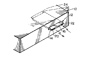
Fig. 1 illustrates an electronic device 10 and an IC card 12 lying in
a slot 14 of the electronic device. The IC card has a rear edge 16, projecting
from the electronic device. An infrared emitter 20 and an infrared detector 22
lie
substantially at the rear edge of the card and transmit and receive data. In
most
cases, the data to be transmitted is stored and/or generated in the electronic
device 10. The data is passed through a device connector 24 at the forward or
innermost end of the slot 14 to a card connector 26 at the front end of the
card.
That data is used to modulate the light output of the infrared emitter 20.
Similarly,
in most cases the data represented by modulation of the infrared light
detected
by detector 22 is converted into electrical signals which are transmitted
between
the connectors 24, 26 to circuitry within the electronic device 10. There can
be
cases where the transmitted and/or received data is stored in a memory chip
within the IC card itself.
Fig. 2 shows the IC card 12 with the card connector 26 at its front
end) with the emitter and detector 20, 22 lying at the rear edge portion 16. A
control circuit 30 controls the flow of signals representing data between
terminals
of the card connector 26 and the emitter and detector 20) 22.
4
Fig. 3 illustrates an IC card 40 which is similar to
that of Figs. 1 and 2, except that the card 40 has a rear
portion 42 which is of a thickness much greater than that of
the forward card portion 44 that fits into a slot of the
electronic device 10. The enlarged rear portion can be
helpful to accommodate larger emitters and detectors.
Fig. 4 shows a portion of another IC card 50,
wherein the rear edge portion 52 includes a cylindrical lens
54. The cylindrical lens 54, which 1s about half of a
cylinder, collects light lying above or below the horizontal
plane 56 of the card to provide more light for the detector,
and also directs light emerging from the emitter so it extends
more horizontally.
Fig. 5 shows a combination of an IC card 60) and
infrared transmit/receive unit 62, and a cable 64. This
arrangement provides an IC card 60 which can be stored in
storage compartments designed to receive "standard" IC cards.
However, the unit 62 and cable 64 require a separate storage
area. A case for holding a personal computer or other
electronic device and several standard IC cards, would have to
be built with a custom storage area for the unit 62 and cable
64. Also, when the combination of Fig. 5 is to be used, the
unit 62 with its inf cared emitter 66 and infrared detector 68
must be placed on a surface, and a weight or other holddown
may be required to position the unit 62 despite any sideward
urging by the bent cable 64. However, the combination of Fig.
5 has the advantage that the mechanical construction of the
76132-18
C
~~A~
4a
card 60 is similar to that of prior IC cards, which have
connectors at their front and rear ends. Fig. 6 shows such
prior card 70 which has mufti-contact connectors 72, 74 at its
front and rear ends. A cable assembly 76 includes a plug 78
that can be plugged and unplugged from the rear connector 74
of such card.
Fig. 7 illustrates a combination 80 of an IC card 82
and an electronic device 84 such a notebook computer. As
indicated in Fig. 8, the card 82 meets JEIDA and PC CARD
standards, which require that the card have a card length L of
about 86 mm, a card width W of about 54 mm, and a card
thickness T of about 5 mm. Fig. 7 shows the card 82 inserted
into a slot 84 of the electronic device and held in position
by slot guides 85. It may be noted that the front of
76132-18
C
WO 95I19015
PCT/US95/00215
the card has a front edge 87 of about 3.5mm thickness) while the rear of the
card
has a rear edge 89 of about 5mm thickness. These thicknesses are of about the
same magnitude because the smaller one (3.5mm) is more than 5096 of the larger
one. A front portion 86 of the card has a front card connector 88 that mates
with
5 an electronic device connector 90 that lies at the inner end of the slot. A
rear
portion 92 of the card projects from the slot. The rear portion has an emitter
and
detector which emit and detect infrared light, for communication with a unit
100
that is connected through a cable 102 to a second electronic device 104 such
as
a printer. The unit 100 and cable 102 are stored with the second device 104,
which is usually not portable, so the bulk of the unit 100 is usually not a
significant disadvantage. The unit 100 has a considerable thickness to
accommodate a relatively large emitter 106 and detector 108.
Fig. 8 illustrates the IC card 82) wherein a top cover 110 (Fig. 7) has
been removed. The card includes a rigid frame 112 with a frame front 114 on
which the front card connector 88 is mounted) and with a frame rear 116. A
light
emitter 120 and light detector 122 are mounted (indirectly) on the frame, so
that
the emitter and detector are fixed in position and orientation with respect to
the
rigid frame 112.
The card 82 includes a circuit board 130 with electronic components
132 mounted thereon. The circuit board has a front end 134 with traces (not
shown) to which tails 136 of contacts of the front card connector 88 are
soldered.
The circuit board also has a rear end 138 with traces to which the emitter 120
and
detector 122 are connected.
The emitter 120 is formed by four emitter elements 141-i44. The
frame has a rear barrier 150 at its rear edge) with the rear barrier lying
immediately rearward of the emitter elements. The rear barrier has a plurality
of
. holes 152 aligned with the emitter elements to pass light in a generally
rearward
' direction from the emitter elements. A infrared window 154 is placed
immediately
' rearward of the infrared detector 122 to pass only infrared light, and
thereby block
WO 95I19015 PCTlUS95/00215
2180953
6
visible light and other frequencies that will tend to overload the detector
122. The
detector 122 is oriented to detect light moving in a forward direction F
towards
the rear of the card. '
Fig. 9 illustrates one emitter element 142 and a portion of an
adjacent emitter element 141. The emitter element such as 142, is an off-the-
shelf
item that includes a pair of terminals 160, 162 and a light emitting chip 164,
all
embedded in transparent plastic that includes a ~nc-entrating lens 166. The
holes or openings 152 in the rear barrier 150 are of largely conical shape,
and
limit the emission of light so it is within a conical beam having a spread
angle A
of about 40 degrees (20~ to 80~) around a forward-to-rearward axis 170 (about
20~
above and 20~ below). The rear barrier 150 also includes an opaque separator
172 on laterally (direction B) opposite sides of each light emitting element,
to
block any light from passing through an opening lying in front of a different
element. Such separators block light from reaching other detectors of other
devices in the vicinity, and generating noise in them.
Each emitter element is mounted and electrically connected by
soldering its leads 160) 162 to corresponding pads 180, 182 at the rear end
138
of the circuit board 130. The barriers 172 only generally position the emitter
elements. If an emitter element should be mounted in large misalignment with
the axis 170 of a corresponding opening 152) then some light from that element
will be blocked) and will not interfere with detectors of other electronic
devices in
the immediate environment. The fact that there are a plurality of different
emitter
elements, results in high assurance that there will be light transmitted
throughout
the intended conical beam of angle A. This allows communication with a known
degree of misalignment between the emitter and detector elements of the two
electronic devices. The provision of a plurality of emitter elements that are
laterally spaced in direction B (parallel to the width W of the card) enables
the '
rear portion of the card to have about the same thickness as the front
portion)
while still enabling considerable light energy to be transmitted. Such small
thickness at the rear end enables the card to be easily stored in storage
equipment intended for storage of other IC cards of the "standard" JEIDA and
PC
WO 95I19015 _ 218 0 9 5 3 pCT~S95/00215
7
CARD shape and size. It is desirable that the width W and length L each be
within 1596 of JEIDA and PC CARD standards (86mm and 54mm, respectively)
and that the thickness T be within 5096 of JEIDA and PC CARD standards, to
enable the card to be stored in space intended for storing "standard" IC
cards.
Fig. 10 is a block diagram of the electronic circuitry of the IC card
of Fig. 8. Data is transmitted in eight bit parallel format over eight lines
between
the electronic device connector 90 and the card connector 88 to an
input/output
circuit 190 which changes its parallel input at 192 to a serial output at 194.
Signals representing data on line 194 are delivered to a digital control 200
which
formats the signals) as by generating appropriate signals at the start and
stop of
a data transmission, as well as to convert the digital data on line 194 to
serial
analog data on an output line 202. The signals on line 202 are delivered to an
analog driver 204 which amplifies the signals and uses them to drive an
infrared
input/output 206 that includes the transmitter 120 and detector 122. The
energy
delivered over line 210 generates modulated infrared light which is
transmitted as
indicated by arrow 212. Light received as indicated by arrow 214 is detected
by
the detector 122 of circuit 206 which delivers its output on line 214 to an
amplifier
215 which amplifies the signal and delivers it over line 216 to the controller
200.
The controller 200 generates data representing the modulation of the detected
infrared beam and delivers it over line 196 to the input output circuit 190.
The
circuit 190 delivers the data in parallel form to the electronic device.
Fig. 11 illustrates details of the analog driver 204. Signals delivered
over line 202 pass through a f tter portion 220 to an amplifying transistor
230.
Direct current power from a line 232 passes through the four parallel-
connected
emitter elements 141-144 to energize these elements and cause them to emit
infrared light in synchronism (the modulation is in synchronism). The infrared
detector 122 has its output delivered to an amplifier 240 which delivers its
output
through a line 216. The circuitry of Figs. 10 and 11 are known in the prior
art,
and are presented only to provide an example of circuitry useful to energize
the
emitters and detectors of the. IC card.
WO 95l19015 ' ~ ~ $ 0 9 5 3 PCT~S95/00215
8
Fig. 12 illustrates a setup 250 'where the IC card 82 that lies in a slot
of an electronic device 10) is communicating with another substantially
identical
IC card, or IC card element 252 that lies in a slot 254 of another electronic
device .
or instrument 256. The instrument 256 is shown as another compact portable ,
one such as a notebook computer. The IC card element 252 has an infrared '
emitter 260 comprising four emitter elements and an infrared detector 270
which
faces in a rearward direction R2 with respect to the instrument 252. The use
of
two IC cards or card elements to establish data communication between two
electronic devices or instruments that each have a card receiving slot 84)
254,
i 0 makes communication especially convenient and at low cost.
Thus, the invention provides an IC card with a front portion for
insertion into a slot of an electronic device, and a rear portion that
substantially
projects from the electronic device and that carries a light emitter and/or
light
detector. The IC card has a rigid frame, and the emitter and detector are
fixed
in position and orientation on the frame. It may be noted that while Fig. 8
indicates a frame 112 which is of molded plastic material, it is possible to
construct the card with a rigid frame formed by metal) which may be in the
form
of metal halves that form metal top and bottom covers and metal sides and that
are fixed to the card connector and or ends) of the arcuit board or mounts
thereon. In any case) the frame forms a rigid structure that positions the
front
card connector 88 and the emitters and detectors. Although it may be possible
to adjust the. orientation of the emitter and/or detector) once adjusted they
are
held in a fixed position and orientation with respect to the electronic device
that
forms the card-receiving slot) by the rigid frame. This allows a person to
begin
infrared communication by inserting applicant's IC card with emitter and
detector
capability, into a card-receiving slot. Thereafter, the electronic device)
through the
rigid frame of the card) supports the emitter and detector and fixes their
position
and orientation. Although it is possible to mount batteries in the IC card, as
where the card has an enlarged rear end as shown at 42 in Fg. 3) electrical
WO 95I19015 218 0 9 5 3 p~~s95/00215
9
energy is generally provided by the electronic device through the connector
interface formed by the device connector and the card connector at the front
end
- of the card.
Applicant obtains increased infrared light transmission by the use
of a plurality of lateraiiy-spaced emiiiing eiemenis lying near the rear edge
of thG
card. This allows applicant to use small off-the-shelf emitter elements that
are of
small enough size to fit into the card rear end where it is about the same
thickness as the front portion, and still obtain a large light output.
Although it is
possible to transmit light in the visible spectrum, this is generally
undesirable)
, partially because of interference from visible light in the environment.
Applicant
prefers to transmit and receive infrared light, of a wave length of about 950
nanometers. The emitters lie at the rear edge portion of the card and transmit
light primarily in a rearward direction. The light detector similarly detects
light
passing primarily in a forward direction towards the rear edge portion of the
card.
A plurality of laterally-spaced detector elements can be placed near the rear
edge.
Although particular embodiments of the invention have been
described and illustrated herein, it is recognized that modifications and
variations
may readily occur to those skilled in the art, and consequently) it is
intended that
the claims be interpreted to cover such modifications and equivalents.