Note: Descriptions are shown in the official language in which they were submitted.
PC 672 ~ 8 ~
WAVELENGTH-DIVISION MULTIPLEXING TELECOMMUNICATION SYSTEM
AND METHOD PROVIDING A CONTROLLED SEPARATION OF THE OUTPUT
CHANNELS
Description
5 The present invention relates to an optical telecommunication system and method
particularly Cl,U,UlU,Ulid~ for ..~v~l~.,utl,-division multiplexing (or WDM)
lldllolll;~:~iull, in which the different channels are recognized and separated on
reception.
1û For a ~ I.,.,y,tl,-division multiplexing or WDM lldllollli~oiO~, several channels,
that is several lldllOlll;OD;OII signals il1de~el1d~"1 of each other, are required to be
sent over the same line consisting of an optical fibre by multiplexing in the domain
of optical Wî ~ ytllo, the Lldllol,litltd channels can be both digital and analog
and are distinguisable from each other because each of them is associated with aspecific wavelength, separated from that of the other channels.
In order to transmit a high number of channels making use of the so-called thirdlldl~OllliOOiUII window of the silica-based fibres and the useful band of optical
amplifiers, the w~v~l~.lytl, separation between the channels cull~ llLly is in the
2û orderof nd,,ur,,t:L~ ,O.
For a correct reception of such ll~llolllioo;ul~ signals it is therefore necessary to
cany out a separation between the channels ll~,"~ ver SO as to convey them to
the respective users.
To this end, optical nanrow-band filters can be used through which the selected
channel alone can pass, so as to ensure the absence of undesired signals that
would constititute a noise if superposed with the selected channel.
However, for the use of such filters both a high wavelength stability of the
3û 1, dl 10111"' ' signal and a high intrinsic stability of the f Iter passband is required.
This problem is described for example in patent application GB 226û046 in which
it is suggested to superimpose a pilot signal with the data to be t~d~:.",ilL.:d, by
detection of which pilot signal the filter passband can be adjusted.
2~12i~
PC 672 - 2 -
ln addition, known optical filters suffer from slip problems, based on which a
selected ~ n~l, for a passband keeps constant only over a limited period of
time after setting; said hlters, in particular in the case in which they are provided
5 with pit ~ , actuators or the like, are also subjected to hysteresis
u",~nd, based on which the selected passband h_.~ .lyLII value depends
not only on the value of the related control quantity (a volta3e for example), but
also on the time law through which said quantity is applied to the filters.
US Patent 4973124 in the name of K. Kaede, discloses, among other things, a
device for addition and drawing-off or bleeding oF ~ c:~""ined ~.J~ .iy~
to/from a .._~ y~ multiplexed signal ~." r _ ' ,9 along an optical fibre. In oneversion the device is comprised of two puld~i~dlio~l splitters, one quarter-waveplate and a first and a second Bragg-grating optical filters having the same Bragg-
15 ..~ .ly~l,; from a plurality of signals at different .._~ .,y~ the device enables
one single signal at the filters' Bragg ~ y~l, to be added or bled.
US Patent 4740951, in the name of J. Lizet et al., describes an integrated-optics
device to demultiplex n light signals of different wavelengths forming a light beam
20 transmitted from a first optical fibre towards n second optical fibres. The device
comprises n Bragg-gratings disposed in cascade. The cascade a" dl Iy~., 11~:11
involves a differential attenuation between the signals, by effect of the passage
through a different number of Bragg-gratings, depending on the ~ y~ll. At
each of the n Bragg-gratings in integrated optics, in addition, an ap~,,.".,id~
25 focusing optics of the ~io"t:~,u"di"g signai diffracted towards one of the second
optical output fibres is necessary, which will involve a very ~ device.
In one aspect, the present invention refers to an optical telecommunication
method comprising the steps of:0 - generating at least two optical ~Idll~ kJI~ signals, at pl~dcle:illl;ll~d
y~l 1 7 different from each other;
' ~' PC672 -3~ ~1~12~
-division multiplexing said optical signals in a single lldll~ C.;~/II
fibre, formins a ml 1"' ~:~nv^'-~gth optical signal comprising said optical
lldllDlll;;~siOI~ signals;
--I,d"-",illi"g said nl~ " wa~ yll, optical signal through said optical fibre to a
5 receiving station;
--feeding said m~" w~vclcngth optical signal comprising said optical
lldll;~ iUI~ signals to a respective receiving unit in said station;
--receiving the nl~" wa~lclcngth optical signal in said receiving unit;
-- separating said optical lldll~lll;Di~iOI~ signals and feeding them to respective
1 0 receivers,
in which said step of separating said Lldlli~u;__;JIl optical signals comprises:- splitting the received ml~" vlav~ l, optical signal onto at least two output
fibres;
- in at least one of said two fibres, selectively reflecting one Wl-V~ 1 1 band of
15 said n~ lcngth optical signal, said band having a width compnsing at
least one of said optical lla~ .ul~ si3nals, so that said reflected band
~ u,uau~ over said output fibre in an opposite direction to said multi-
wavelength optical signal;
--separating said band reflected from said output fibre and feeding it, through a
20 receiving fibre, to a respective receiver.
Preferably, said step of splitting said received nl~'f~ Lll optical signal
comprises splitting said signal onto several output fibres the number of which is
the same as that of the optical 1, dl 1~11 lii~i~;ull signals.
Preferably, said sek~ ly reflected wavelength band comprises one alone of
said lldlli~lll;__;UII channels.
In a particular ~lbudi~clll of the present invention said reflected v~,~
30 band has at least a 2 nm width, more particularly a 5 nm width.
Preferably said step of splitting the multi . ~ l optical signal Cull'~.ll,uldl~:s
separating said signal into ,ul~,dt~ ",i"ed fractions.
PC 672 - 4 ~
Preferably said step of separating said reflected band from said output fibre
comprises separating a ,u,t:d~ ",;,l~d signal fraction, in particular 50%
5 In a second aspect, the present invention refers to an optical telecommunication
system cu" ,u, i~;"y.
- an optical-signal llailsl~ llg station comprising means for generating
l,d,~s",;~,ion signals at at least two ~,~d~ ""i"ad wavelengths, and
wavelength-division multiplexing means for said lldll::~lll;SS;UIl signals, on a10 single optical-fibre line;
- a receiving station for said optical signals,
--an optical-fibre line connecting said lldll~ lill9 and receiving stations,
in which said optical-signal receiving station comprises means for selectively
separating said lldll:~lllis~liUII signals from said single optical-fibre line, which
1 5 comprises:
--one signal splitter, adapted.to divide the optical input signal onto several optical
outputs;
--at least one ..~ I,-selective reflector, having a reflected band comprising
at least one of said ~,,e.lt~l~""i"ad .._~ lls and connected with one of said
20 optical outputs;
- a second signal splitter connected with said selective reflector and adapted to
receive said reflected band and divide said reflected band onto two outputs
according to ,~ delt:""i"ed ratios;
--an optical receiver connected with one of said outputs of the second signal
25 splitter.
Preferably, said first and second signal splitters are non wavelength-selective
splitters; in particular, said second signal splitter can be a directional coupler, in
particular having a 50% division ratio
In particular, said selective reflector is a Bragg-grating reflector of a fixed pitch or,
preferably, of a variable pitch
PC672 ~ ~ 2181~1~
According to alternative versions, said selective reflector has a reflected band of at
least 0.3 nm, or at least 2 nm, around a ~ dt~ d central ~ .
depending on the features of said ~, dl IDI I ~;SSiUI ,-signal generating means.
5 Preferably, said central ~ elc,lytll of said selective reflector COII~:D~JUIICID to the
central emission wavelength of at least one of said ~,d,,D,,,;Da;u,,-signal generating
means.
In particular, said selective reflector may comprise heat control means.
Preferably, said selective reflectors are of the same number as said ~IdllDlllisDiu
channels.
In a further aspect, the present invention relates to an optical ~ .Iy~ selective
15 receiving unit comprising means for the selective separation of wavelength-
division mll~ y ~la"D",;~J;o" signals, which comprises:
- one signal splitter, adapted to distribute an optical input signal on several
optical outputs;
- at least one wav~!~, Iytl ,-selective reflector, having a reflected band comprising
20 at least one ~A~a~ .ly~l of one of said signals connected with one of said
optical outputs;
-- a second si3nal splitter connected with said selective reflector and adapted to
receive said reflected band and divide said reflected band onto two outputs
according to ~ e" " ,i"ed ratios;
25 - an optical receiver connected with one of said outputs of said second signal
splitter.
Preferably, said first and second signal splitters are non ~ !u"ytl,-selective
splitters. In particular, said second signal splitter can be a directional coupler, in
3û particular with a 5û% division ratio.
In particular, said selective reflector is a Bragg-grating reflector.
' ~' PC672 -6- 218~21~
According to alternative versions, said selective reflector has a reflected band of at
least 0.3 nm or at least 2 nm, around a ~JIedele~ èd central v~.~'~"yLl"
depending on the features of said ll dl l;>lll;~ iUI I signals.
5 In particular, said selective reflector may comprise heat control means.
Preferably, said selective reflectors are of the same number as said lldl~SIII;~,C~;JII
channels.
10 More details will become apparent from the following description, with reference to
the ac~.u~ a~ g drawings, in which:
--Fig. 1 is a diagram of a mll~ v/a~clcngth telecommunication system according
to the present invention;
- Fig. 2 is a diagram of a line amplifier for use in the system of Fig. 1;
15 --Fig. 3 is a spectrum of the detected signal at the multiplexer output port of the
lldllDlllit~illy station in the system of Fig. 1;
- Fig, 4 is a spectnum of the detected signal at the pre-amplifier output port in the
system of Fig. 1.
20 a) System description
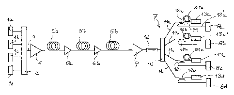
As shown in Fig. 1, an optical ~ .,y~ division mll ~ y multi-channel
telecommunication system according to the present invention colltclll~Jld~tls
several optical-signal sources, four for example, denoted in the figure by 1a, 1b,
1c, 1d le:~ue~ ly and having wave~engths ~ 3, ~ included in the useful
25 work band of the amplifiers disposed in succession in the system.
Said optical signals are fed to a signal combiner 2, or multiplexer, adapted to send
the signals at ~" ~, ~3, ~, simultaneously over a single optical output fibre 3.
30 In general, the signal combiner 3 is a passive optical device by which the optical
signals lldl~,lllilled over respective optical fibres are superposed on a single fibre;
devices of this type consist for example of fused-fibre couplers, in planar optics,
l~lk,luu,uli~ and the like.
PC 672 - 7 - 2
. ~
By way of example, an d,U,UlU,Ulid~: combiner is combiner 1x4 SMTC-0104-1550-
A-H c~""l,~luidli~d by E-TEK DYNAMICS INC., 1885 Lundy Ave, San Jose, CA
(USA).
Through fibre 3 said optical signals are sent to a power amplifier 4, which raises
the signal power to a value suffcient to enable said signals to travel over a
subsequent optical fibre portion extending before other amplifying means, while
Illaill~di"i"~ the required ~Idll:>lll;__ lC quality.
Thus, connected with power amplifier 4 is a first portion 5a of optical line usually
consisting of a single-mode optical fibre of the step index type, which is introduced
into an d,U,UlU,Ulid~t: optical cable having a length of some ten (or hundred)
kilometers; said cable is for example about 100 kilometers long, with the
15 amplifying means described below and the stated power levels.
In some cases, also optical fibres of the dispersion shifted type can be used.
At the end of this hrst portion 5a of optical line there is a first line amplifier 6a,
20 adapted to receive the signals, attenuated during their travel over the fibre, and to
amplify them to a sufficient level to enable them to be fed to several successive
portions of optical line 5b, of the same features as the preceding one, and to the
related line amplifiers 6b (in the figure, for the sake of graphic simplicity only two
optical fibre portions 5b and one amplifier 6b are shown), thereby covering the
25 overall ~Idll:~lll;ssiUII distance required for reaching a receiving station 7 in which
the signals are splitted, depending on the different ~Idll~ d channels identified
by the respective ~ , and sent to the respective receivers 8a, 8b, 8c, 8d.
The receiving station 7 comprises a pre-amprfier 9 adapted to receive the signals
30 and amplify them c~ ,uel l~d~ for losses given by the subsequent demultiplexing
apparatuses, until a~ ",t~ of a power level d,U,UlU,Uli~.~, to the sensitivity of
the receiving devices.
PC 672 - 8 - 2 ~ 1 8
From pre-amplifier 9, signals are sent to a device adapted to split the optical
signals fed to an input fibre onto several output fibres, separating them in relation
to the respective wavelengths; this device, also referred to as demultiplexer,
consists in the example herein described, of a fused-fibre splitter 10 separating
the input signal into signals on several output hbres, four in this case, each of said
signals being fed to respective fibres 11a, 11b, 11c, 11d, for connection with the
respective receivers 8a, 8b, 8c, 8d.
For example, for splitter 10 a component of the same type as the already
described signal combiner 2 may be used, mounted in an opposite configuration.
Fibres 11a, 11b, 11c, 11d are connected, through respective directional couplers1 2a, 1 2b, 1 2c, 1 2d to selective-reflection filters 1 3a, 1 3b, 1 3c, 1 3d.
The receivers 8a, 8b, 8c, 8d are connected with a respective fibre coming out ofthe directional couplers 12, receiving the reflected signal from the respective
selective-reflection filters 1 3a, 1 3b, 1 3c, 1 3d.
An optical isolator 14 is interposed between the pre-amplifier 9 and splitter 10.
Optical isolator 14 is preferably an optical isolator of a type iln~i~,el1d,:"t of the
pUIdli " ~ of the ~Idl~ .ll signal, of an isolation greater than 35 dB and a
reflectivity lower than -50 dB.
Appropriate isolators are for example model MDL 1-15 PIPT-A S/N 1016 available
from ISOWAVE, 64 Harding Avenue, Dover, New Jsersey, USA.
The directional couplers 12 preferably are fused-fibre couplers 50:50 adapted toseparate into even parts, in the output fibres, the optical power fed to an input
fibre; an d,U~ Jlidtt: coupler is model SWBC2150PS210, manufactured by E-TEK
DYNAMICS INC., 1885 Lundy Ave, San Jose, CA (USA).
?1~2~
PC 672 - 9 -
The s~vle~ c ~vtl~vtiu,- filters 13 preferably are ûf the same number as the
~Idll~",itl~d channels and each reflect a wavelength cv"~,,uullvi"g to one of said
channels.
Selective-reflection filters preferably adapted for use in the present invention are
r/~vcguide distributed-Brag3-grating filters which reflect the radiation in a
narrow ..~ . Iy~l, band and transmit the radiation to the outside of said band.
Said filters consist of a portion of an optical waveguide, an optical fibre for
1û example, along which the refractive index has a periodic variation and at said
index variation there is a partial signal reflection: if the signal portions reflected at
each index change are in timed " ' ' ,~1 ,i,u with each other there is a constructive
i"l~,r~ "ve and the incident signal is reflected.
15 The constructive i"lr,,f~ ,ce condition, cv"~s,uul,vi,~g to the reflection maximum,
is expressed by the relation 21 = AJn, wherein I is the ,qrating pitch fonmed by the
refractive index variations, ~ is the ~ ,lytll of the incident radiation and n is
the refractive index of the optical waveguide core. The descnbed ~I,ellv",~"u" is
known in literature as distributed Bragg reflection.
2û
The periodic variation of the refractive index can be achieved by known
techniques, for example by exposing one optical-fibre portion deprived of the
protective polymeric coating, to the i"t-v,r~ "c~ fringes formed by an intense UV
beam (as the one generated for example by an excimer laser, a frequency-
25 doubled argon laser or a frequency-quadrupled Nd:YAG laser) which is caused to
interfere with itself by an d,lJ,UlU,Ulid~ tllr~:lU111~5r system, by a silicon phase
mask for example, as described in US Patent 5,351,321.
The fibre, and in particular the fibre core, is thus exposed to a UV radiation of a
3û pv. iuviv~ varying intensity along the optical axis. In the core portions reached by
the UV radiation of the greatest intensity a partial breaking of the Ge-O bonds
occurs, which will cause a permanent ", " ' ~ of the refractive index.
PC 672 - 10 ~
By selecting the grating pitch such that the constructive i"~, r~,c "~ relation can
be verified, the centre v.~v~ of the reflected band can be d~ "";"ad at will,
following known criteria.
5 By this technique it is possible, for example, to produce filters having a reflected
wavelength band at -3 dB, typically of 0.2 - 0.3 nm, reflectivity in the middle of the
band until 99%, central wavelength of the reflected band sl lccertihle of
""i" " , during the manufacturing step within about i O.1 nm and variation of
the central band ~ . Iutl ~ at a temperature as low as 0.02 nm/C.
For example, for a modulated lldll~lllissiu,, at 2.5 GbiVs, with an external-
modulation source, at a known central emission ~ ly~ll, to be d~lellllill~d for
example at less than 0.01 nm, a total band of about 5 GHz is needed and a band
of at least 10 GHz, cul, ~ ol1di, ,9 to about 0.1 nm, is required from the grating.
Taking into account a tolerance in the central wavelength of the reflected band in
the grating of about 0.1 nm, a iull~,uull.lillg minimum bandwidth for the grating is
at least 0.3 nm.
20 This value can be achieved by fixed-pitch gratings.
Should the wavelengths of sources 1 a, 1 b, 1 c, 1 d have a wider tolerance interval,
the availability of filters with a passband of cu,,c:~l,ulldill~a width will be convenient,
in order to include the source emission length within the band reflected by the
25 filters.
In the case of sources consisting of a semiconductor laser of a cu,,,,,,c,~ 'y
available type, for example typically having a known emission wavelength at lessthan i 1 nm (obtained by laser selection), it is possible to make optical-fibre
30 distributed-Bragg-grating filters with a suflficiently large bandwidth in reflection by
imposing a variable pitch to the grating, thereby making a so-called chirped
grating.
2~21~
PC 672
For the purpose known techniques can be used, as taught for example in an
article by P.C. Hill et al, published in Electronics Letters, vol. 30, No. 14, 07/07/94,
pages 1172-1174.
5 Gratin3s of the above type are for example ~vu,,,,l,v.vidli~vd by PHOTONETICS
Inc., Wakefield, MA (USA), for the desired reflection wavelengths.
To the purposes of the present invention, when not othenwise specihed, for
emission wavelength of a laser source it is intended a ~ yLll band, of
10 ,u, v,v~v~v,,,,;,,ed width, centered around a central emission wavelen3th. Said central
lyLI~ is generally selected based on the same constructive tolerances as
adopted in selecting vu"",.v,~ 'ly available lasers.
To the purposes of the present invention and for the above described use, the
15 power ampllfier 4 is for example an optical fibre amplifier of a cu~ l;vlvidl type
having the following features:
input power -13.5 to -3.5 dBm
output power 12-14 dBm
work .vlvlv.ly~ll 1530-1560 nm.
An d,U,UI U,UI i ' model is for example TPA/E-MW, marketed by the Applicant.
Said power ampliher uses an erbium-doped active optical fibre, of the type
described below.
By power amplifier it is intended an ampliher operating under saturation
conditions, in which the output power depends on the pumping power, as
described in detail in the European Patent No. EP 439,867, herein ill~vUl~UUldLed by
reference.
To the ends of the present invention and for the above use, by pre-amplifier it is
intended an ampliher put at the line end, capable of increasing the signal to be fed
to the receiver to a value cu"~ v":ly higher than the receiver's sensitivity
threshold (for example in the case of a lldll-vlll;_v;vl~ at 2.5 GbiVs, to such a value
PC 672 -12 - 21 ~
.
that the power reaching the receiver be included between -26 and -11 dBm), whilesimultaneously introducing the lowest possible noise and keeping the signal
e~ 7Afinr~.
5 Pre-amplifier 9 is, for example, an optical fibre amplifier of a col"",e,~:.,l'y
available type, having the following features:
overall power input -20 to -9 dBm
output power 0-6 dBm
work .~a~ "~l, 1530-1560 nm.
An d,U,UlUplid~t: model is, for example, RPA/E-MW, c~"""~,uidli~d by the
Applicant.
Said amplifier makes use of an erbium-doped active optical fibre of the type
15 described later on.
The conhguration of the above-described Lldll~ kJII system appears to be
particularly djJ,UlUUliCII~ to provide the desired pt:lrUlllldll~, in particular for
"~tl,-division multiplexing lldllDlll;~ over several channels, in the
20 presence of a particular selection of the properties of the line amplifiers being part
of it, above all as regards the capability of tldils",i~li"y the selected ..a~ "~l,s
without some of them being penalized as compared with others
In particular, a uniform behaviour for all channels can be ensured, in the
wavelength band included between 1530 and 1560 nm, in the presence of
amplifiers adapted to operate in cascade, making use of line amplifiers which are
provided for having a substantially uniform (or "flat") reply to the different
wavelengths, in a cascade operation
b) Line amplifier
For the above purpose, an amplifier provided for use as a line amplmer, can be
made following the diagram shown in Fig. 2 and it comprises one active fibre 15,doped with erbium, and a related pump laser 16, connected therewith through a
dichroic coupler 17; one optical isolator 18 is disposed upstream of the fibre 15, in
.. ... . .
2~8i~
PC 672 - 13 -
the travel direction of the signal to be amplified, whereas a second optical isolator
19 is disposed '~ dlll of the active fibre.
In the case of a two-stage ~IIIb~-lilllelll, the amplifier further comprises a second
erbium-doped active fibre 20 associated with a cu"~,uul,~i"g pump laser 21 via a5 dichroic coupler 22, which also is connected for countercurrent pumping in theexample shown; ~ dlll of fibre 20 there is therefore another optical isolator
23.
The pump lasers 16, 21 are for example lasers of the Quantum Well type, having
10 the following features:
emission wavelength ~p = 98û nm;
maximum optical output power Pu = 80 mW.
Lasers of the above type are manufactured for example by: LASERTRON INC.,
15 37 North Avenue, Burlington, MA (USA).
Dichroic couplers 17, 22 are in this example fused-fibre couplers, formed of single-
mode fibres at 98û and within the wav~ u,tl, band of 1530-156û nm, with a
variation < 0.2 dB in the optical output power, depending on pold, i~d~iUI~.
Dichroic couplers of the above type are known and available on the market and
are produced, for example, by GOULD Inc., Fibre Optic Division, B~j", 'û~
Drive, Glem Burnie, MD (USA), and by SIFAM Ud., Fibre Optic Division,
Woodland Road, Torquay, Devon (GB).
Optical isolators 18, 19, 23 preferably are optical isolators of a type il,d~,ua~,dt:"l of
the pUldl i~d~iUI I of the 1, dl ~ ;UI~ signal, with an isolation greater than 35 dB and
a reflectivity lower than -50 dB.
30 Appropriate isolators are for example model MDL-1-15 PIPT-A S/N 1016 available
from ISOWAVE, 64 Harding Avenue, Dover, NJ (USA).
PC672 -14- 21 8~2~`~
.
In the described system the line amplifiers are provided for operation with an
overall optical output power of about 14 dBm, with a gain of about 30 dB.
In the diagram shown in Fis. 1 the two stages of the line amplifier are disposed in
5 a counter-,u,updyd~ y configuration; in each application the most d,U,UlU,ulid~e
confguration should be at all events identified in connection with the specifc
features of the system.
In the above described amplifiers, an erbium-doped active fibre is employed, as
10 descnbed in detail in the Italian patent application No. Ml94A 000712 of April 14,
1994 of the same Applicant, which is herein il~c~l,uu,dle:d by reference and thecontents of which are hereinafter summari~ed.
The CGII" " ~ and optical features of the employed fibre are briefly stated in the
following table 1.
TABLE 1
~29 GeO2 La2o3 Erz03 NA 1,
wt% (mol%) wt% (mol%) wt% (mol%) wt% (mol%) nm
4(26) 18 (11.4) 1 (û.2) 0.2 (0.03) 0.219 911
wherein:
wt% = (average) percent content by weight of oxide in the core
2û mol% = (averase) percent content by mole of oxide in the core
NA = Numerical Aperture (n12 - n22)~
~ = cut-off wavelength (LP11 cut-off).
Analyses of the cu",p~ iu"s were made on a preform (before spinning of the
25 fibre) by a microprobe combined with a scanning electron Illi.,lùsGu,u~ (SEM
HITACHI).
The analyses were conducted at 1300 Illdylliri~,d~iUi)~ on discrete points disposed
along a diameter and separated from each other by 200 llm.
PC 672 - 15 ~ 11 2 ~ ~
The fibre in question was made following the technique of the vacuum plating,
within a quarz slass tube.
The illc~pul , of germanium as the dopant into the SiO2 matrix in the fibre
core is obtained during the synthesis step.
The in~,u~,uul I of erbium, alumina and lanthanum into the fibre core was
obtained by the so called "doping-in-solution" technique, in which an aqueous
solution of the dopant chlorides is put into contact with the synthesis material of
the fibre cûre, while it is in a particulate state, before hardening of the preform.
More details concerning the "doping-in-solution" technique can be found for
example in US 5,282,079 which is herein il~CC I Iuul d~d by reference.
For example, in the above described two-stage configuration, the active fibre 15can be about 8 m long; the second active fbre 20 can be about 11 m long.
The described configuration in particular applies to ~, dl 1:~1 II;SS;UI 1~1 over distances in
the order of about 500 km, at a high ~Idll~ S;UII speed, 2.5 GbiVs for example
(achieving, with four multiplexed wavelengths, a l~d~a~ ;ull capability equal to10 GbiVs over a single wavelength), making use of four line amplifiers, one power
amplifier and one pre-amplifier.
With the above described configuration, a high-speed lldll~ iUII, over several
channels, can be obtained using ~ .lylll~ for example of 1535 nm; 1543 nm;
1550 nm; 1557 nm, generated for example by respective lasers and suitably
modulated.
Shown in Fig. 3 is a spectrum of the overall signal fed over the line, whereas the
signal inputted to splitter 10 is shown in Fig. 4.
~7~12~$
PC 672 -16 -
As it appears from a cu",,ud~ un between the graphs, the spontaneous emission
of the amplifiers has accumulated in the line and is superposed with the
~,~"~",'' ' channels.
5 c) Channel selection
In order to send the respective channel to each receiver 8a-8d, splitter 10 splits
out the whole optical sisnal received, on the respective outputs 11a, 11d; the
si3nal on each output therefore directly reaches the respective selective reflector
13 which reflects the only band ~.u~ "Ju~di~ to it, whereas the remaining part of
10 the spectnum is ejected from the fibre end carrying the selective reflector.
For the purpose of avoiding spurious reflections, ûut of the band Gul l~:~,UUI Idil l9 to
the selected channel, the fibre end on which the grating is formed is terminated in
a reflection-preventing manner, for example by an oblique cutting or similar
15 means, well known in the art.
The signal reflected from grating 13a, ~u~uaudlillg back to the directional coup~er
12a is then sent to fibre 12'a coming out of the coupler, in a proportion given by
the division ratio of the coupler itself, 50% for example, and is subsequently sent
20 to the respective receiver 8a.
Signals coll-i~,Jo"di"~ to gratings 13b, 13, 13d are reflected in the same manner
and sent to the respective receivers 8b, 8c, 8d.
25 Gratings 13a-13d are such selected as to have a central wavelength of the
reflection band centered on the ~ v~ ,ll, of each of the channels lldll~ d by
the respective lldll~ , ensuring a correct reception of the selected channel,
while the remaining channels are excluded.
30 Optical isolator 14 prevents the reflected signal portion passing through couplers
12 and not deviated towards the respective receiver 8 from coming back to pre-
amplifier 9 causing operative disturbances in said pre-amplifier.
PC 672 -17 - ~ 7 8 t 2 1 8
. ~
Should the pre-amplifier itself il~,o",u,~'~, an optical isolator on its output fibre,
isolator 14 can be eliminated.
In the described configuration the overall optical power inputted to splitter 10 is for
5 example of about 5 dBm (with a power per channel equal to about -5 dBm, as
viewed from the graph in Fig. 4); splitter 10, by splittin3 out the input power on four
outputs, introduces an attenuation of about 7 dB, whereas each directional coupler
12, if it is of the above stated 50/50 type, introduces an attenuation of about 3.5
dB for each passage (inclusive of the splicing losses). In this manner, the overall
10 attenuation on each channel between the input to splitter 10 and the input to each
receiver 8, is of about 14 dB, with a power at the receiver of about -19 dBm, which
is dU,lJI U,UI id~c: for the sensitivity of the receivers in use.
The signal portion coming out of the branch 25 of one or more directional couplers
15 1 2a-12d can be utilized for control functions or the like.
The high stability of the ~ ,r,y~l, reflected from gratings 13, both in time and in
the presence of possible temperature ranges, ensures the correct reception of the
selected channel.
If variations in the emission wavelength of the lldll,llliss;u,, lasers, high variations
in the environmental temperature or other pl~a,,u,"a"a occur that alter the central
wavelength of the ~Idll~ channels or the grating reflection ~ ll, it is
possible to operate a fine tuning of the wavelength reflected from the gratings, by
25 controlling the temperature of same for example.
In a particular ~",~od""e,l~ of the present invention, portions 24a-24c of optical
fibre are interposed between the directional couplers 12a-12c and the related
grating 13a-13c, which portions have lengths greater than half the coherence
30 length in the fibre of the optical sources used and with a difference between the
lengths greater than said half.
' ~ PC672 -18- 2 ~
By coherence length in the fibre it is intended the fibre length Lc in which thesignal generated from a given source keeps coherent, defined as Lc = v/~v,
wherein v is the ulv~ua~d~iuil speed of the radiation along the fibre and ~v is the
line width of the communication signal source.
For example, tunable semiconductor lasers of the DFB type, as used in
ldll:~,UU~ I TXT-EM cu,,lll,~l~.idli,t:d by the Applicant, have a line width of about
~v = 10 MHz; based on the above relation, value b = 6.5 m is drawn for the
coherence length in the fibre of the employed sources.
In particular, if Lc iS the greatest length among the transmitter lasers adopted in
the system, the length of a first one of said optical fibre portions 24a is L~ 2 b/2;
the length of a second one of said optical fibre portions 24b is L2 2 Lc; the length of
a third one of said optical fibre portions 24c is L3 2 3/2 Lc.
It should be noted that, since a phase shift of the channels between each other is
desired, it is necessary to apply the delay lines 24a-24c to three out of four of the
wavelengths present, so that said three wavelen3ths are out of phase with respect
to the fourth one that has not undergone any delay.
In this manner, by effect of the double passa3e through fibre portions in which
there is a length difference greater than half the coherence length of the sources
in the fibre, signals reflected towards splitter 10 are phase-~"uu,lt:ldled between
each other, thus avoiding the possible occurrence of instability ,~II,el~u,,,e~,,a due to
25 a partial, ~ u, "~i" ' , of the four channels in splitter 10.
The described stnucture guarantees that for all channels there will be the same
attenuation, while ensuring the l,c."~",;~iu" uniformity.