Note: Descriptions are shown in the official language in which they were submitted.
' . ~ 2I8I28~.
1 PATENT
FIELD OF THE INVENTION
The present invention relates to an
improved design and method of fabrication for a back
contact solar cell.
BACKGROUND OF THE INVENTION
Progress in the development of
photovoltaic cells depends on a variety of factors,
not least of which are new designs, new materials
and new fabrication techniques. Historically, much
effort is rightfully placed on attempting to
increase the solar conversion efficiency. Progress
has been dramatic. For AM1 illumination (sunlight
through one thickness of the earth's atmosphere), a
selenium solar cell in 1914 had an efficiency of 1%,
by 1954 an efficiency of 6% was achieved for a
silicon single-crystal cell, whereas by the mid-
1980's efficiencies of between 22-25% were reported
in solar cells. With concentrator cells, where lens
or mirrors are used to increase sunlight to
considerably greater than normal intensity,
efficiencies of 27.5% have been reported, which
compares favorably with the 38-40% thermal
efficiency in a typical fossil fuel power plant and
the 32-34% efficiency of a light-water nuclear
reactor power plant.
To make a solar cell economical for large-
scale applications, however, such as for providing
electrical power to residences, other considerations
besides high efficiency are prominent. One factor
is the_fabrication cost of a cell. While most
detached homes have enough roof area for solar cells
of conventional design to provide 8500 kW-hrs of
electricity annually, which is sufficient for the
average home, one bottleneck to commercialization is
LJPOCL.P50
2~8.~~8
2 PATENT
not efficiency but lowering the costs per unit area
of a solar cell. A promising candidate for this
task is silicon solar cells, especially those cells
fabricated from thin (~100 Vim) silicon substrates
where high-quality silicon is effectively utilized.
The challenge at present is to decrease the unit
costs for these solar cells so that they may be
competitive with traditional fossil fuel power
supplies at present energy prices. One Way to do
this is through improved fabrication techniques.
In addition to fabrication techniques,
certain design structures offer advantages over
other designs. One such superior design seems to be
back contact solar cells, in particular employing
thin silicon substrates.
Homojunction silicon solar cells have a
p-n junction for separating photogenerated electrons
from photogenerated holes. For the solar cell to
function properly, electrons must be directed toward
the contact for the n-type material and holes must
be directed toward the contact for the p-type
material. Light intensity in a semiconductor
decreases monotonically with depth, thus the p-n
junction is preferably close to the illuminated
surface, to reduce recombination of holes and
electrons, prior to their being separated by the
p-n junction. In thin silicon solar-cells, though
the thickness of a cell is smaller than in
conventional silicon solar cells (- 300 Vim), and the
probability of a photon being converted into an
electron-hole or charge-carrier pair is less, the
average lifetime of a photogenerated electron-hole
pair can be such that the photogenerated electron-
pair will survive being swept to their respective
contacts. That is to say, in a thin silicon solar
LJPOCL.P50
2181281
3 PATENT
cell the minority carrier diffusion length can be
relatively large compared to the thickness of the
cell so performance of the cell is not unduly
compromised. In the present invention the minority
carrier diffusion length is equal to the thickness
of the cell or greater.
Further, conventional (front-contact)
silicon solar cells have a structure in which a
large p-n junction is formed over the entire
substrate on the illuminated side of the cell. This
conventional design has the virtue of simplicity, in
that no patterning is required for the emitter
(typically the p-type layer in a p-n junction cell)
since it covers the entire front surface. However,
simultaneous and conflicting requirements are
imposed on the front surface and the emitter layer
in this type arrangement. On the one hand, the
emitter diffusion should be shallow and have a low
dopant concentration (< 1 x 109 cm-3) in order to
reduce recombination, which occurs with higher
dopant concentrations. On the other hand, such a
shallow, lightly-doped emitter will have a high
sheet resistance (current flows laterally through
the top layer of a conventional cell, and in between
any contact grid lines, and sheet resistance is
inversely proportional to the doped layer
thickness), generally greater than 100 ohms/square,
which would necessitate that grid contact lines be
closely spaced to avoid excessive ohmic power
losses.
Closely spaced contact lines in a
conventional front-contact cell means reduced power
from the cell due to shadowing of the underlying
silicon by the contact material. In addition, if
the dopant concentration is low, the contact-dopant
LJPOCL.P50
218I28I
PATENT
layer interface will be rectifying (like a Schottky
diode) rather than be ohmic, with a corresponding
power loss associated with the turn-on voltage of
the diode. But the higher the dopant concentration,
the greater the recombination of electrons and holes
in the emitter layer, which is deleterious and
typically occurs greatest near the surface where
incoming light shines. Finally, texturing of the
front surface to increase light trapping means
contact lines have to run over a rough surface
without loss of continuity, which can be difficult
to achieve. In addition, some texturing methods,
such as the porous silicon method, will make
creating an emitter diffusion layer of acceptable
uniformity more difficult.
For this reason and others, for a
conventional cell structure a balance must be sought
between the desirability for a heavily-doped surface
to promote ohmic contact formation and reduced
shadowing and the desirability of a lightly-doped
surface for reduced carrier recombination and
effective surface passivation. Constraints due to
texturing and shadowing are also a problem. An
alternative approach is to place the p-n junction on
the back (non-illuminated side) of the cell. In
such a back-contact solar cell the requirements for
texturing and passivating the front.surface are
separated from the requirements for forming the p-n
junction and for contacting the emitter and the
base. This means the p-n junction can be deep and
the emitter can be heavily doped without extreme
consequences. Shadowing of the illuminated surface
is no longer an issue since there are no contacts on
the front surface, and neither is the spacing of the
metal contact lines a problem. Since this type of
IJPOCL.P50
CA 02181281 2004-05-18
5
cell generally employs interdigitated contacts,
nearly half the back surface area is covered with
positive contact metal and the other half is covered
with negative contact metal. Because the p-n
5 junction is on the back of the cell, however, the
minority carrier diffusion length in the starting
material (base) must exceed the cell thickness in
order to obtain satisfactory energy conversion
efficiency. The best results for this approach are
10 from a Stanford University group, which has reported
efficiencies of 21.30 at one sun (100 mW/cm2)
illumination on a float-zone back-contact silicon
cell 180 um thick and 35 cm2 in area; and 22o for one
sun AM1 illumination at 24°C. (R. A. Sinton et al.,
15 "Large-Area 21o Efficient Si Solar Cells" , Conf.
Record 23rd IEEE Photovoltaic Specialists
Conference, p. 157 (1993); R. A. Sinton et al., IEEE
Electron Device Lett., EDL-7, no. 7, p. 567 (1986)).
A back-contact Si solar cell such as the
20 Sinton et al. design requires relatively complicated
and costly fabrication, generally associated with
the fabrication of integrated circuits. These
processes include separate p-type and n-type
diffusions (each requiring masking), alignment of
25 the negative contact metal with respect to the
positive contact metal using photolithography, and
deposition of a multi-layer contact metal system by
evaporation or sputtering, which requires a vacuum.
system. Thus, although a back-contact structure h.as
CA 02181281 2004-05-18
6
significant advantages over a conventional
front-contact structure, its implementation can be
expensive.
SUMMARY OF THE INVENTION
5 The present invention reduces the
fabrication cost of silicon solar cells while
preserving a relatively high solar conversion
efficiency by employing a back-contact silicon solar
cell that uses a single material--preferably
10 aluminum (A1)--as both the p-type dopant material
and the ohmic contact material in a bulk layer of
n-type silicon (Si). In addition, a novel
fabrication for the back-contact grid lines is
employed that in a preferred embodiment uses a
15 relatively inexpensive screen printed, self-aligned
contact system. A novel feature of this contact
system is that it is self-aligned by applying anodic
oxidation to one set of the contacts to insulate
this set from the other set of contacts, thereby
20 eliminating any need for precise alignment of
successive mask sets to achieve the grid line
pattern.
In a preferred embodiment several other
beneficial features are designed into the silicon
25 back-contact solar cell of the present invention,
including but not limited to: surface texturing
(formed both during crystal growth and chemically),
front and back surface field minority carrier
CA 02181281 2004-05-18
6a
mirrors, passivation of surfaces using silicon oxide
layers, use of antireflective coatings, use of
the ohmic contacts as a back surface light
reflector, intrinsic protection against damage from
5 a reverse-bias condition due to heavily-doped
contiguous n+ and p+ regions, and improved negative
and positive contact bus bars that allow a 'surface
mount technology' design when connecting cells in
series.
10 In accordance with one aspect of the
present invention there is provided a back-contact
solar cell comprising: a semiconductor bulk layer of
a first conductivity type having a front surface arid
a back surface; a plurality of spaced doped
15 semiconductor regions of opposite conductivity type
formed in said bulk layer near said back surface and
forming a plurality of semiconductor junctions
therewith; said front surface being entirely of said
first conductivity type; a first set of spaced ohmic
20 contacts connected to said plurality of spaced doped
semiconductor regions and located along said back
surface, said first set of spaced ohmic contacts
comprising an alloy of said bulk layer semiconductor
material and a Group III metal comprising the
25 acceptor dopant for said plurality of spaced doped
semiconductor regions; a second set of ohmic
contacts connected to said back surface of said bulk
layer in the spaces between said first set of ohmic
contacts; and insulator means for electrically
CA 02181281 2004-05-18
6b
isolating said first set of spaced ohmic contacts
from said second set of ohmic contacts.
In accordance with another aspect of the
present invention there is provided a method of
5 manufacturing a back-contact solar cell with
self-aligning ohmic contacts, said method comprising
the steps of: (a) providing a semiconductor bulk
layer of a first conductivity type, said bulk layer
having a front surface entirely of said first
10 conductivity type and a back surface; (b) forming a
plurality of semiconductor doped regions of opposite
conductivity type in said bulk layer near said back
surface only; (c) forming a first set of spaced
ohmic contacts for said doped regions on said back
15 surface using an ohmic contact metal material, said
steps (b) and (c) being concurrently performed by
applying a patterned layer containing a Group III
metal to the back surface of said bulk layer,
heating at least the back surface and adjacent
20 interior regions of said bulk layer so that the bulk
layer material in said interior regions and said
patterned layer form an alloy, and allowing the
alloy to cool so that said doped regions are formed
using the Group III metal as an acceptor and the
25 first set of contacts is formed from the cooled
alloy remaining at the back surface;
(d) electrically insulating said first set of ohmic
contacts from the spaces therebetween; and
CA 02181281 2004-05-18
6c
(e) forming a second set of ohmic contacts on said
back surface in said spaces using an ohmic contact
metal material, said second set of ohmic contacts
being electrically insulated from said first set of
5 ohmic contacts.
BRIEF DESCRIPTION OF THE DRAWINGS
. 2181281
PATENT
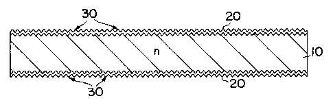
Fig. 1 illustrates a cross-section of a
dendritic web silicon blank of the preferred
embodiment of the invention:
Fig. 2 illustrates the cross-section of
the web at the aluminum deposition stage for the
positive contact;
Fig. 3 illustrates the cross-section of
the web at the heat treatment stage;
Fig. 4A illustrates the cross-section of
the web during the insulation of the first metal
stage to form aluminum oxide:
Fig. 4B illustrates a close-up view of the
back surface portion of the web of Fig. 4A:
Fig. 5A illustrates the cross-section of
the web during the removal of silicon oxide from the
back surface;
Fig. 5B illustrates a close-up view of the
back surface of the web of Fig. 5A:
Fig. 6A illustrates the cross-section of
the web during the deposition of metal for the
negative contact;
Fig. 6B illustrates a close-up view of the
back surface of Fig. 6A;
Fig. 7 is a bottom, back view of the
finished cell;
Fig. 8 is a plan view of the back side
surface of a substrate having 8..cells.; ..- -
Fig. 9 is an enlarged view of the rear
surface of one of the cells on the substrate of Fig.
8;
- Fig. 10 is a sectional view taken along
lines 10-10 of Fig. 9;
Fig. 11 is an enlarged detail view
illustrating a portion of a pair of positive
electrodes and the region therebetween; and
LJPOCL.P50
g PATENT
Fig. 12 is an enlarged detail view
illustrating a corner portion of the top of the Fig.
9 cell.
5 DETAILED DESCRIPTION OF THE PREFERRED EMBODIMENTS
Turning attention now to the figures,
there is disclosed a preferred fabrication technique
and design for the present invention.
While Figs. 1-7 show dendritic web
10 silicon, it is understood that the invention is
meant to apply to any form of silicon, including
float zone silicon, Czocharalski silicon, magnetic
Czocharalski silicon, cast silicon, and sheet
silicon, provided the minority carrier diffusion
15 length under operating cell conditions exceeds the
cell thickness.
The starting material for the back contact
silicon (Si) solar cell of the present invention is
any n-type silicon starting material, shown as layer
20 10. Common n-type dopants for Si include the atoms
from group V of the periodic table, and include such
elements as Li, Sb, P, and As. However, it should
also be understood that the disclosed cell structure
would also function for starting silicon material
25 that is p-type, or even undoped, since layer 10
functions primarily as an absorber of light.
In the preferred embodiment illustrated in -
the figures, the starting material (for the bulk
layer 10 in Fig. 1) is dendritic web silicon doped
30 n-type with antimony (Sb). The dendritic web
silicon ribbon is grown using a process similar to
that used to produce Czochralski (CZ) silicon.
However, silicon grown by other methods may also be
used in addition to dendritic web silicon, such as
35 float zone silicon, CZ silicon, cast silicon, and
IJPOCL.P50
CA 02181281 2004-05-18
9
sheet silicon. The Si dendritic web is typically
grown at a thickness of 100 microns, though other
thicknesses may be used. At this thickness the
minority carrier diffusion length is usually more
5 than the thickness of the cell, often two or three
times the thickness. On both the top and bottom
surfaces of the Sb-doped Si ribbon is placed in a
shallow n+ layer, 20, diffused into both surfaces
while the web is still in the growth furnace. If
10 the n+ surface layers 20 are not introduced during
web growth, they can be incorporated at the
beginning of the process by any proven method known
in the art, including simultaneous front and back
diffusion from a liquid dopant source using rapid
15 thermal processing. The n+ layers create a "surface
field" that drives holes away from the surfaces and
reduces the surface recombination there, as well as
accelerating holes generated in the surface layers
to the p-n junction, and other beneficial effects
20 that work to increase the short-circuit current and
open-circuit voltage to enhance the solar conversion
efficiency. Further, the back n+ layer promotes
ohmic contact to the negative contact metal there,
as described below.
25 In addition, surface texturing of both top
and bottom surfaces is provided in order to trap
more incident light. Such surface texturing,
shown in the form of a saw-tooth pattern 30, may
be grown-in, introduced by anodic etching to create
30 a porous Si layer (as per the method outlined by
Y.S. Tsuo et al., "Potential Applications of
Porous Silicon in Photovoltaics", Conf. Record 23rd
IEEE Photovoltaic Specialists Conf. (Louisville, KY)
1993), or introduced mechanically by sawing
35 or optically such as by laser
2181281
AP TENT
etching. Though in the preferred embodiment
texturing and doped surfaces are shown, their use is
optional in the general case. Further the texturing
of the bottom surface;of the cell is not shown in
5 Figs. 2-6 for clarity.
Figs. 1-6 illustrate important steps in
the fabrication of the solar cell, including the use
of aluminum as both dopant and ohmic contact
material as well as its masking using a self-
10 aligning anodic oxidation technique. Aluminum or
aluminum material herein is defined as either pure
A1 or an A1-Si alloy in which the silicon
concentration is less than eutectic composition
(88.7% A1 and 11.3% Si, by weight). This aluminum
is deposited over approximately half the total back
surface area in stripes spaced edge to edge about
100 ~,m (microns) apart and each 100 ~m wide, as
shown in Fig. 2, at spacing 40. The spacing 40
between stripes 50 should be less than a minority
carrier (hole) diffusion length for efficient
carrier collection. The line width and spacing thus
could be reduced to below 100 ~m to some advantage.
The useful upper limit for line width value is about
2000 um; while the useful range for edge-to-edge
spacing 40 is from about 50 ~m to about 300 ~cm.
Thus the parallel stripes of aluminum each form
separate regions of dopant source material far the
p-n junction solar cell, and, as explained further
herein, are joined (contiguous) at their base to
form a bus bar region for the positive contact bus
bar.
In a preferred method for depositing
aluminum it is deposited by screen printing the
aluminum, a process known per se in the art, in an
aluminum paste. The stripes of aluminum are shown
LJPOCl.P50
11 PATENT
in Fig. 2, where aluminum is deposited, as stripes
50, running into the plane of the paper. However,
methods other than screen printing for depositing
the aluminum are within the scope of the invention,
such as electron beam evaporation or sputtering,
although these methods may require more costly
patterning by photolithography and so are less
desirable.
Generally speaking, the A1 layer of
p-type material is relatively thin when compared to
the n-type bulk layer, about 2 to 20 ~m thick for a
bulk layer with thickness of about 100 um.
Note that in the preferred embodiment of
the present invention the choice of aluminum serves
at least three purposes simultaneously: it acts as
a p-type dopant source, it acts as a positive
contact metal, and it acts as a partial back surface
light reflector over that back surface area it
covers, Which is approximately 50% of the back area.
Turning attention now to Fig. 3, which
illustrates heat treatment, there is shown a figure
depicting the effects of heat treatment of the
deposited Al layer in~an approximately 850°C oxygen-
rich environment. In this step the p-n junction is
formed by alloying the screen-print deposited A1
with the Si. It is further believed that
maintaining a temperature-of 850'-C fnr an extended
period of time, as for example 30-minutes or more,
is beneficial to forming a satisfactory alloy. The
range in temperatures can be from 577°C, the
aluminum-silicon eutectic temperature, to 1420°C,
the melting point of silicon. Heating may be
provided by a rapid thermal processing unit, a belt
furnace, a tube furnace, or other means. The
ambient atmosphere can be inert, such as argon or
LJPOCL.P50
. ~ 2181281
12 AP TENT
nitrogen, or chemically active such as with oxygen
or hydrogen. Mixtures of ambient gases are also
possible. Times at elevated temperatures can range
from 30 seconds to several hours. In the preferred
embodiment it is expected that the use of an oxygen-
rich environment at this temperature will enable
oxide (SiOz) to grow on any exposed Si, which will
passivate the surface and decrease harmful
recombination effects.
The temperature is then lowered in the Si-
A1 alloy, and Si regrows by liquid phase epitaxy
until the eutectic temperature (577°C) is reached.
As a result, the regrown Si is now doped p-type with
A1 (about 10'8 cm 3) , as denoted by the p' layer
composition 60 in Fig. 3. The required p-n junction
is formed as the A1 concentration exceeds the donor
concentration in the starting Si, and the eutectic
alloy (about 88.7% A1 and 11.3% Si, by weight)
remains on the surface to serve as a contact to the
p-type silicon. It should be noted that the p-n
junction may be quite deep (1 to 20 microns from the
surface) but since the junction is at the back of
the cell, where very little light is absorbed, the
junction depth is only of secondary importance as
compared to a conventional front contact solar cell.
The depth of the alloy junction can be controlled by
using an A1-Si mixture as the screen-printed
material deposited instead of pure A1. This is
because as the Si concentration is increased toward
the eutectic composition, the amount of Si that the
printed metal can dissolve becomes less, hence the
junction depth becomes less. The junction depth can
be increased, if desired, by increasing the
thickness of the deposited aluminum and by
LJPOCL.P50
- ~ 2.~8~28~
13 A~ TENT
increasing the alloying temperature, in accordance
with the aluminum-silicon phase diagram.
Further, the bulk lifetime of minority
carriers will probably increase at the approximately
850'C temperature due to the property of dendritic
web silicon (the preferred type of Si used in the
present invention) to have any quenched-in defects,
such as Si vacancies and self-interstitials, anneal
out. Cooling at a controlled rate of 10'C per
l0 minute versus a more rapid cooling will also allow
quenched-in Si defects to anneal out, reducing
harmful recombination sites.
The foregoing heat treatment may be
effected using a belt furnace process in which the
samples are loaded on a belt and the belt is slowly
pulled through stable hot zones in a furnace. In
the alternative to heating the Si/A1 mixture at
850'C for about 30 minutes in such a furnace, one
may employ a variety of other techniques to form the
Si/A1 eutectic, such as the use of a rapid thermal
processing unit that employs by way of example
quartz lamps to heat the Si to 1000'C and maintain
that temperature for 30 seconds, which would
increase throughput in a commercial setting, or by a
conventional quartz tube furnace.
Having such a p~ region (region 60 from
Fig. 3) immediately adjacent to the n'wregion at the
back surface layer (the back surface layer-2~0 from
Fig. 1) also has the unanticipated benefit of
protecting the solar cell from overheating when it
is reverse biased, as for example by shadowing in a
module. A "module" is a group of interconnected
cells which are protected by glass or other cover
material, and which produce a significant amount of
power, typically 10 to 100 watts, when illuminated.
LJPOCL.PSO
2181281
14 PATENT
This p'n' design builds in protection against reverse
bias, eliminating any need to have protection
diodes, commonly referred to as "bypass diodes" to
guard against reverse bias. The p'n' junction acts
5 as a Zener diode which breaks down under modest
reverse biases with only a small voltage and
consequently only a small amount of power is
dissipated in the cell, thus protecting the cell.
Turning attention now to Figs. 4A and 4B,
10 another step in the preferred embodiment of the
present invention is illustrated. This step
provides a unique "self-aligning" feature for
aligning the negative contact (to the n-type region)
with respect to the positive contact (to the p-type
15 region). In order to insulate the p-type layer
contact (positive contact) from the n-type layer
contact (negative contact), the present invention
does not require complicated masking techniques that
have been used in the past, but rather, employs the
20 use of insulation by forming an oxidation layer to
coat the first (positive) set of A1 contacts and
electrically isolate this set from the second
(negative) set of contacts. As shown in Figs. 4A
and 4B, this is done by insulating the
25 A1-Si p' layer composition and the exposed A1 stripes
70 that are on the outside of the web blank 10, with
an oxide layer 80 (insulator);-which forms naturally
on exposed Si, Si-A1 and A1 materials, in the form
of A1203, SiOZ, or some variation thereof, in the
30 presence of oxygen. The oxide layer should be grown
to cover the A1 stripes 70 to a thickness of
approximately 0.1 ~m to 1 Vim. As shown in Figs. 4A
and 4B, at this stage the oxide layer 80 also covers
the n-layer surface regions 90 in between the A1
35 stripes 70. As described more fully below, the
LJPOCL.P50
2I~128~
15 A ENT
oxide layer on the surface regions 90 is
subsequently removed (refer to the step illustrated
in Fig. 5B below) in order to enable ohmic contact
with the cathode (n-type Si) of the solar cell
diode.
The preferred method of forming the
oxidation layer in Figs. 4A and 4B is by anodic
oxidation, in which the layer surface of the
developing cell is immersed in a weak electrolyte
(such as borates, phosphates or carbonates) and
subjected to an applied voltage. Current flows as a
result of a voltage applied between an inert
electrode and the contact metal (the A1-Si
eutectic). The thickness of the anodic oxide can
reach 1 micron if the voltage which drives the
anodization current reaches 700 V (14 A/V or 1.4
nm/V). Such oxides should be compact and free from
pinholes. Because ohmic contact must be made to a
positive contact bus bar (at region 110, shown in
Fig. 7) when the solar cell is finished in order to
make contact with the exposed A1 stripes 70, the
growth of anodic oxide must be inhibited in the bus
bar region (and this bus bar region must be shielded
throughout the process). One way to do this is to
use a compressive yet conductive medium to contact
the area to be occupied by the bus bar, such as a
carbon-impregnated closed-cell sponge. A closed-
cell sponge is preferable as it will not absorb the
electrolyte.
Besides anodic oxidation, any other method
for insulating the aluminum or aluminum-silicon
eutectic layer is also envisioned by the present
invention, such as oxidizing aluminum in an oxygen-
containing plasma.
LJPOCL.P50
2~.8~28I
. 16 PATENT
After the oxidation layer 80 has been
added by anodic oxidation or any other suitable
method, the n-type Si surface covered by the
oxidation layer in interstitial surface regions 90
must be exposed in order to permit the negative
contact metal layer of A1 to be deposited thereon.
Thus, referring to Figs. 5A and 5B, there is
illustrated how the oxidation layer is removed from
the Si layer on the back surface, but not the
oxidation covering the A1 stripes 70. In a
preferred method of doing this, hydrofluoric acid is
used to selectively etch away and remove the
interstitial Si02 (silicon dioxide) 20 because
hydrofluoric acid does not react and remove A1203
(aluminum oxide). Consequently, the interstitial
Sio2 is removed while the A1203 insulative layer
remains covering the stripe contacts 70 (see Fig.
5B). Other chemicals having similar effects may be
used, or other oxide removal techniques may be
employed, such as by light sandblasting of the
silicon dioxide layer, which also provides the
beneficial effect of lightly damaging the exposed
silicon surface, which promotes ohmic contact to the
n-type base. Use of sandblasting eliminates the
need for an n' diffused layer on the back of the
cell, which is usually provided primarily to promote
an ohmic contact. Reactive ion etching (RIE) may
also be used to remove SiOz while leavingA1203
undisturbed. Ion milling may also be used to
lightly damage the surface to promote ohmic contact
in a manner analogous to sandblasting.
Figs. 6A and 6B illustrate the next step
in the process of fabricating the solar cell of the
present invention, viz. the application of a second
metal layer to form the self-aligned negative ohmic
LJPOCL.P50
2~8I28~
17 ATENT
contact metal (for the n-type Si layer contact).
This second metal may be any suitable contact metal,
including aluminum and silver. Again, screen
printing is the preferred method for depositing this
5 second metal, but other methods such as electron
beam evaporation or sputtering are also acceptable.
This second metal layer, designated as metal layer
100, covers nearly the entire back of the cell.
This layer is insulated from the first metal contact
stripes 70 by the anodic oxide 80 while making ohmic
contact to the n' regions 90, found in between the
metal stripes 70 formed from the first aluminum
layer deposited. The second metal layer also helps
form a back surface light reflector to aid in
15 reflecting any light not absorbed by the silicon
material in a first pass back into the silicon
material.
Fig. 7 shows the completed solar cell as
viewed from the back, where the cell is covered with
the second metal (aluminum or other ohmic metal) or
aluminum-silicon eutectic. The solar cell of the
present invention has an unobstructed front surface,
which is a significant advantage over conventional
solar cells. At the back, both metal contacts
(ohmic metal contacts 70 and 100) serve as partial
light reflectors in addition to being ohmic
contacts. Furthermore,-the bus-bar design allows . -.
for the simplified interconnection of solar cells of
the present design in series, as the present design
30 eliminates the need for cumbersome external front-
to-back inter-cell contacts to be manufactured, but
uses more of a "surface-mount" technology design
that dispenses with such contacts.
Thus referring to Fig. 7 there is shown
bus bar region 110, which is the un-oxidized area
LJPOCL.P50
_ . 2.~8~28~
lg PATENT
where the bus bar contact leading to the first
positive contact metal stripes 70 is located, as
explained above. The bus bar region 110 as can be
seen is smaller in area than the area covered by the
negative contact metal, layer 100, but both the
positive and negative metal contacts lend themselves
micely to a modular surface mount design. The
A1-Si eutectic fingers 70 emanate vertically
upwardly from the bus bar 110 of Fig. 7 but are not
visible in the figure due to the overlying second
metal layer 100.
If desired, other ohmic contact metals
than A1 or Ag may be deposited to form the positive
and negative ohmic contacts described herein, such
as by way of example using a titanium/palladium/
copper sandwich or screen-printed silver as
contacts.
Regarding the use of anti-reflective (AR)
coatings, a coating layer or layers would ordinarily
appear on the outermost front illuminated surface,
but they have been omitted from Figs. 1-7 for
clarity. It is possible that an AR coating is
optional with the present design, since texturing,
or perhaps texturing in combination with a
passivating oxide, as explained above, may be
sufficiently effective so as to preclude the need
for an AR coating. However, a~ AR coating such as
silicon nitride applied by plasma-enhanced chemical
vapor deposition (PECVD) or titanium dioxide applied
by atmospheric pressure chemical vapor deposition
(APCVD) can be used. Hydrogen ion implantation (to
improve minority carrier diffusion length) could
also be introduced prior to an AR coating
deposition, provided the surface oxide was absent or
perhaps very thin.
LJPOCL.P50
2~8~~8.I
19 ATENT
REDUCTION TO PRACTICE
With reference to Fig. 8, complete
aluminum alloy junction interdigitated back contact
(IBC) solar cells 120 were fabricated using
Czochralski silicon wafers as starting substrates.
These solar cells serve to demonstrate the use of
aluminum alloy junctions in a back contact
configuration. The aluminum was deposited by
electron beam evaporation, rather than by screen
printing. The negative electrodes were not self-
aligned using anodic oxidation or some other
technique, but rather were manually aligned with
respect to the aluminum-silicon eutectic positive
electrodes with the aid of a contact aligner as used
for fabricating integrated circuits.
The silicon substrate wafers were single-
side polished, 3 inches in diameter, 13-17 mils
thick, phosphorus-doped to 3-20 n-cm, and with a
(111) surface. Two wafers (designated CZ-7 and CZ-
8) were processed with test structures and solar
cells on the polished side. Fig. 8 shows the back
side of one such wafer. The lapped side (hidden
from view in Fig. 8) has a phosphorus diffusion and
an antireflective (AR) coating 95 (see Figs. 10 and
12). Each of the eight solar cells is 1.00 cm
square, ignoring the 2 mm wide bus bar 112 for the
negative electrodes. They are referenced below in
Tables 2 and 3 by the number of n+ fingers forming
the negative contact (4, 8, 16 and 25) and by their
location (interior (I) or peripheral (P)). The four
interior cells have only the eutectic alloy
contacting the p' region, while the peripheral cells
have the second metal also deposited on the
eutectic. Better results were obtained for wafer
LJPOCL.P50
20 PATENT
CZ-8, so only the process and test results for this
wafer will be described.
The process used in fabricating the IBC
cells for wafer CZ-8 is summarized in the table
5 below. A noteworthy feature of this process is that
the back aluminum alloy junction and the phosphorus-
doped n~ layers, formed across the front surface and
at the exposed back surface between aluminum
electrodes, were created in a single high-
10 temperature step. Photolithography was employed to
pattern the evaporated aluminum and to define the
second metal Which serves as the negative electrode.
A back side view of the aluminum alloy junction IBC
solar cell is shown in Fig. 9, while cross-sectional
15 views are shown in Figs. 10-12.
TABLE 1
Process For Wafer CZ-8
Step Description Material Thickness Process
1 Deposit Alumirxan (polished side) Al 3 dun Evaporate
2 0 2 Define pattern (mask 1) AZ 1350) 1.5 Wn Spray, belt
bake
3 Remove alumirxm Al 3 Wn Alumirxm
etch
4 Apply phosphorus liquid dopant P-507 0.3 Wn Paint liquid
25 front and back (over alumirxan> ant
5 Create p regions (alloy) on Al 3 Wn RTP(1000'C,
back and nr regions front and P-507 0.3Wn 30 sec)
beck
b Define pattern (mask 3) AZ 1350) 1.5 Wn Spin, hot
plate bake
7 Deposit wetal (polished side) Ti/Al 500 A/0.5 Wn Evaporate
8 Define contact Na Na Lift-off
9 Protect front diffusion wax undefined Melt using
_ _hot plate
3 5 10 Etch silicon between electrodes n silicon 1.5 Wn 5G:1 NN03:NF,
2 ~nin
11 Apply sntireflective coating Ti02 750 A Spin (2500
rpm, 30 sec)
12 Fire antireflective coating Ti02 750 ~ i50'C, sir
Some comments regarding the CZ-8 process:
Alloy/n+ diffusion process includes a stepped
slow-cool in the rapid thermal processing (RTP) unit
(~50°C/min from 1000°C to 825°C);
LJPOCL.P50
2181281
21 PATENT
There was no apparent harm in painting liquid
phosphorus dopant over the aluminum before the
1000'C RTP process which simultaneously formed the p'
and ri regions;
Depth of p' region detenained to be 5 elm by
cross-sectional scanning electron microscopy for
1000'C, 30 sec RTP process;
Sheet resistance of front n' surface measured
25 iZ/0 after 1000°C, 30 sec RTP diffusion:
Mask 2 was skipped because it was only needed
for some test patterns, not for the IBC cells;
The Ti/A1 contact to n' surface is limited to a
thickness of 0.55 ~,m by the lift-off process;
Without etching n' silicon between positive
electrode (eutectic) and negative electrode (Ti/A1),
the p-n junction was severely shunted.
TABLE 2
Lighted (A111.5, 100 ail/an2, front illunination) I~V Data Before AR Coating
Wafer Cell Jsc V« Fill Factor Efficiency
(~n/an2> (v) <x)
CZ-8 41 22.4 0.516 0.611 ___. 7.07 _._._ ___
C2-8 8I 19.9 0.522 0.621 6.45
C2-8 1bI 19.6 0.518 0.581 5.90
CZ-8 251 20.6 0.510 0.580 6.08
LJPOCL.P50
2181281
22 PATENT
TABLE 3
~i9hted (A111.5,100 ai1/an2, front illunination) I-Y
Data After AR Coating
llafer Cell Jgc Vpc Fill Factor Efficiency
(mA/cm2) (V) (X)
CZ-8 41 27.6 0.515 0.635 9.01
CZ-8 8I 24.2 0.515 0.691 ~ 8.61
CZ-8 16I 23.6 0.510 0.695 8.35
C2-8 25i 23.5 0.505 0.716 8.50
Note that functioning back contact solar
cells wer e obtained, thereby demonstrating the
viability of the disclosed structure. Light-to-
electrica l energy conversion efficiencies up to
9.0%
have been measured. Refinements in substrate
material and processing techniques are expected
to
raise the efficiency to double that demonstrated
to
date.
While the above provides a full and
complete disclosure of the preferred embodiment of
the invention, various modification, alternate
constructions and equivalents may be employed. For
example, while the preferred embodiment has been
described with reference to aluminum for forming the
p-type diffusion and the ohmic contacts, other group
III metals such as gallium and indium may be
employed for this purpose. A suitable group III
element is one which will dissolve the silicon and
remain behind as a trace amount to serve as a dopant
when the silicon solidifies. In addition, while the
LJPOCL.P50
2~S~~SI
23 PATENT
preferred embodiment has been described with
reference to an n-type bulk silicon layer 10,
p-type bulk silicon may be used to fabricate the
back-contact solar cell. When a p-type bulk silicon
layer is used; a thin p; layer is formed on the top
surface as layer 20, but an n' layer is formed on the
bottom of the bulk layer 10. As will be appreciated
by those skilled in the art, in the
p-type embodiment, the minority carriers are
l0 electrons. Therefore, the above description and
illustrations should not be construed as limiting
the scope of the invention, which is defined by the
appended claims.
LJPOCL.P50