Note: Descriptions are shown in the official language in which they were submitted.
~ wogsl24000 2 1 X ~ 6 ~ 2
- 1 .
UUUullUI~ APPARATUS WITH MICROWAVE DETECTIûN
FIELD OF THE IMI'ENTION
The present invention relates to a reproduction apparatus
such as a photocopying apparatus for reproducing documents.
BACKGROUND OF THE INVENTION
The quality of high-resolution color photocopying apparatus
has increased to such an extent that illicit reproduction of
security documents such as banknotes, shares. cheques,
passports, bonds and even credit cards has become easier.
One general solution to the above problem is to provide the
security documents with a marking which can not be copied by
means of a photocopying apparatus. Documents having the
~I~pe~, ~".e of security documents but without the marking can
then be classified as cuu"~, r~iL.
One of the markings provided by the prior art is an optical
marking, since these markings are not completely copied. Wear
and surface damnlage of the genuine security documents may
lead, however, to disappearance of the marking so that
genuine security documents themselves risk to be designated
as counterfeit.
Another marking provided by the prior art is the incorpora-
tion of a thread in the security documents. Examples of
apparatus for detecting the presence of such a thread in
banknotes, and thus for verifying the authenticity of the
banknotes can be found in EP-A-0 092 691 and in
US-A-5.279,403. The material and form of the threads used in
security documents is so diversified. that the design of a
unique apparatus adapted to detect the threads in all secu-
rity documents appears to be impossible. Moreover, these
SUBST!TUTE SHEET ~RllLE 2~)
WO g5124000 P~~ c
2~8~8~ - 2 -
apparatus have as a disadvantage that they can only detect
counterfeit long after it has occurred.
SUMMARY OF THE INVENTION
It is an object of the present invention to avoid the
disadvantages of the prior art.
It is also an object of the present invention to provide for
a system which may prevent falsification of security docu-
ments .
According to the invention there is provided for a reproduc-
tion apparatus, such as a photocopying apparatus, for repro-
ducing documents.
The apparatus comprises a platen for forming a scanning area
and for positioning the documents on its one side.
The apparatus further comprises scanning means for scanning
the scanning area. The scanning means are positioned on the
same or on the other side of the platen. The apparatus also
comprises means for obtaining a relative movement between the
scanning means and the documents in order to allow for the
scanning operation.
The scanning means comprise a microwave system. This micro-
wave system compri ses a number of mi crowave sources for
generating microwaves, a number of microwave emitters for
emitting microwaves to the scanning area. a number of micro-
wave receivers for receiving m~crowaves which are reflected
and a number of microwave detectors for detecting the
reflected microwaves. The number of emitters, the number of
receivers and the number of detectors are greater than or
equal to the number of sources. The number of emitters and
the number of receivers are greater than or equal to the
number of detectors. The position and number of the emitters
and receivers are such that they can detect the presence of
parti cl es havi ng some el e~" _ ~ i c properti es whi ch are
substantial1y different from the ~u.,~uu"ding electromag-
SU3ST!T~TE SHEET ~ E 2~i
` 2~816
O
The presence of the particles ~s detected by their reflecting
at least part of the emitted microwaves back and thereby pro-
ducing a greatly varying reflection signal, whereas in absence
of particles the reflection response signal does not vary to
such an extent.
The above system has the advantage of resulting in a very fast,
almost an instant response, which does nct prolong considerably
the scanning cyclus. Tests have shown that I cm (centimeter~
after having passed over the first present part~cles, a deci-
sion can already be taken about the presence of the particles.
Such a fast speed response can hardly be reached by means of
optlcal systems.
IS Other adYantages of the above system, particularly in compari-
son with optical systems, are that the system is insensitive
for dust, that the presence of any particles can hardly be
hidden by placlng one or another sheet between the sensor and
-the security documents and that a high 1eYel of detectabil~ty
is mainta7ned despite any aging, crumpling or soilage of the
security cocuments.
Microwave systems for detecting the presence of part~cles in a
base mate~ial with substant~ally different el~.L.. ~ -tic
properties are already known in the art (see e.g.
US-A-4,408,15,~; US-A-4,566,121; US-A-4,565,122 and
US-A-4,820,912~, but are not appropriate for the above purpose
of functioning in a reproduction machine and of scanning an
area which is both in length and in width much larger than the
wavelength of the microwaves.
f Within the context of the present invention:
- the terms 'reproduction apparatus' comprise a black and
white copying apparatus, a high resolut~on true Folor photo-
JP-A-~a-c)4~ ~9 d~5c/05es a ca~y~;7g
L ~S ~v~c~ /Oh~- co~7y~`~f o& c~ c~focL~m
ro~vRv~l2 C~ c~7 C~ar~2cc~!rjS~cs of ~C C~oc~ r
,eer ~or~d~e~j"cc~ c~e~.
14l~ENDED SHEET
WO 95/24000 2 ~ ~1 S 8 ~ r~
- 4 -
i
Within the context of the present invention:
- the terms 'r,:,u,udu~ion apparatus' comprise a black and
whi te copyi ng apparatus . a hi gh resol uti on true col or
IJl,uLo~u~ing apparatus, and also a scanning apparatus for
digitizing pictures for further treatment by a computer;
- the term ' pl aten ' i s used for every support structure
transmitting waves and light. where the documents to be
copied can be positioned; it can be flat or cylindrical:
- the terms 'scanning area' refer to the whole area which
can be scanned: it determines the maximum size of the
documents which can be copied in one time:
- the term ' scanni ng ' i ncl udes the so cal l ed pre - scanni ng
for checking the position and dimension of the documents
and the one or more scanning cycli for the copying step
itsel f;
- the terms ' rel ati ve movement ' poi nt to the movement
between the document and the scanning means; two diffe-
rent ~ .lls are possible: a pl~ulu~u~ing apparatus
with a movable platen and a ~I,ulu~u~uying apparatus with a
fixed platen;
- the terms 'microwave source' designate a microwave oscil-
lator which generates microwaves; examples of microwave
sources are a Gunn-diode. a high electron mobility tran-
sistor and a metal semiconductor field effect transistor;
- the terms 'microwave emitter' and 'microwave receiver'
include simple antenna structures such as half wave
dipûles, quarter wave dipoles, microstrip patches and
waveguide apertures;
the terms ' mi crowave detector ' i ncl ude a Schottky di ode
- the terms 'particles having some el~-:l." ,.,~ic proper-
ties which are substantially different from the electro-
magnetic properties of the base material' refer to any
small sized materials which can be i,~o",u, c~d in the
base material of security documents and which have a
dielectric constant ~. a magnetic permeability 1l, or an
; ", . ~ . .
~U~STITUTE SHEET (RULE 26~
O W095124000 21~6~2 P.,l"~, ~ ,
- 5 -
electric resistivity p differing substantially from the ~.
or p of the base material; examples of such particles
are electrically conduc-ting stainless steel fibres being
illculpùlaLed in a base material of paper or plastic:
- the term 'reflecting' also includes scattering back which
does not necessarily occur in the same direction as the
emission of microwaves.
The source, emitter. receiver and detector are not necessa-
rily physically distinct from each other. Following embodi-
ments are possible:
- the function of generating and detecting microwaves is
carried out ~)y one device. a so called self-detecting
diode;
- the function of emitting and receiving microwaves is
carried out bj~ a single antenna or by one simple aperture
in a wave guide:
- the function of receiving and detecting microwaves is
carried out I~y a single detector which receives the
reflected microwaves.
Preferably the microwave system comprises only one source and
a plurality of emitters. receivers and detectors. This
system combines the advantages of being simple and light-
weight and of providing a high signal to noise ratio which is
e.g. higher than 20 dB or higher than 25 dB.
Generally. the means for guiding the microwaves may include
following structures: a hollow wave guide made of metal or
of metallised plastic. planar structures such as microstrips,
striplines and slotlines. and coaxial transmission lines.
For reasons of ful^ther reducing the weight and increasing the
compactness. the means for guiding the microwaves are prefe
rably constituted by the above mentioned planar structures.
SUBSTITUTE SHEET (RU.~ 2~!
WO 95/24000 21~ 1 ~ 8 2
- 6 -
i ~
In this way a microwa~e system can be obtained with a weight
which is less than 100 9. preferably less than 80 9 and most
preferably less than 50 9. It is hereby understood, however,
that such low weights are not excluded if a hollow wave guide
is used.
The copying apparatus according to the present invention may
further comprise means for processing the signal produced by
the reflected microwaves. These processing means can be
digital or analog or a combination of both. The apparatus
also comprises means for generating:
- an 'on' signal in case the presence of particles is
detected in the base material of the documents; and
- an 'off' signal in case the presence of particles is not
detected in the base material of the documents; (or vice
versa) .
In case of the 'on' signal. copying will be prohibited or
only a black copy will be given or another copying resolution
will be used or copying will be done in other colors. and so
counterfeit will be prevented.
In case of the off' signal, the conventional copying process
wi l l proceed .
In a particular t 'il.._.,L of the invention, hereinafter
referred to as third ~ 'il ', the microwave system further
comprises for each emitter a switching diode so arranged that
it can short-circuit the cu,,e~uu,,~ing emitter.
In another: ' 'i,"_.,~ of the invention, hereinafter referred
to as fourth ~ , the emi tters and recei vers are
arranged as resonating structures responding to one single
frequency.
~ithin the context of the present invention, the terms 'reso
nating structure' not only mean structures responding to a
p,~ ""ined frequency range but also structures giving a
SUBSTITUTE SHEET (RULE 26~
O WO95/24000 21~16~2 P~ 8
- 7 -
response as soon as the frequency exceeds a p, ~L~""ined
under limit.
In yet another -'i, IL of the invention hereinafter
referred to as fifth embodiment. each of the emitters
responds to one single resonant frequency which is different
from the resonant: frequency of the emitters. The microwave
system further co~prises means for electronically tuning the
frequency of the generated microwaves so that by generating
microwaves with changing frequency each emitter becomes
sequentially active.
In still another b~ L of the invention hereinafter
referred to as si~th il _ lL the array of emitters loads
a resonating structure like a cavity resonator.
In a seventh IL, the microwave system comprises two
transmission systems. one transmission system for transmit-
ting the generated microwaves and reflected microwaves in one
Z0 polarization. and another transmission system which is
decoupled from t~le first transmission system and which is
adapted for L-~"~",ilLirg reflected microwaves in a polariza-
tion system which is different from or equal to the polariza-
tion system of the generated microwaves.
Finally, in an eighth embodiment one microwave source and a
plurality and equdl number of emitters. receivers and detec-
tors is used. The detectors are positioned close to each
emi tter .
BRIEF DES~RIPTION OF THE DRAWINGS
The invention will now be explained into more detail with
reference to the accompanying drawings wherein
FIGURE 1 gives an upper view of banknotes lying on a glass
platen of a copying apparatus;
SUBSTITUTE SHEET (P,ULE 2~)
WO95/24000 2 1 8 ~ ~ 82 . ~
- 8 -
FIGURE 2 giYeSi 'à cross-sectional view of the relevant
parts of a copying apparatus:
FIGURE 3(a) illustrates an embodiment of a microwave
system using directional couplers:
FIGURE 3(b) gives a schematic r~,u, c:ae:"LdLion of the micro-
wave system illustrated in FIGURE 3(b):
FIGURE 4(a) illustrates an embodiment of a microwave
system usi ng swi tchi ng di odes
FIGURE 4(b) gives a schematic representation of the micro-
wave system illustrated in FIGURE 4(a):
FIGURE 4(c) gives a schematic ,~ "LGLion of the cross-
section of a microstrip alternative of the microwave system
illustrated in FIGURE 4(a):
FIGURE 5(a) illustrates a microwave system making use of
resonant slots:
FIGURE 5(b) gives a cross-section of the microwave system
of FIGURE 5(a) according to the line V V.
FIGURE 6(a) gives a schematic l~ s~llLaLion of a conven-
tional slot in a waveguide:
FIGURE 6(b) and FIGURE 6(c) give schematic ~ s~"LdLions
of slots where use can be made of the technique of depolari-
zati on .
FIGUREs 7(a) and 7(b) illustrate a single-source multi-
detector system.
DESCRIPTION OF PREFERRED EMBODIMENTS OF THE INVENTION
The idea behind the present invention is based on the
following principle: instead of developing systems for
detecting possible counterfeit documents long after the
actual counterfeit has occurred and thus long after the
counterfeiting bird is flown. the present system aims at
preventing counterfeit, or at least at making it counter-
feiters more difficult at the time they try to counterfeit.
The present invention provides for a system which prevents a
certain class of documents. hereinafter called 'security
SU35TITUTE SHECT ,,;ULE 26)
~ WO 9S124000 ~ 1 ~ 16 ~ ~ r~
. g
documents' to be copied. e.$. by means of a highresolution
color copying apparatus. The terms 'security documents' cover
all documents such as banknotes. shares, cheques. passports,
bonds and even credit cards or the lil~e, having a base mate-
rial with ele~L,~ Lic properties some of which differ
sensibly from the cu" ~,uu"ding ele~L~, ,.I~Lic properties of
any parti cl es to be i llcu, ,uùl c Led i n the base materi al, e . 9 .
a base materi al s~hi ch i s substanti al 1 y el ectri cal 1 y non -
conductive. Examples of such base material are paper and
pl asti c .
In order to prevent the copying of the security documents.
these documents should contain in at least a part a number of
particles such as stainless steel fibres. For reasons of
simple mix with the base material and for other reasons which
will become clear hereunder. the stainless steel fibres are
preferably spread over the complete document.
Usually the documents comprise less than 5 % by weight of
stainless steel fibres. e.g. less than 1% by weight or less
than 0.5 X by weigllt. The stainless steel fibres are randomly
distributed in the documents.
The stainless steel fibres have a length which is smaller
than 40 mm. preferably smaller than 20 mm. and most prefe-
rably smaller than 10 mm. e.g. 3 à 6 mm.
The reason of the limitation of the length is to allow an
easy mix with the base material and to avoid a considerable
influence of the stainless steel fibres on the visual aspects
of the documents.
The stainless steel fibres function as an electrical dipole.
They can even give a resonant reflection. The fibres have,
despite a low cu,,Lt:,,L,~Lion and even with low microwave den-
sities, a relatively high reflection rate. This means that
the consumed mi crowave energy can be kept very smal l, a
source power of e.g. about 5 mW is sufficient, which means
that an additional electrical load is not put upon the
reproduction apparatus.
Sl !~ST~TU~E SHEET (RULE
WO 95/24000 2 18 1 6 8 2
- 10 -
~,. I '.`, .
I . . . ! d`. ,
The microwave radiation level caused by the present microwave
system is very limited. which means that no potential health
risks are associated with the system.
The stainless steel fibres have a d~ameter which is smaller
than 50 micrometer and which is preferably in the range of 2
to 25 micrometer, also for reasons of visual aspects of the
documents.
The presence or absence of the stainless steel fibres will be
detected by means of a microwave system. Micro~ave frequen
cies may range from 1 to 50 GHz (GigaHertz), but the length
and the diameter of the stainless steel fibres determines the
optimal frequency.
For stainless steel fibres having a length between 2.5 and
10 mm. e.g. about 6 mm, a proper frequency range is between
20 and 30 GHz, e.g. about 25 GHz.
With respect to the diameter of the stainless steel fibres an
optimal frequency is obtained if the penetration depth of the
microwaves as a consequence of the skin effect is equal to
half the diameter.
Due to the high frequencies between 20 and 30 GHz, very fast
detector responses are possible.
FIGURE 1 illustrates a platen glass 10 of a photocopying
apparatus forming the scanning area. The thickness of such a
platen glass 10 usually ranges from 2 to 6 mm, e.g. from 3 to
5 mm. Documents such as banknotes 12 lie on the platen glass
10 and comprise stainless steel fibres 13 randomly distri-
buted over the whole volume of the banknotes 12.
Assume, for example, that the surface of the scanning area i5
equal to the surface of a standard DIN A4 paper, which is
21 cm x 29.7 cm, and that the width of a banknote is 7 cm.
The maximum detection width obtainable with a single emitter
and receiver in the frequency range of 20 to 30 GHz is about
1 cm to 1.5 cm. It is not possible to detect with one single
linear scanning movement the presence of banknotes having
SUBSTITUTE SHEET (;'.~'LE 26)
O W09!;124000 2~81~g2 P.l/~. f~
- 11 -
stainless steel fibres ill.ul yul ~L~d therein, since proper
positioning of the banknote. e.g. in the longitudinal direc
tion and somewhat remote from mthe course of the emitter and
receiver could a~/oid detection. Taken the above example of
the A4 scanni ng area and assumi ng that the banknote has
stainless steel fibres spread over its whole volume and
assuming that the scanning movement is done in the longitu-
dinal direction of the A4 scanning area, four sensors would
be sufficient to detect all possible positions of a banknote.
Security documenl;s having smaller linear dimensions (e.g.
credit cards), or security documents having only in a part of
it stainless steel fibres in~u, ~,u, ~Led. or a scanning area
being larger than a DIN A4 document would require more
sensors .
FIGURE 2 illustrates in cross-section the parts of a photo-
copying apparatus 14 which are relevant for the present
invention. The photocopying apparatus 14 comprises a platen
glass 10 whereupon the documents 12 to be copied are posi-
tioned. A cover 16, e.g. an auto document feeder (ADF) cover
may be provided above the platen glass 10. Scanning means 18
are provided under the platen glass 10 and perform one or
more scanning movements immediately before and during the
copying process.
Scanning speeds in direction of arrow 20 usually range from
100 to 300 mm/s. e.g. from 150 to 250 mm/s. The detection of
the presence of stainless steel fibres in security documents
should be preferably done at the same scanning speeds, thus
without decreasing the scanning speed.
The return speeds of the scanning means 18 in the direction
of arrow 22 are mllch higher, and are up to 1000 mm/s and even
to 1600 mm/s and more. So the additional microwave system for
the detection of stainless steel fibres should add as little
as possible weight to the scanning means. The total weight of
SUBSTilUTE SHEET (RULE 56)
WO 95/24000 2 1 8 1 ~ 8 2 . ~ " ~ ~
- 12 -
~ .
, . . ~ ~ .
the scanning means 18 with inclusion of a microwave system
should be preferably limited in the range of 400 to 600 g.
First ~
A first microwave system for detecting the presence of stain-
less steel fibres in documents on the scanning area can be
embodied as follows: an array of e.g. four il~d~ wor-
king transceivers. Each transceiver has a Gunn diode working
as a microwave source, a sensor head which includes the
function of emitter and receiYer and which substantially
functions as an open-ended waveguide for the transceiver, and
a detector diode, such as a Shottky diode or a point contact
diode, providing a very fast DC voltage response. The trans-
ceivers are divided over the width of the scanning area. The
output signals of the four detector diodes can be connected
in an OR circuit which produces an 'on' signal in case at
least one of the transceivers detect the presence of stain-
less steel fibres.
This first system has, however, the drawback that four Gunn
di odes are needed, whi ch i ncreases the cost and al so the
weight of the microwave system.
Second ~
In order to reduce the cost and the weight of the microwave
system a second microwave system may be designed where only
one transceiver is used for an array of, for example, four
sensors heads. FIGllRES 3(a~ and 3(b) illustrate such a
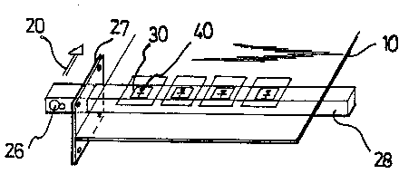
microwave system 24. One transceiver 26 is connected by means
of bolts and a flange 27 to a waveguide 28 with four sensor
heads 30. Directional couplers 32, e.g. hybrid 3 dB couplers,
positioned at the small sides of the waveguide are used to
divide the power over the sensor heads. The transceiver 26 is
basically constituted by a Gunn diode 34, a circulator 36 and
a detector diode 38.
SllBSTiTUTE SHEET (RULE 26)
2186~
~ W095124000 = = r~
- 13 -
A flange 27 is not necessary. In order to reduce the volume
and the weight of the microwave system it can be omitted and
the wave guide 28 can be directly welded on the transceiver
26.
5 Although having ~s advantage that only one Gunn diode and
only one detector diode is used, this second microwave system
has a number of drawbacks.
A first drawback is that due to the division of the available
power and due to losses in the directional couplers as a
col,s~y~ e of the use of high frequencies, only a fraction
of the generated l~ower is available at the sensor heads, and,
consequently, only a fraction of a fraction of the generated
power can be reflected by the stainless steel fibres and
become available at the detector diode. This may lead to the
necessity of more powerful and thus more expensive Gunn
diodes, to other decision algorithms in the signal processing
or to more complex electronics.
A second drawback is that, if a waveguide structure is used
to transmit the microwaves, the use of directional couplers
can lead to a ratller complex construction as shown in FIGURE
3(a), which requil~es expensive machining or casting and which
is no longer very compact and not light weight. This drawback
may be solved b~ using e.g. microstrips as transmission
medi a .
Third . ~
A third microwave system which has a design which is straight
forward and which provides a solution to the problem of the
power division of the second microwave system, has been
illustrated in FIGUREs 4(a), 4~b) and 4(c).
Referring to FIGUREs 4(a) and 4(b), the sensor heads 30, if
of a proper dimension, function together with the waveguide
28 as an open ended transmission line. Switching diodes or
PIN diodes 40. which are known as such in the art. are posi-
tioned at each sensor head 30 and can be used to short
SUBSTITUTE SHEET (RULE 26~
. .
W095124000 2 1 ~ 1 ~ 8 2 P~
- 14-
circuit all but one of the sensor head 30. so that the entire
power generated by the transceiver 26 i5 available at the one
sensor head which is still open. The switching diodes 40 can
be switched on and off periodically or sequentially so that
each of the four sensor heads 30 is connected somewhat less
than 25 X of the time, taking into account a small dead time
for each switching. The switching can be done synchroneously
with the clock frequency of a mi~ O~ . e.g. at 25 MHz.
If a waveguide structure 28 is used, the sensor heads can be
l ocated i n the smal l wal l of the wavegui de . A very l i ght
wave-guide with dimensions of about 10 mm by 5 mm and made of
aluminium is very suitable for the building in a photocopying
appa ratus.
FIGURE 4(c) schematically illustrates a transversal cross
section of a microstrip alternative. The microstrip is basi
cally constituted by a central conductor strip 44 which is
pl aced between two di el ectri c l ayers 48, 50 and two outer
conductors 42 and 46. Suitable sensor heads or windows 30 can
be made in one outer conductor 42 and a switching diode 40
can be placed across this sensor head 30. Having regard to
the high frequencies used. teflon or similar material can be
used for the dielectric layers 48. 50 in order to reduce the
dielectric losses. Microstrips have the advantage of allowing
cheap mass production and of providing a microwave system
which can be easily integrated in existing copying apparatus.
When using microstrips. a waveguide transition for the
transducer is necessary or a more expensive transducer in
microstr~p must be used.
Fourth ~
A fourth microwave system has been depicted on FIGUREs 5(a)
and 5(b). It makes use of the so called technique of resona
ting structures which take in case of a waveguide the form of
S~BSTITUTE SHEET (RULE 26~
o wo ssn40oo 2181~; 8 ~ r~
- 15 -
resonant slots. This technique is known as such in the field
of radar antennas for transmission over large distances.
The resonant slots are formed by the sensor heads 30 on the
broad side of the waveguide 28 in a metal strip 52 with a
5 width of about 20 mm which is connected to the waveguide 28.
Proper design and positioning of the slots 30 over the width
of the wavegui de wi l l di vi de the generated power equal l y over
the four slots 30i. 30ii. 30111 and 30~V. The length of each
slot 30 is about llalf a wavelength. The slot 30i which is
positioned nearest to the transceiver 26 is positioned away
from the center lille 54 in order to avoid that all generated
microwave power ~ould disappear through this slot 30i.
Correct positioning of the first slot 30i away from the
center line makes that 25 X of the generated microwave power
is available at this first slot 301 and that 75 X of the
generated microwave power passes the slot 30i. In order to
make also 25 % of the generated microwave power available at
the second slot 30ii, this second slot 30ii is positioned
somewhat nearer tc the center line 54 than the first slot
301, since only 75 % of the generated power is available.
50 X of the generated microwave power passes the second slot
30ii and in order to make also 25 X of the generated microwave
- power available at the third slot 30111, this third slot 301i'
is positioned still somewhat nearer to the center line 54
than the second slot 30ii. since here only 50 % of the gene-
rated power is available. Only 25 % of the generated micro-
wave power passes the third slot 30iii, which makes that the
fourth slot 30iV should be positioned on the center line 54
in order to make this remaining power available at the fourth
sl ot .
Correct positioning of the four slots 30 over the length of
the wave guide 28 avoids that the power reflected through one
slot does not disappear through the other slots but is trans-
mitted until the transceiver 26.
SUBSTITUTE SHEET (RULE 26~
WO 95/~4000 2 181~; ~ 2 r~
- 16-
. ~
The dimensions of the,w,aveguide 28 are very limited for the
applied frequency range (about 10 mm x about 5 mm), as a
consequence a very small, compact and light structure can be
obtai ned .
In case the waveguide 28 of FIGURES 5(a) and 5(b) is replaced
by a stripline or microstrip, the resonating structures can
be formed by so-called patch antennas placed on a dielectri-
cum of the microstrip or stripline. These patch antennas are
formed by small electrically conducting plates.
A number of alternative configurations are possible with this
fourth system.
If the number of sensor heads increases, a slotted waveguide
can be used both ends of which can be connected to a trans-
cei ver . Each transcei ver can then feed onl y part of the
number of sensor heads.
The technique of the resonant slots can also be combined with
the technique of the switching diodes in order to avoid the
problems connected with the division of power.
.
Fifth e.. Ju~
In a fifth microwave system use can be made of transceivers
which have means such as a varactor for electronically tuning
the frequency in function of a determined input voltage. Such
varactors are currently available on the market. For example,
the frequency can change from 24 GHz to 25.5 GHz for a
voltage change of 3 V (volt), A first resonant slot in the
waveguide can be designed to respond to a frequency of 24 GHz
(0 V), a second slot to 24.5 GHz (1 V), a third slot to 25
GHz (2 V) and a fourth slot to 25.5 GHz (3 V). In this way
each sensor is sequentially active during the time its
frequency is generated and full reflected power is available
during this time. This technique is often called frequency
mul ti pl exi ng .
SUBSTITUTE SHEET (RU~E 2~3
O WO 95/24~00 2 18 ~ ~ 8 2 r~
- 17 -
Sixth embodiment.
According to a sixth microwave system, the array of sensor
heads can be des~gned in a way that the array loads a
resonating structure such as a cavity resonator. The trans-
ceiver feeds its power into the cavity via a coupling device
such as an iris. The power gets lost in the cavity and
through the sensor heads. The presence of a stainless steel
fibre passing in the detection field of one of the sensor
heads will detune the cavity resonator, which can be easily
observed by the detector diode since all power becomes
available for the detector diode. This sixth system has the
advantage of requiring only simple electronics, of working
with only one frequency, of possible provision of a light-
weight system and of a possible presence of a lot of sensor
heads.
The difference with the fourth system is that in the fourth
system each slot functions as a resonating structure on its
own while in this sixth system the waveguide as a whole with
inclusion of all its slots functions as a resonating
structure.
Seventh embodiment.
In yet another and seventh microwave system use can be made
of the technique of depolarizations. Referring to FIGURE
6(a), the generated electric field Eg has always its orien
tation parallel t~) the small side of the sensor head 30, a
stainless steel fibre will, supposing its orientation in the
security documents is at random, not only reflect an electric
field E,1 component which is parallel to the generated elec-
tric field Eg but also reflect an electric field E,2 component
which is perpendicular to the generated electric field Eg. If
no measures are taken, the electric field component E,2 iS
lost for detection purposes.
The sensor windows 30 can now be designed in such a way that
the reflected field component E,2 is also received for
SUBST~r.lTE SHEET (RULE 2~)
.
WO 95124~00 2181 Çi ~ e ( 9
- 18 -
detection purposes. FIGUREs 6~b) and 6(c) show two possible
"e:llLs of such a sensor head 30.
The electric field component E,l can now be collected in the
same transmission system as the one for the generated elec-
tric field Eg and the electrical field component Er2 can be
collected in another transmission system which is decoupled
and which is adapted for another polarization system. This
depolarization technique, which is known as such in radar
applications, may allow for higher powers available at the
detector diode.
Eiqhth ~ ' ' il,.~,ll . _
FIGURE 7 ( a ) i l l ustrates an ei ghth ' ' i ,..~., L whi ch i s a
si ngl e - source mul ti - detector system . A si ngl e source 26,
e.g. a Gunn-diode, generates microwaves which are transmitted
in the waveguide 28 to four sensor heads 30 which take the
form of slotted apertures in one of the sides of the wave-
guide 28. Preferably, each of the sensor heads is positioned
from the source 28 at an integer number of times half the
wavelength of the waves in the guide in order to optimize the
available energy at the sensor heads 30. The end of the wave
guide 55 is positioned from the nearest sensor head 30 at an
uneven and integer number of times a quarter of the wave
length of the waves in the guide in order to maximize the
available standing wave in the waveguide. A detector module
56 is positioned close to each sensor head 30. This detector
module 56 is a small printed circuit board which is fixed to
the waveguide 28. FIGURE 7(b) shows a more detailed and
enlarged view of such a detector module 56. Its real dimen-
sions can be about 8 mm x 30 mm. Reflected microwaves are
received at antenna 58. The voltage signal of these reflec-
ted microwaves is amplified by the printed circuit and is
available as an output signal between connection points 60
and 62. The detector module 56 is fed by a direct voltage of
5 V at point 64. The output signals provided by the four
Sl.IBSTITUTE SHE~T (RULE 26)
~ ~181~82
- 1 9
Moreover, s~ainltss steel fibres, and specifically stainless
stee~ fibres, ~lave in the context of this invention a very
small concentration in the base material, e.g. smaller than 5 %
by weight, and l~referably smaller than 0.5 9~ by weight. Due to
this small concentration and due to the high reflection rate,
the microwaves almost detect the individual fibre within the
base material"dhich means that a response signal with a wide
varying range can be obtained which allows to differentiate
from ambient influences.
This wide varying signal can lead to very simp~e decislon
algorithms which can be based on calculating the standard
deviation or the variance of the microwave reflection over at
least a part of the document. Such a decision algorithm is
robust in a sense that it can be applied in different copying
appara~y,s, e.g. copying apparatus with different kinds of
covers .
In case the calculated value of the algorithm exceeds a criti-
cal level, the presence of individual fibres in the document is
detected and an 'on' signal can be produced. In case the calcu-
lated value rem~ins below a critical level, no invidual fibres
are detected and an 'off' signal is produced.
In spite of the above-mentioned particular idvantageous charac-
teristics of the individual stainless steel fibres, particular
Z5 care must be taken to the cover of the photocopying machine
which may contain an inner reflecting surface which is often
made of electrically conducting material and to the metallic
parts of an ADF cover.
A solution to the first problem of the inner surface of the
cover is found by using an inner surface which is light reflec-
ting but which is of such a small degree of electrical conduc-
tivity that microwaves are not substantially reflected. The
inner surface of the cover facing the platen 10 can be formed
by e.g. a very thin sputtered metallic foil, a foil covered
AMENDE0 SI~EET
W0 95124000 2 18 16 ~ 2 r~ "0
- 20 -
.~:
robust in a sense that it~cin be applied in different copying
apparatus, e.g. copying apparatus with different kinds of
covers .
In case the calculated value of the algorithm exceeds a
critical level, the presence of individual fibres in the
document is detected and an 'on' signal can be produced. In
case the calculated value remains below a critical level. no
invidual fibres are detected and an 'off' signal is produced.
In spite of the ~LO~ i lioned particular advantageous
~l,d~a~, istics of the individual stainless steel fibres,
particular care must be taken to the cover of the photo-
copying machine which may contain an inner reflecting surface
which is often made of electrically conducting material and
to the metallic parts of an ADF cover.
A solution to the first problem of the inner surface of the
cover is found by using an inner surface which is light
reflecting but which is of such a small degree of electrical
conductivity that microwaves are not substantially reflected.
The inner surface of the cover facing the platen 10 can be
formed by e.g. a very thin sputtered metallic foil, a foil
covered with an aluminium coating applied by chemical vapour
deposition, a metallic lacquer or a metal sheet covered on
its free underside with a dielectric ~ ~"~I,a, ~lll, layer.
Another sol uti on i s to use a mi crowave absorbi ng i nner
surface, e.g. by carefully positioning at least two conduc-
tive layers parallel to one another.
Yet another solution to the first problem can be explained as
follows. It is possible to tune the microwave system in such
a way that the sensor heads or sensor wi ndows recei ve a
maximum response signal for any present stainless steel fibre
while any electrically conductive plate such as a metal plate
does not give a response signal by reason of its proper posi
tioning with respect to the sensor heads or sensor windows:
Sl)BSTITUTE SHEET ~RULE 26)
o wo ssl24000 ~ 1 8 1 ~ ~ 2
- Z1 -
the tuning can be such that a maximum response is obtained at
any distance which is an uneven multiple of a quarter wave-
length, this is the proper place to position the security
documents: at any even multiple of a quarter wavelength a
minimum response is obtained, this is the place to position
any present, electrically conductive plate.
A possible solution to the second problem of the ADF cover is
found to il~C~ al,~ into the belt of such an ADF cover a
metal 1 i c foi 1 or a foi 1 covered wi th an al umi ni um coati ng
applied by chemical vapour deposition, or a metallic lacquer
in order to shield against any ambient reflections.
The above problems of the inner reflecting surface and of the
ADF cover can also be overcome by the use of more complex
decision algorithI~s which can be implemented in hardware or
in software or in a combination of both. Generally, these
decision algorithlns may include following modules:
- a module which differentiate between a fibre and a metal
plate: if the continuous and constant presence of an
electrically conductive material is detected over a prede-
termined distaIlce, this material is identified as a metal
plate and not dS fibres:
- a module which determines the size of electrically conduc-
tive materials; if this size is much smaller than the
Z5 size of that p~rt of the documents which are expected to
comprise fibres, the material is not identified as fibres
but as e . g . a metal stapl e used to hol di ng documents
together;
- a module ~hich detects fibres and which comprises a band-
pass filter to filter out the frequency range of a typical
response generated by the fibres.
SIJ~STITUTE SHEET (RULE 26)