Note: Descriptions are shown in the official language in which they were submitted.
~ wo g~,2,383 2 1 8 1 9 9 3 PCT~~ 330
METHOD OF MAE~:rNG A MIORt~M13rH~NICAL
SILICON-ON-GLA~S TUNING FORK GYROSCOPE
FIELD OF THB lr v~
This invention relates in general t.o a method of making
a mi.;.- - -nic~l device, and in particu].ar to a method of
making a mi~;L. ~ niCAl sili~ ,.. glass tuning fork
l ly L :)scu~.e .
p~ r r OF THE lh~
There are many methc~ds of performing the functions of
a yyLc,s~ .e: rotating di-~c, rotating sphere, quartz tuning
1~ fork, fiber optic laser, h~micrh~rical r~cnnAnf-e~ etc. In
addition there are a number of known mi.:L. - =n;cal
~yL~,scu~e implementations, such as gimbal~.ed yyL~.s.:ul-e:" and
polysilicon and metal tuning fork yyL~scopes.
The "bulk" or non-mi~:L- --hAnical gyroscopes are much
larger, heavier, and expensive. Previous mi~:L- - Anical
gyroscopes have low sensitivity, are difficult to fabricate
due to multiple masking and prsc~cc; n~ steps, and have
problems with movable ]llasses coming into contact with
electrode material and st icking .
Sticking occurs when a resonating mass comes into
contact with an underlying metal electrode, typically gold,
and fails to spring free, ultimately ending in device
failure. The magnitude of drive forces and ~ S~ULe:S that
can be applied to a gyroscope prone to sticking is
necF~cc~rily limited by this phF~n~ 1.
8UMNhRY OF THE lh V ~ ~ . lU rl
According to the teaching of the present invention there
is provided a method for fabricating a mi.:l, ^hAnical tuning
fork gyroscope which includes single sided processing of a
silicon substrates and a glass substrate, anodic bonding of
the resultant substrate structures, and a f inal etch step to
free the tuning fork elements. The method requires fewer and
_ _ _ _ _ .. _ _ _ _ _ _ _ _ _ _ _ . _ . .. .
~!0'151213~'3 ' ' 2 1 8 1 9q3 PCT~-~9510133~1 ~
-- 2 --
simpler processing steps, thus resulting in a lower cost and
easier to fabricate mi~:L, ~n~cal gyroscope.
In particular, the method is defined herein with respect
to a comb drive mi-;L~ -^h~n;rs~l tuning fork yyLuscu~e. Such
a yyLosuuue has a first surface of a glass substrate over
which is s~1~p~n~d a silicon rotatable assembly comprising
f irst and second vibrating assemblies extending from one or
more anchors. Disposed at either end of the respective
vibrating assemblies are drive and driven finger electrodes
formed by plural respective interleaved fingers for imparting
vlbrational motion to the tuning fork vibrating elements.
The finger electrodes greatly increase the area and
capacitance as well as the capacitance change with motion of
the device so as to substantially enhance system sensitivity.
The method of fabricating such a gyrûscope takes place
on a first surface each of a silicon substrate and a glass
substrate. With regard to the silicon substrate, one or more
recesses are formed using potassium hydroxide (KOH). A
single subsequent boron diffusion def ines the thickness of
the silicon yyLuS~:u~: structure. Finally, the features of
the structure are def ined by using a reactive ion etch (RIE)
beyond the boron etch stop layer in selected locations.
The glass substrate processing involves a first step of
selectively recessing the first surface of the glass. Next,
a multi-metal system such as titanium-platinum-gold is
deposited on the recessed first surface, then selectively
lifted off, leaving a planar glass surface with metal
deposits only slightly extending beyond the surface.
Finally, one substrate is inverted over the first
surface of the other, the two are aligned, and are then
anodically bonded. Lead transfer to the silicon is achieved
through contiguous gold deposits; due to the high temperature
at which the binding process occurs, the silicon and gold
sinter, thus forming a chemical bond.
While the low profile, recessed metal deposits as
described may provide sufficient reduction in the potential
Wo 9S~213~3 2 1 8 1 9 q 3 Pcrr~lsg~0133o
-- 3
for portions of the silicon gyroscope structure to impact a
portion of the multi-metal systems, such impact would likely
occur in gyr~-~ opes subject to extreme angular rates and/or
physical sho~ . Sticking between the silicon and the
' 5 uppermost gold layer would then result, partially due to gold
being a soft material. By removing the gold in an alternate
PnhOr~i L, the exposed surface of the multi-metal system is
the hard platinum layer.
The step of removing the gold from metal deposits
subject to silicon imp,~ct increases the resistance to
sticking. However, a further step can be taken to
signif icantly decrease the likelihood o~ this device failure
mode. Specifically, the platinum layer can be patterned to
form an array of stand-ofs or posts which reduce the contact
area where the masses iml~act. Since the sticking tendency
is a function of surface area in contact, sticking is
n~c~cc~rily reduced by th~ formation of these platinum stand-
offs.
The tuning fork ~yroscope ~ho~ thus formed
provides reduced discret~- processing steps with a resultant
reduction in production cost and fabrication time, and
~nh;~nr -~r1 resistance to adhesion between the silicon
:~LLU~;LI~L~ the glass sub~trate and the metallic electrodes
rl; ~:p~>sed therebetween . Another benef icial result of the use
of the method disclosed herein includes reduced parasitic
capacitance from the use of a glass substrate.
BRIEF D~ A~.~.10N OF q~HE DRAWING~
These and other fea~ures of the present invention are
more fully set forth below in the fully exemplary detailed
descr iption and ~ n~ring drawing of which:
Fig. l is a plan diagrammatic view of one embodiment of
a mi~:L, -~h~n;ral comb drive tuning fork yylOSCu~t:
manufactured according to the method of the present
invention;
WO ~121383 2 1 8 1 q 9 3 PCT111S~ 1331~ --
-- 4 --
Fig. 2A is a partial section view of a silicon substrate
illustrating a step of the method of the present invention;
Fig. 2B is a view of the substrate of Fig. 2A
illustrating a further step in the method of the present
invention;
Fig. 2C is a view of the substrate of Fig. 2B
illustrating a further step in the method of the present
invention;
Fig. 3A is a partial section view of a glass substrate
illustrating a step of the method of the present invention;
Fig. 3B is a view of the substrate of Fig. 3A
illustrating a further step in the method of the present
invention;
Fig. 3C is a view of the substrate of Fig. 3B
illustrating a further step in the method of the present
invention;
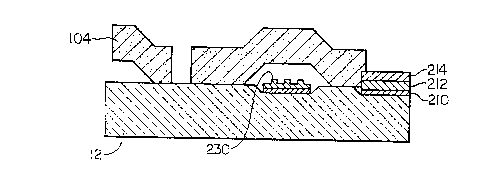
Fig. 4A is a partial section view of the substrate of
Fig. 3C disposed over the substrate of Fig. 2C according to
the method of the present invention; and
Fig. 4B is a view of the substrates of Fig. 4A
illustrating a further step in the method of the present
invention .
DE:TDTT.Rn l;iB~r_nl~l OF TIIF l~VLn~_
The present invention contemplates a mi. L -n j cal
tuning fork gyroscope 10 fabricated by a dissolved silicon
wafer process whereby electrostatic bonding forms a hermetic
seal between an etched glass substrate 12, metal electrodes
deposited thereon, and a silicon comb drive tuning fork
gyroscope 14. The dissolved silicon wafer process involves
single sided processing of a silicon substrate, including the
steps of etching recesses, diffusing an etch resistant dopant
into the silicon substrate, and releasing various components
of the silicon gyroscope by etching through the diffusion
layer in desired locations. The glass substrate also
undergoes single sided processing, including the steps of
Wo 9S/~1383 2 1 8 1 9 q 3 PcrIUS~S/01330
etching recesses, depositing a multi-metal system in the
recesses, and selectively etching portions of the multi-metal
system. One substrate is inverted over the other and aligned
before anodic bonding of the two substrates is performed.
In Fig. 1, one ~ ~~ L of a comb drive llyLUSCu-u~ 14
fabric~sted according to t~le present invention is illustrated.
The gyroscope thus formed employs drive 16 and driven finger
ele.;LLudes 18 formed by plural respective interleaved fingers
24 for imparting vibrational motion to the tuning fork
vibrating elements 20 . The f inger electrodes greatly
increase the area and capacitance as we~l as the capacitance
change with motion of the device so as to substantially
enhance system sensitivity. Moreover, such an electrode
structure is compatible with the dissolved silicon wafer
process d i Cclos~d herein . The tuning fork gyroscope 14 thus
provides reduced parasiti~ capacitance resulting from the use
of a glass substrate, reduced discrete processing steps with
a resultant reduction in production cost and fabrication
time, and ~nh;ln~d resist;mce to adhesion between the silicon
structure, the glass substrate and the metallic electrodes
d i erosed therebetween .
It is understood that the process as described herein
is applicable to the fabrication of various: .~i- Ls of
mi~:L - -n i ~al comb-drive gyroscopes other than that shown
in Fig. 1. However, common features of these gyroscopes
include the following el~ments. A first surface of a glass
substrate has sllcp~nd~d thereover a silicon rotatable
assembly 30 comprising first and second vibrating assemblies
20 which extend from one or more anchors 32. The vibrating
assemb~ ies 20 are comprised of opposing comb :.~LuuLuLes made
up of driven electrode fingers 24 extending therefrom.
Disposed on the first surface of the glass substrate are
cooperating drive elect:rode f ingers 16 for alternating
alignment with the drive~!l finger electrodes 18. Torque 36,
or rebalance, and sense electrodes 38 are dicpoc~-1 on the
glass substrate beneath a portion of the vibrating assemblies
Wo ~S/21383 2 1 8 1 9 9 3 PCT/U~g~/0l331~ --
-- 6 --
and/or support structures extending between the vibrating
assemblies and the anchors . Also r7. i cpocPd on the glass
substrate are metallic conductive leads 40 interconnecting
transducers with the electrodes 36, 38 and left 44, right 46,
and center drive motors 48. These trA"C~ ors include left
50 and right torque tr~"~r'~ ors 52, left 54 and right sense
transducers 56, and motor transducer 58.
In short, the method of fabricating a yyL L.~c~,~e 14 as
depicted in Fig. 1 begins with reactive ion etching (RIE) and
boron diffusion of silicon to define the sl~Spon~ d gyroscope
structure. Spècifically, with reference to Fig. 2A,
processing starts with a p-type silicon wafer 100 of moderate
doping (~. >lSI-cm). Rcseo~ 102 etched into the silicon
using potassium hydroxide (KOH) will eventually define the
gap spacing of conducting elements which comprise the
electrodes. ~o~ 5~c may also be formed u6ing RIE or plasma
technigues .
As depicted in Fig. 2B, a high temperature (e~.
1150-1175C) boron (p++) diffusion 104 across the surface of
the si sub6trate follows. The diffusion depth, which may be
in the range of 5 to 10 ~Lm, def ines the thickness of the
resulting gyroscope structure. The outline of the
features of the ~iLLU-;LUl~ is defined by using RIE to etch
past the p++ diffused etch stop layer 104, thus releasing and
uniquely def ining individual elements of the structure as
shown in Fig. 2C. Preferably, a CF3Br
(trif luorobL, l;hane) chemLstry is used for etching in a
parallel plate reactor, thus resulting in straight sidewalls
106 and high aspect ratios. Other chemistries, such as
BC13/C12 (boron tri-chloride/chlorine) or HBr (hydrogen
bromide), CF4 (carbon tetrafluoride), 2 (oxygen) chemical
~nixtures can also be used.
Therefore, it is the boron diffusion 104 of Fig. 2B
which defines the gyroscope thickness, and the RIE etching
of Fig. 2C which defines the width of the gyroscope elements.
Wo !A5/2l383 2 1 8 1 ~ 9 3 Pc~T~us~5lol33o
Glass processing is described with reference to Figs.
3A-3C. In Fig. 3A, a glass wafer 12, such as a #7740 Corning
glass wafer, is selectively etched to form low profile metal
deposition sites 200. Hydrofluoric acid or plasma te.g. RIE)
may be used as the glass etchant. Next, a multi-metal system
202 is deposited in the etched recesses. One ~ho~ 1 of
the present invention employs a titanium-platinum-gold (Ti-
Pt-Au) combination for electrode and cnn~ or structures.
Titanium 210 is deposited in the glass wafer 12 recess 200
first, for example to a ~h;c~lrnec.c of 400A, due to its
excellent adhesion to glass. Next, platinum 212 is
deposited, for example to a depth of 7~0A, on the titanium
210. Finally, a layer of gold 214, lo00A thick for example,
is deposited on the platinum 212. The gold 214 makes a
superior contact point for wire bondir~g. Employing these
exemplary thirl~npcc~c pl~,lu.:es a planar structure with metal
protruding only 500A abo~Te the surface of the glass 12.
The three metals dc\ not alloy with each other, thus
PnAhl ;ng electrostatic bonding taking place at approximately
375C. The platinum 212 $urther acts as an adhesion promoter
between the gold 214 and titanium 210. However, gold 214 is
a soft metal which is subject to ~ . ~s6ion under moderate
(çg. >50 Torr)
As stated, various ~mho~ r~s of mi~ nicall
silicon on glass, comb-drive uy-oscu~es are known. The
minimum electrode gap 'c~etween silicon devices and metal
~lectrodes in these embodiments is ideally reduced to enable
the use of higher magnitude drive forces and larger amplitude
vibrations, which in turn increases gyroscope sensitivity.
~lectrode gap is further minimized to enable operation of
gyroscopes under higher pressures. As a result of the gap
m;n;m; ~Ation, ~sticking" may occur; such adhesion of the
silicon resonant mass to an underlyinq gold or other soft
metal electrode can rend~r the rate sensing device useless.
To ~Ve:L~ ^ this rAegative aspect of mi., ~hAn;cal
tuning fork gyroscopes, one qyroscope ~mho~ nt according
~'O 95~21383 2 1 8 1 9 9 3 PCTIU99~/0133~ ~
-- 8
to the present invention has gold replaced with a metal which
is rhPm;cAlly stable tso that chemical reactions do not aid
adhesion), which is resistant to compression, and which is
resistant to EDP. Platinum 212 fulfills all these
requirements, and thus is ideally suited for beinq an upper
surface 220 of electrodes which are subject to high force
silicon impact, as illustrated in Fig. 3B. It is recognized
that other metals can be substituted for platinum due to
their similar properties. For example, suitable metals are
lo in the refractory, silicide, and nobel metal categories, such
as tungsten , molybdenum , titanium-tungsten (TiW), r~ lm ,
iridium, tungsten silicide, and titanium silicide. E~owever,
in certain F~ t,S of the gyroscope, gold and gold
combinations (e.g. titanium gold, platinum gold) are
acceptable
Another aspect in addressing the problem of adhesion or
sticking is the vertical stiffness per contact area ~etween
the two contacting materials. If the contact area is
reduced, then the effective sticking force can also be
reduced. This is accomplished in the present invention by
etching away the gold 214 from areas likely to come into
contact with the sll~p-~nA~.A silicon device, such as at
electrodes. The underlying platinum is masked and etched to
form posts or stand-offs, thus reducing the total contact
area, as illustrated in Fig. 3C. A suitable etchant for
removal of the gold layer is iodine-based solutions.
While it is beneficial to minimize the number of stand-
offs 230, too few allow the impacting silicon to drape over
the stand-offs and contact the r~ -inin~ platinum or exposed
titanium sheet, thus increasing adhesive tendency. Four
stand-offs in a square configuration act as corners for a
free standing membrane; in effect, the area between the four
corner stand-offs acts as a pressure sensor. The stiffness
of these regions is based on plate bending theory. The
linear spacing between stand-offs, d"",~, is given by:
~WO9~/21383 2 1 8 1 993 PCTIUSg~/01330
_ g _
24arlcos~1 (l-v2) )
E = Young's Modulus
t = ~late thickness
h = gap spacing
e = contact angle
v = I?oisson's ratio
= 0 . 00581
~y~ = surface tension (72mJ/m2)
According to an exemplary r~n~h~ ;r- -t, for a 0.3fLm high stand-
of f, d",l,~ is 118~m .
One r~mho~lir- ~ of the present invention as described and
strated has platinum ~stand-offs 230. However, it should
be ~nderstood that a plallar layer of platinum will suffice
for adhesion resistance in some ~ylosc~",e applications in
light o~ the beneficial p~lysical characteristics of platinum
already rli~c~ l and the low profile of the metal conductors
with respect to the silicon gyroscope structure sllcpr~nrlr~d
thereover .
In addition, the pr~sent invention has been described
as employing a solid gla~3s wafer substrate 12. The impact
of any thermal mismatch between the silicon :~LU~;~UL~ and
glass substrate may be minimized by a relatively thick
silicon structure. However, the benefits of a glass
substrate, i.e. reductiorl in stray capacitance and ability
of I.holls glass to bond over uneven silicon wafer surfaces
and stray particulate, may be achieved by employing glass
sputtered on a silicon wa~er. Such a substrate would reduce
a 1 ik~l ihnod of thermal ~nismatch while still providing the
aforementioned b~ fits resultirlg frorn anodic bonding of
glass to silicon. Further, with a thinner layer of glass to
be bound, low temperature anodic bonding is employed.
After processing of the individual silicon 100 and glass
wafers 12, one wafer is inverted over the other and aligned
W09~/213X3 2 1 8 1 q~3 PCrlllS9~/1)133() ~
-- 10 --
as shown in Figs. 4A-4B. The glass and silicon structures
are electrostatically bonded at, for example, 3750C with a
potential of approximately loOOV applied between the glass
and silicon. A compression bond is formed between the gold
214, deposited on the glass 6ubstrate 12, and the silicon
100, which then sinter forming ~h-~;CAl ly bonded,
electrically conductive, low-resistance leads (eg. 40S2 for
a 40~m x 20~um area).
The f inal step in the process is a selective etch in
ethylene-diamine-pyrocatechol-water tEDP) . EDP dissolves the
silicon substrate 100 but stops at the heavily doped (p++)
diffused layers 104. Other selective silicon etchants such
as potassium hydroxide, hydraline, and hydrofluoric acid-
nitric acid-acetic acid solutions are alternatives for
silicon dissolving. Thus the overall fabrication sequence
involves only single-sided processing with a minimum number
of masking steps on silicon, one diffusion step into silicon,
and one masking step on glass. The present process is both
high yield and compatible with batch processing.
Although the invention has been shown and described with
respect to an illustrative ~ ~ i 1. thereof, it should be
understood by those skilled in the art that the foregoing and
various other changes, ; ~ n~ and additions in the form
and detail thereof may be made therein without departing from
the spirit and scope of the invention.