Note: Descriptions are shown in the official language in which they were submitted.
2 1 8222 1
_1--
[Title of the Invention] Pressure sensor
[Detailed Description of the Invention]
[Field of the Invention]
This invention relates to a pressure sensor which
contains a dielectric layer comprising a rubber elastic body,
said rubber elastic body being capable of elastically deformed
to undergo change in electrostatic capacity upon being pressed,
and said change in electrostatic capacity being utilized to
measure the pressure applied thereto. More particularly, it
relates to a pressure sensor which enables one to measure
weight or pressure with high accuracy without empLoying any
complicated structure.
[Prior Art]
As pressure sensors for detecting pressure, there have
conventionally been known those which utilizes a load cell.
The load cell-using pressure sensors are generally grouped into
two types: one being a type wherein a strain gauge is pasted to
an elastic body to constitute a pressure sensor and which
utilizes change in electrical resistance.
In addition, a rubber mat type which can also be used as
a pressure sensor has been made practical which employs a
complicated structure utilizing dielectric properties of an
elastic rubber body and which utilizes change in electrostatic
capacity with relieving hysteresis essential to elastic rubber
body to be generated when pressure is applied to or removed
from the eleastic body. (See, Japanese Examined Patent
Publication No. 50-19057.)
Further, there has been proposed a pressure sensor device
in which hysteresis essential to rubber is relieved with the
aid of a completely elastic body such as a metal spring, and a
rubber with a high dielectric constant is employed to enhance
pressure sensitivity, said completely elastic body such as
metal spring also serving to improve reproducibility owing to
its restoring force. (See, Japanese Examined Utiliity Model
2i82221
_Z--
Publication No.H 5-35303.)
[Subjects that the invention is to solve]
However, pressure sensors using a load cell have the
problems that both of the load cell-using types re~uire a
complicated structure and that, since steel-made springs are
mainly used as the elastic bodies, they are too heavy, thick,
and expensive, and are liable to suffer deterioration in
precision upon being shocked, for example, upon being dropped.
Rubber mat-type pressure sensors described hereinbefore
have the problem that, since they utilize simple compression
deformation of rubber elastic body, they are seriously affected
by the hysteresis essential to the elastic rubber body unless a
special mechanism for relieving the hysteresis is employed.
Therefore, they generate, as produced, inconsistent outputs due
to lot-to-lot variation, and must be checked one by one to
adjust or correct the output by electrical treatment, thus
their production requiring complicated works.
In addition, with the aforesaid rubber mat type ones,
deformation amount upon being pressed is comparatively small in
comparison with other type ones. Hence, only a small output is
obtained per unit area and, in order to obtain a larger amount
of variation of capacitance as a condenser, a large amount of
mat area is necessary, thus downsizing of the pressure sensors
to the size of load cell type ones having been difficult.
Further, the pressure sensor devices using a rubber
elastic body with a high dielectric constant have the problem
that, since the dielectric layer comprising a rubber elastic
body is formed by adding a large amount of a component having a
high dielectric constant such as barium titanate to a non-polar
rubber (300 to 800 parts by weigh per 100 parts by weight of
- non-polar rubber) for enhancing the dielectric constant of the
layer, it shows such a large hysteresis as well as a high
dielectric constant that a completely elastic body such as a
metal spring must be used in combination to relieve the
hysteresis so as to assure restoring properties and sufficient
2 1 8~21
.
precision even after repeated uses, thus a complicated
structure being required.
Heretofore, as is shown in Fig. 39, the dielectric layer
7' has a rectangular section taken along the longitudinal
direction (crossing at right angles to the electrode layer
surface), and is deformed only in the simple compression
direction (vertical direction in Fig. 39). Thus, as is shown
in Fig. 40, though capacitance of the dielectric layer 7'
changes in a linear manner in the initial deformation area A,
the capacitance does not change in a linear manner in the
region B passing point P where the capacitance is required to
change in a linear manner. Additionally, in Fig. 39, numerals
6' and 8' represent a first electrode layer and a second
electrode layer, respectively.
It may be considered to decrease the ratio of width W to
thickness T of the dielectric layer 7' shown in Fig. 39 so as
to increase the amount of variation of capacitance upon the
same load being applied. In such case, however, deformation
behaviour of the dielectric layer 7' becomes so unstable that
there arises the problem that the first electrode layer 6' and
the second electrode layer 8' shift in the right or left
direction in Fig. 39.
In addition, the rubber constituting the dielectric layer
is a viscoelastic material, and hence it shows hysteresis. The
pressure sensor must use a completely elastic body other than
rubber, such as a metal spring, as an aid to keep enough
precision as a pressure sensor, thus the pressure sensor being
required to have a cornplicated structure.
[Object of the Invention]
An object of the present invention is to provide a
pressure sensor which enables one to measure pressure or weight
with a high accuracy without requiring any complicated
structure.
[Means to solve the Subject]
This invention is proposed to attain the above-described
2 1 8222 1
- -4-
object. According to one embodiment of the invention, the
present invention includes the following features.
That is, according to the present invention, there is
provided a pressure sensor which comprises a pair of electrode
layers and a dielectric layer composed of a rubber elastic body
positioned between the pair of electrode layers and also
functioning as a spacer for the electrodes, said dielectric
layer showing a tan ~ at 1 to 30 Hz at a temperature of 10 to
30C of 0.03 or less and having a rubber hardness of 20 to 80
degrees in terms of scale A according to JIS-K-6301 at 10 to 30
C.
Further, according to the present invention, there is
provided the pressure sensor as described in claim 1, which has
an impact resilience of 75 % or more measured according to
JIS-K-6301 at 10 to 30C.
Still further, according to the present invention, there
is provided the pressure sensor as described in claim 1 or 2,
which has a compression set of 3 % or less measured according
to JIS-K-6301 at 10 to 30C.
Still further, according to the present invention, there
is provided the pressure sensor as described in one of claims 1
to 3, wherein said dielectric layer is formed by one of natural
rubber, polybutadiene rubber, polyisoprene rubber, polyurethane
rubber and silicone rubber.
According to another embodiment of the invention, the
present invention includes the following features.
That is, according to the present invention, there is
provided a pressure sensor which comprises a first electrode
layer and a second electrode layer positioned parallel to each
other and a dielectric layer made of rubber elastic body in a
continuous length spacing the two electrode layers from each
other with one surface thereof being in a close contact with
the first electrode layer and the other opposite surface
thereof being in a close contact with the second electrode
layer, with said dielectric layer being formed so that one of
- 2 1 8222 1
.
--5--
the contact surface is shifted from the other opposite contact
surface when viewed in the direction crossing at right angles
to the electrode layer.
Still further, according to the present invention, there
is provided a pressure sensor as described in claim 5, wherein
said dielectric layer has an almost parallelogramic section
taken along the plane crossing at right angles to the
longitudinal direction of the dielectric layer.
Still further, according to the present invention, there
is provided a pressure sensor as described in claim 6, wherein
a plane crossing at right angles to the first and the second
electrode layers crosses at an angle of 30 to 85 degrees to
said dielectric layer.
Still further, according to the present invention, there
is provided a pressure sensor as described in claim 5 or 6,
wherein one side plane of the dielectric layer crosses at an
angle of 30 to 85 degrees to said second electrode layer, and
the other opposite side plane of the dielectric layer crosses
at an angle of 90 to 145 degrees to said second electrode layer.
Still further, according to the present invention, there
is provided a pressure sensor as described in one of claims 5
to 8, wherein said dielectric layer comprises a first
dielectric layer piece and a second dielectric layer piece
disposed so that, when pressure is applied to the sensor in the
vertical direction with respect to the surfaces of said first
and second electrode layers, forces of shifting respective said
electrode layers are cancelled out.
Still further, according to the present invention, there
is provided a pressure sensor as described in claim 9, wherein
number of said first dielectric layer piece(s) is almost the
same as number of said second dielectric layer piece(s).
Still further, according to the present invention, there
is provided a pressure sensor as described in one of claims 5
to 10, wherein a quotient obtained by dividing the length of
said contact surface in the direction crossing at right angles
~ 1 82~2 1
.
--6--
to the longitudinal direction of said dielectric layer by the
distance between the first and the second electrode layers is
0.2 to 5Ø
Still further, according to the present invention, there
is provided a pressure sensor as described in one of claims 5
to 11, wherein said dielectric layer has a rubber hardness of
20 to 80 degrees measured in terms of scale A according to
JIS-K-6301.
Still further, according to the present invention, there
is provided a pressure sensor as described in one of claims 5
to 12, wherein distance between said first electrode layer and
said second electrode layer is 0.2 to 5.0 mm.
Still further, according to the present invention, there
is provided a pressure sensor as described in one of claims 5
to 13, wherein three or more odd-number electrode layers are
provided, with said dielectric layer being closely disposed
between each pair of the electrode layers.
[Embodiment of the Invention]
It is well known that rubber elastic bodies show both
elastic behavior and viscous behavior, thus being also called
visco-elastic bodies. When repeated compression stress and
tensile stress are applied from outside to a rubber elastic
body, there arises a time lag between stress and displacement,
thus causing so-called visco-elastic behavior which generates a
stress relaxation such as hysteresis or creep. However, if the
viscous behavior essential to a rubber elastic body is
minimized, even a rubber elastic body can be used as a spring
showing almost no viscous behavior like a metal spring.
Hysteresis or stress relaxation of a rubber elastic body
becomes smaller as tan , which is one parameter for confirming
visco-elastic behavior, becomes closer to zero, whereas it
becomes larger as tan becomes larger. In addition, hysteresis
or stress relxation becomes more reduced as compression set
becomes closer to zero, but becomes more serious as compression
set becomes larger. As is well known, thermoplastic elastic
2 i 82221
--7--
polymers generally have a small tan ~, thus being good
elastomers with a good rubber elasticity, but many of them show
a large compression set and disadvantageous hysteresis or
stress relaxation. In order to attain the same spring behavior
as a metal spring, it is the most important for the polymer to
show a high impact resilience measured according to JIS-K6301,
a small tan ~, and a small compression permanent strain.
With the above-described points in mind, the inventors
have made investigations to minimize the viscous behabior by
selecting a proper polymer and designing a proper rubber
composition taking molecular structure of rubber elastic body
into consideration and, as a resulut, have developped a rubber
elastic body having the physical properties described in claims
1 to 3 and have confirmed that the rubber elastic body shows
such a minimized viscous behavior that it can be used for a
pressure sensor.
As a result of investigations checking the performance as
a pressure sensor of rubber elastic bodies by changing
composition formulations taking well-known molecular structure
into consideration, it has been found that natural rubber,
polyisoprene rubber, polybutadiene rubber, and silicone rubber
are suited, thus determining rubber materials described in
claim 4 as rubber elastic body materials enabling one to attain
the physical properties described in claims 1 to 3 by properly
selecting composition formulation or the like. Of these
rubbers, silicone rubber is one of the optimal rubbers, since
it undergoes only a small change in spring constant from a
lower temperature zone to a higher temperature zone or with
time, and shows a higher rubber elasticity than other elastic
body materials, a small tan and a small compression set.
Hence, a pressure sensor produced using polyurethane rubber has
a higher sensitivity than that produced by using other
material, thus polyurethane rubber being one of effective
materials for the pressure sensor.
In connection with the invention described in claim 1,
2 1 82221
--8--
hysteresis of the pressure sensor is liable to become large
when tan exceeds 0.03 or when rubber hardness in terms of
scale A measured according to JIS-K-6301 is outside the range
of from 20 to 80 degrees.
In connection with the invention described in claim 2,
compression set is liable to become large when impact
resilience measured according to JIS-K-6301 at 10 to 30~C is
less than 75 %.
Further, in connection with the invention described in
claim 3, hysteresis of a pressure sensor is liable to become
large when compression set measured according to JIS-K-6301 at
10 to 30C is larger than 3 %.
The pressure sensor described in claim 5 comprises a
first electrode layer and a second electrode layer disposed
parallel to each other and a dielectric layer between the two
layers. The dielectric layer is formed in a continuous length
and is composed of a rubber elastic body, and functions to
space the two electrode layers from each other, with one
surface being in a close contact with the first electrode layer
and the other opposite surface in a close contact with the
second electrode layer. In the invention described in claim 5,
the dielectric layer is formed so that one of the contact
surface is shifted from the other opposite contact surface when
viewed in the direction crossing at right angles to the
electrode layer.
The pressure sensor in accordance with the present
invention does not require an aid of a completely elastic body
such as a metal spring, that is, it enables measurement with a
high accuracy in spite of its simple structure.
In the invention described in claim 5, the dielectric
layer undergoes shearing deformation when a load is applied
thereto in the direction crossing at right angles to each
surface of the first and the second electrode layers across
which a voltage is applied, thus enough deformation amount
being assured. Therefore, a region is broadened wherein
2 i 8222 1
.
_g_
capacitance changes in a linear manner as the first electrode
layer and the second electrode layer migrate nearer to, or far
from, each other, thus detection sensitivity being improved.
Additionally, in the present invention, the phrase "one
of the contact surface between one surface of the dielectric
layer and the first electrode layer is shifted from the other
opposite contact surface between the other opposte surface of
the dielectric layer and the second electrode layer" includes
the case wherein, as shown in Fig. 22, one side 50A of the
contact surface 50 is shifted from one side 52A of the contact
surface 52, and another side 50B of the contact surface 50 is
shifted from another side 52B of the contact surface 52 in the
horizontal direction in Fig. 22, and also includes the case
shown in Fig. 26(A).
That is, in Fig. 26(A), one side 41E of the contact
surface 41A is almost at the same position as one side 41~ of
the contact surface 41B in the horizontal direction in Fig. 26,
and only another side 41C of the contact surface 41A is shifted
from another side 41D of the contact surface 41B in the
horizontal direction in Fig. 26.
Additionally, in Fig. 22, numeral 53 designates a first
electrode layer, 54 a second electrode layer, 9' a first
dielectric body piece, and 10' a second dielectric body piece.
In Fig. 26(A), numeral 39 designates a first electrode layer,
40 a second electrode layer, 41 a first dielectric body piece,
and 42 a second dielectric body piece. Additional~y, the first
dielectric body piece 9' and the second dielectric body piece
10' are disposed so that they are in a horizontally symmetrical
position with respect to sectional shape. Similarly, the first
dielectric body piece 41 and the second dielectric body piece
42 are disposed so that they are in a horizontally symmetrical
position with respect to sectional shape.
The pressure sensor described in claim 6 has a dielectric
layer having a sectional shape of almost parallelogram taken
along the plane crossing at right angles to the longitudinal
~i82221
--10--
direction of the dielectric layer. Since the dielectric layer
is formed in a shape of shearing deformation, the range wherein
capacitance changes in a linear manner can be broadened due to
the same reason as with claim 1, thus detection sensitiviity
being improved.
The pressure sensor described in claim 7 is constituted
so that a plane crossing at right angles to the first and the
second electrode layers crosses at an angle of 30 to 85 deg.,
preferably 45 deg., to the dielectric body layer. A sufficient
shearing deformation amount of the dielectric layer is assured
owing to the above-described structure. It is poss.ible to
change the angle to 90 degrees or to about O degree at which
the electrode layers and the dielectric layer are in an almost
parallel position to each other. However, if the angle exceeds
85 degrees, a ratio of the compresion deformation tends to in-
crease whereas a ratio of the shearing deformation tends to de-
crease. On the contrary, if the angle is less than 30 degrees,
the ratio of compression deformation tends to decrease whereas
the ratio of shearing deformation tends to increase, thus adhe-
sion breakage with the electrode layer possibly taking place.
The pressure sensor described in claim 8 is constituted
so that one side plane of the dielectric layer crossing both
the first and the second electrode layer crosses at an angle of
30 to 85 degrees to said second electrode layer, and the other
opposte side plane of the dielectric layer crosses at an angle
of 90 to 145 degrees to the second electrode layer. A suffici-
ent shearing deformation amount of the dielectric body layer is
assured owing to the above-described structure. If the former
and the latter angles are outside the above-described ranges,
that is, if the angles exceed the above-described ranges, a
ratio of compression defrmation tends to increase whereas a
ratio of shearing deformation tends to decrease and, if the
angles are smaller than the lower limits, an adhesion breakage
tends to take place.
In the pressure sensor described in claim 9, the
2 1 &~22 1
.
--11--
dielectric layer comprises a first dielectric layer piece and a
second dielectric layer piece disposed so that, when pressure
is applied to the sensor in the vertical direction with respect
to the surfaces of said first and second electrode layers,
forces of shifting respective electrode layers are cancelled
out.
The above-described structure of the pressure sensor
described in claim 9 serves to prevent the first and the second
electrode layer from shifting in a direction different from the
pressure-applying direction upon the dielectric layer being
deformed.
The pressure sensor described in claim 10 is constituted
so that number of the first dielectric layer piece(s) is almost
the same as number of the second dielectric layer piece(s).
Since the effect of preventing the first electrode layer from
shifting in a direction different from the pressure-applying
direction and the effect of preventing the second electrode
layer from shifting in a direction different from the
pressure-applying direction are almost the same, the two
electrode layers are prevented from shifting.
In addition, in the pressure sensor described in claim
11, a quotient obtained by dividing the length of the contact
surface in the direction crossing at right angles to the
longitudinal direction of the dielectric layer by the distance
between the first and the secon electrode layers is 0.2 to 5Ø
This serves to facilitate production of the pressure sensors
and minimize differences between produced pressure sensors.
If the quotient is less than 0.2, production of the
pressure sensor tends to become difficult whereas, if more than
5.0, a ratio of compression deformation tends to increase, with
a ratio of shearing deformation decreasing.
In the pressure sensor described in claim 9, the
dielectric layer has a rubber hardness of 20 to 80 degrees
measured in terms of scale A according to JIS-K-6301, whereby
various general-purpose pressure sensors o~ from a pressure
2 1 ~222 1
.
12-
sensor whose maximum measurable weight is about 10 kg to a
pressure sensor whose maximum measurable weight is 1000 kg can
be manufactured.
In the invention described in claim 13, distance between
the first electrode layer and the second electrode layer is 0.2
to 5.0 mm, which serves to facilitate production of the
pressure sensors with less differences therebetween.
In the invention described in claim 14, three or more
odd-number electrode layers are provided, with said dielectric
lO layer being cIosely disposed between each pair of the electrode
layers. Accordingly, in this invention, sufficient sensitivity
can be obtained without any damage of the pressure sensor, even
when the dielectric layer is deformed too much due to too much
load applied thereto to a degree out of the region where the
dielectric layer is deformed in a linear manner, or even when
the dielec-tric layer is similarly deformed too much to possibly
be damaged.
[Examples]
One embodiment of the present invention is described in
more detail by reference to Examples.
Examples 1 to 3 and Comparative Examples 1 and 2
In order to confirm the relationship between tanS or
compression set and hysteresis, raw rubber samples were
prepared by using polybutadiene rubbber as a rubber material,
compounding various components to attain a rubber hardness
after vulcanization of 40 degrees measured in terms of scale A
according to JIS-K-6301, and kneading the resulting composition
in a roll for kneading rubber. Each raw rubber sample was
press molded by electrical heating under the conditions of 165
~C x 15 minutes and 200 kg/cm2 to prepare vulcanized rubber
sheet samples of 1.5 mm in thickness, 150 mm in width, and 200
mm in length.
Compounding formulations for the raw rubber materials
used in Examples 1 to 3 and Comparative Examples 1 and 2 are as
2 1 &~22 1
.
` -13-
shown in Table 1.
Observed values of rubber hardness of the vulcanized
rubber sheet samples obtained in Examples 1 to 3 and
Comparative Examples 1 and 2, measured in terms of scale A at
25~C according to JIS-K-6301, tan ~ values at 10 Hz measured at
25C by an automatic dynamic visco-elasticity-measuring
apparatus, DDV-25FP, made by ORIENTEC, and compression set
values measured at 25~C according to JIS-K-6301 are tabulated
in the lower part of Table 1.
Then, each of the vulcanized sheet samples was cut into
strip pieces of 1.5 mm in thickness, 1.5 mm in width, and 200
mm in length as shown in Fig. l(a). The thus cut 20 strip
pieces were adhesively placed between a first electrode layer
2, a second electrode layer 3, and a third electrode layer 4
shown in Fig. l(C) using an urethane series two-part adhesive
to prepare test samples of Examples 1 to 3 and Comparative
Examples 1 and 2 as shown in Fig. l(b). In each test sample,
dielectric pieces lA constituting the upper dielectric layer 1
and dielectric pieces lB constituting the lower dielectric
layer are parallel to each other as shown in Fig. l(b).
Additionally, as the electrode layers, aluminum-made
planar plates of 200 mm in width, 250 mm in length, and 5 mm in
thickness were used.
Each test sample was connected to a precision LCR meter,
HP4284, made by Huret paccard Co. in such manner that, as is
shown in Fig. 2, the first electrode layer 2 and the second
electrode layer 4 were connected to one output terminal 9 of
the precision LCR meter via a connecting portion 8 using wire
cords 6 and 7, and the remaining second electrode 3 was
connected to the other output terminal 11 of the LCR meter
through a wire cord 10, and an alternating current voltage of 1
MHz 6 V was applied thereacross to measure capacitance.
Then, a 20-kg weight or weights 12 were placed in piles
on each of the thus connected test samples in number of one,
two, three, four,and five to apply loads of 20 kg, 40 kg, 60
2 i &22~ 1
.
-14-
kg, 80 kgr and 100 kg, respectively. Capacitance of each test
sample under each load was measured 7 times. Maximum and
minimum values for each load were plotted to obtain graphs
shown in Figs. 5 to 9. In the Figures, (a) is a curve obtained
by plotting maximum values of capacitance, (b) a curve obtained
by plotting minimum values.
Additionally, Fig. 5 is a graph showing the results of
the measurement in Example 1, Fig. 6 a graph for Example 2,
Fig. 7 a graph for Example 3, Fig.8 a graph for Comparative
Example 1, and Fig. 9 a graph for Comparative Example 2.
What is important as a pressure sensor is to produce
outputs with a good reproducibility with extremely small
scattering. It is proved, by comparing the difference between
the maximum value and the minimum value for a load of 100 kg
shown in Figs. 5 to 9, that test samples showing smaller tan
tend to show smaller difference between the maximum values and
the minimum values and, theerefore, smaller hysteresis.
That is, the difference between the maximum value and the
minimum value with the test sample of Example 1 (tan ~= 0.01)
is I PF, whereas that with the test sample of Comparative
Example 2 (tan ~ = 0.043) is 8 PF.
Therefore, assuming manufacture of pressure sensors
allowing to measure a weight of up to 100 kg for measuring
pressure of pressure rubber rolls of a printing press, the test
sample in Example 1 enables one to manufacture a pressure
sensor which shows a change in capacitance of 0.68 PF per kg
since its capacitance changes from 0 to 68 PF when weights were
placed thereon in piles up to 100 kg. Thus, in the case of
measuring a weight of 100 kg using this pressure sensor,
scattering width is as small as about 1.5 kg due to the
difference between the maximum value and the minimum value
being only 1 PF, which means that pressure change can be read
by at least 2 kg unit. In addition, a pressure sensor capable
of measuring the maximum weight of 100 kg with a minimum
reading unit of 2 kg, which has a light weight and a simple
2 1 &222 1
.
-15-
structure composed of a dielectric layer rubber and electrode
plates and yet is difficult to break, can be manufactured at a
low cost.
On the other hand, in the case of manufacturing a
pressure sensor capable of measuring the weight of 100 kg using
the test sample of Comparative Example 2, there is manufactured
a pressure sensor which shows a change in capacitance of 0.48
PF per kg since its capacitance changes changes from 0 to 48 PF
when weights were placed thereon in piles up to 100 kg. Thus,
ln the case of measuring a weight of 100 kg using this pressure
sensor, scattering width is as large as about 16.6 kg due to
the diffrence between the maximum value and the minimum value
for 100 kg being 8 PF, which means that pressure change can be
read with a poor precision only by 15 kg to 20 kg unit at the
least. Accordingly, only the test samples of Examples 1 to 3
can provide pressure sensors with little scattering, and a
suitable tan can be concluded to be 0.03 or less for this
reason.
In addition, as is well known, there are no relations
between tan ~ and compression set with respect to thermoplastic
elastic bodies. In the case of vulcanized rubber elastic
bodies having a cross-linked structure, however, there is a
close relation between tan ~ and compression set properties.
That is, the smaller the tan ~, the smaller the compression
set, with smaller compression set being preferred.
With respect to impact resilience, it is closely related
to tan ~ with both the thermoplastic elastic bodies and the
vulcanized rubber elastic bodies having a cross-linked
structure. That is, the smaller the tan ~, the larger the
impact resilience, with larger impact resilience being
preferred. With the vulcanized rubber elastic bodies having a
cross-linked structure, however, impact resilience is in cose
relation with to compression set as is well known and, a
material having a larger impact resilience shows a smaller
21~2221
.
-16-
compression set, thus being preferred.
It has been concluded, based on the thus obtained results
with the above-described facts in mind, that compression set as
one parameter of rubber elastic body for obtaining good
pressure sensors be most preferably 3 % or less, and impact
resilience be brought near to 100 ~ as much as possible, with
an impact resilience of 75 ~ or more being most preferred.
Then, relation between tan ~ or compression set and
hysteresis was examined by continuously conducting application
and removal of pressure.
In this examination, the aforesaid test samples of
Examples 1 to 3 and Comparative Examples 1 and 2 were again
used. The same tests as described hereinbefore were conducted
using the same testing apparatus. That is, after measuring
capacitance for 0 kg without the weight, pressure was applied
thereto in a continuous manner of 20 kg, 40 kg, 60 kg, 80 kg,
and 100 kg using the same weights. Then, weights were
continuously removed one by one to apply weight of 80 kg, 60
kg,40 kg, 20 kg, and 0 kg to measure capacitance to obtain
graphs shown by Figs. 10 to 14. Additionally, Fig. 10 shows
the results of the measurement in Example 1, Fig. 11 in Example
2, Fig. 12 in Example 3, Fig. 13 in Comparative Exarnple 1, and
Fig. 14 in Comparative Example 2.
It can be seen, from Figs. 10 to 14, that the test sample
of Example 1 showed the least hysteresis, whereas the test
sample of Comparative Example 2 showed the largest hysteresis,
and that a larger tan gave a larger hysteresis.
Additionally, the test samples of Examples 1 to 3 were
found to show similar tendency in various pressure-applying
tests, and it was found that the best results were obtaned when
pressure sensors had a tan of 0.02 or less, a compression set
of 3 % or less, and an impact resilience of 75 ~ or more.
" 21~2221
~; -17-
[Table 1] .. .. .--
Example Example Example Compara- Compara-
1 2 3 tive Ex. tive Ex.
Formulation 1 2
1 JSR BR-01 100
2 Active
Zinc Flower 5.0
.. ...... .. _ .. _ .. _
3 Stearic 0.5 ~ 4-
Acid
4 Antioxidant 0 5 c ~_
3C . .... .....
Di-cup-40-C 6.0
6 Diana PX-90 8 14 25 32 39
.. . .. .. .. .. . . .. . .. ... .. .. . . . .. ... ~ ,
7 Nipsil VN3 2 6 13 24 37
8 Precipitated 1.0 ~_ -
Sulfur
Physical *1 40 40 40 40 40
Properties *2 0.010 0.018 0.0250.0370.043
of Vulca- *3 86 % 78 % 72 ~68 % 63 %
.. .. ... .. ....... ..
nized Rubber *4 1.0 ~ 2.6 % 3.4 %5.8 % 6.8 %
*1: Hardness (degree)
*2: tan ~
. *3: Impact resilience
*4: Compression set
Example 4 and Comparative Examples 3 to 5
Then, tan ~, impact resilience, permanent set, and
hysteresis were measured using commercially available silicone
rubbers of grades of 50 degrees in rubber hardness having
different physical properties. As is shown in Table 2,
compounding procedures were conducted according to the
formulations specified by the manufacturers, and each of the
resulting compounds was kneaded, and was subjected to press
molding by applying electrical heating at 170C for 10 minutes
2182221
-18-
under a pressure of 200 kg/cmZ to prepare a vulcanized rubber
sheet of 1~5 mm in thickness, 100 mm in width, and 200 mm in
length, followed by additional vulcanization at 200~C for 4
hours in an electric furnace. Then, tan ~ of each sample sheet
was measured.
Impact resilience and compression set were measured using
the samples molded under the same conditions as described above
respectively in exclusive molds. Results thus obtained were as
shown in Table 2. Then, each of vulcanized rubber sheet
samples obtained in Example 4 and Comparative Examples 3 to 5
was cut into strip pieces of 1.5 mm in thickness, 3 mm in
width, and 50 mm in length having a rectangular section as
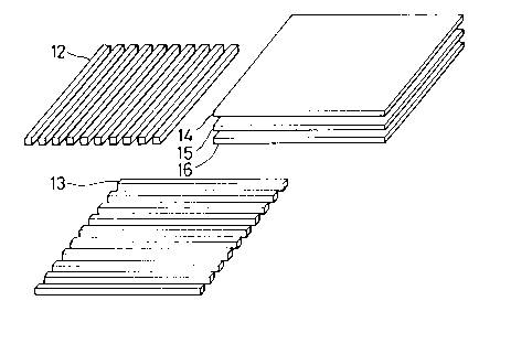
shown in Fig. 3(a), numeral 12 (first dielectric layer) and 13,
a set of 10 pieces were adhered to the first electrode layer 14
and the second electrode layer 15 with an adhesive to form an
upper dielectric layer, and another set of 10 pieces to the
second electrode layer 15 and the third electrode layer 16 with
the adhesive to form a lower dielectric layer, with the strip
pieces of the upper layer crossing the strip pieces of the
lower layer at an angle of 90 degrees. Thus, there were
prepared test samples for Example 4 and Compraative Examples 3
to 5. [Fig. 3(b)] Additionally, as the electrode layers for
the respective samples, aluminum plates of 50 x 50 mm and 1.0
mm in thickness were used and, as the adhesive, an RTV series
adhesive of 30 degrees in hardness was used.
Then, rubber plates 19 and 20 were respectively adhered
to the first electrode layer 14 and the third electrode layer
16 using a pressure sensitive adhesive double coated tape so as
to attain uniform application of pressure and electric
insulation. As the rubber plates 19 and 20, EPT rubber plates
of 50 x 50 mm and 5.0 mm in thickness having a hardness of 60
degrees were used.
Each test sample was connected to the LCR meter in the
same manner as described hereinbefore, and sandwiched between
tensile strength-compression strength measuring members 17 and
2 1 82221
`~ --19--
18 of an all-purpose tensile-compression tester, TCM-1000, made
by Shinko Tsusin Kogyo K.K. Then, measurement was conducted at
a compression-drawing cycle mode of 1 mm per minute up to 240
kg using a load cell of 500 kg in a full scale to obtain graphs
shown in Figs. 15 to 18.
Additionally, Fig. 15 is a graph showing the results of
the measurement of the test sample for Example 4, Fig.16 for
Comparative Example 3, Fig. 17 for Comparative Example 4, and
Fig. 18 for Comparative Example 5.
It has been found from Figs. 15 to 18 that the test
sampie for Example 4 showed the least hysteresis, and the test
sample for Comparative Example 5 showed the largest hysteresis
and that this was in a close relation to the physical
properties of the vulcanized moldings shown in the lower part
of Table 2. This test results reveal that it was only the test
sample of Example 4 that showed a hysteresis of 1 PF.
ZO
2 1 ~222 1
-20-
[Table 2]
Ex.4 Comp. Ex. 3 Comp. Ex. 4 Comp. Ex. 5
Grade #KE9511~ #XE951-U #XE152-U~ #KE650-U~
Catalo- Main Industri- Food pack- Transparent Boots; For
gue- Use al mate- ing; Rubber tubes for sealing use
describ- rial with stopper for beverage; such as 0-
ed high re- medical use; For other rings
Matter sistance Industrial foods
against packing
flexing
fatigue
Hard-50 deg. 50 deg. 50 deg. 50 deg.
ness
*1 4.6 % 10.0 % 18.0 % 36.0 %
Actual Hard-50 deg. 49 deg. 50 deg. 51 deg.
Measure- ness
ments tan ~ 0.016 0.038 0.046 0.065
Impact83 % 68 % 57 % 41 %
resili-
ence
*2 2.5 % 6.2 % 12.3 % 18.7 %
~: manufactured by Shin-etu Kagaku K.K.
*1: compression set mesured at 150 C for 22 hrs.
*2: compression set mesured at 25 C for 22 hrs.
Example 5 and Comparative Examples 6 and 7
Similar tests were conducted using 50-deg. polyurethane
rubbers of caprolactone series described in Table 3. As
polyol, a bifunctional product of a trade name of PCL220N (made
by Daisel Ltd.) having a molecular weight of 2000 and both
terminal hydroxyl groups was used. After dehydrating this
polyol at 120C, it was mixed with an MDI isocyanate product of
a trade name of Milionate MT (made by Nippon Polyurethane K.K.)
2 1 ~22 1
-21-
and a cross-linking agent, TMP, and the resulting mixture was
poured into a mold for producing a pipe-shaped product, then
heated at 100C for 12 hours in an electric furnace to harden.
Thus, there were prepared test materials.
The materials were finish-abraded into a thickness of 1.5
mm using an abrasion machine for rubber, and cut into sheets.
Strip pieces of the same dimensions as in Example 3 were
prepared and disposed at regular intervals to prepare test
samples of Example 5 and Comparative Examples 6 and 7 shown in
Flg. 3(b). These test samples were subjected to the tests in
the same manner as in Example 1 to obtain graphs shown in Fig.
19 to 21.
Additionally, Fig. 19 is a graph showing the results of
Example 5, and Figs. 20 and 21 the results of Comparative
Examples 6 and 7, respectively.
By comparing the results with respect to the physical
properties in Table 3, it was found that the test sample of
Example 5 having good tan ~, impact resilience and compression
set was usable as a pressure sensor. Thus, it was confirmed
that materials having physical properties in accordance with
the present invention were also obtained by using polyurethane
rubber.
Additionally, in each of the above Examples, descriptions
are made by reference to the case where three electrode layers
are provided. It is also possible to provide 5- or more
odd-number electrode layers in parallel to each other, between
each two of which may be provided a dielectric layer, or two
electrode layers may be provided in parallel to each other
between which a dielectric layer is disposed.
21&2221
-22-
[Table 3]
Ex. 5 Comp. Ex. 6 Comp. Ex. 7
Formul- PCL 220N 100.0
ation Milionate MT 21 23 25
TMP 2.6 3.0 3.5
Actual Hardness 60 deg. 59 deg. 60 deg.
Measure- Impact resili- 80 ~ 56 % 42 %
ment ence
tan ~ 0.015 0.039 0.064
Compression
set 2.1 % 8.5% 36.2 %
Another embodiment of the present invention is
specifically described below.
In an embodiment shown in Fig. 22, first dielectric
pieces 9' and second dielectric pieces 10' are provided between
a first electrode layer 53 and a second electrode layer 54.
The first dielectric pieces 9' and the second dielectric pieces
10' are disposed so that their longitudinal direction crosses
at right angles to the paper plane and have a parallelogramic
section taken along the direction crossing at right angles to
the longitudinal direction.
Each of the first dielectric pieces 9' is inclined
rightward at an angle of ~ with respect to the second
electrode layer 54, whereas each of the second dielectric
pieces 10' is inclined leftward at an angle of ~ with respect
to the second electrode layer 54. The first dielectric pieces
9' and the second dielectric pieces 10' are alternately
provided, with the number of the first dielectric pieces 9'
being the same as the number of the second dielectric pieces
10'. Additionally, although the number of the first dielectric
pieces 9' is the same as the number of the second dielectric
pieces in Fig. 22, the numbers may be slightly different from
each other.
When pressure is applied to the first electrode layer 53,
2 1 8222 1
.
-23-
forces to shift the first electrode layer 53 and the second
electrode layer 54 in directions different from the
pressure-applying direction (vertical direction in Fig. 22) are
cancelled out owing to the above-described structure, and the
shearing deformation can effectively be utilized. That is, the
above-described structure serves to prevent the first electrode
layer 53 and the second electrode layer 54 from shifting in a
horizontal direction, thus a pressure sensor showing a wide
region where capacitance changes in a linear manner being
provided.
In addition, a ratio of width (W1) of each of the first
dielectric pieces 9'(or second dielectric pieces 10') in
contact with the first electrode layer 53 (or second electrode
layer 54) to thickness (T1) of the first dielectric layer 9 (or
second dielectric layer 10), i.e., W1/T1, is preferably 2/3.
As to thickness of the first dielectric pieces 9' and the
second dielectric pieces 10' is preferably 0.2 mm to 5 mm,
particularly preferably 1.5 mm, in view of ease of their
production and minimization of scattering in sensitivity of
produced pressure sensors.
Additionally, in practicing this embodiment of the
present invention, as is shown in Fig. 23, N (N = 5 in Fig. 23)
first dielectric pieces 9' inclining at an angle of ~rightward
with respect to the second electrode layer 54 may be provided
on one side, while N (N = 5 in Fig. 23) second dielectric
pieces 10' inclining at an angle of~ leftward with respect to
the second electrode layer 54 may be provided on the o-ther
side.
Further, in order to obtain a practical pressure sensor,
a structure wherein two dielectric layers of dielectric layer
14A and dielectric layer of 14(B) and three electrode layers
15', 16' and 17' sandwiching them are disposed as shown in Fig.
24(A) is preferred since it is scarcely affected by ambient
atmospheric charge upon use, which serves to reduce error of
capacitance upon measurement.
" 2i~2221
_ -24-
Further, in uses where pressure is applied to the
pressure sensor in a non-specific direction, a structure as
shown in Fig. 24(B) wherein the upper dielectric layer 14A and
the lower dielectric layer 14B are so disposed that dielectric
pieces constituting respective dielectric layers cross at right
angles to each other is desirable.
Additionally, in the case of using a rubber elastic body
with a certain formulation where a load to be measured is so
large that the dielectric layer pieces with a parallelogramic
section is deformed out of the region with a good linearity or
where the parallelogramic dielectric layer pieces might
possibly be broken due to too large deformation of the
dielectric layer pieces, it may also be possible to increase
electrode layers 38 and dielectric layers 39 in number to form
a multi-layered structure as shown in Fig. 25(A) to (E) which
serves to reduce the pressure per dielectric layer and prevent
the pressure sensor from being damaged upon a maximum load
being applied thereto. In such case, it suffices to dispose
odd-number electrode layers 38 parallel to each other and each
of the dielectric layers 39 is sandwiched between each two of
them, with odd-number order electrode layers 38 (excluding the
dielectric layers) being connected to each other with a wiring
cord in a parallel connection and connected to one terminal of
an alternating power source, and even-number order electrode
layers 38 (excluding diectric layers) being connected to each
other with a wiring cord in a parallel connection and connected
to the other terminal of the alternating power source.
In order to prevent unnecessary shift at a
pressure-applied area due to searing deformation, the sectional
shape may not be a parallelogram, and dielectric pieces with
various sections 41, 42, 43, 44, 45, and 46 as shown in Fig. 26
(A) to (D) may also be used, with respective dielectric pieces
41 to 46 being used almost in the same number. That is, as is
shown in Fig. 26(A), the sectional shape of the dielectric
pieces may be that wherein ~ = 45 and ~= 90. Thus, the
2 ~ ~222 1
-25-
dielectric pieces may have any sectional shape as long as~ is
in the range of from 30 to 85and ~ is in the range of from 90
to 145 , and those designated by numeral 43 to 46 in Fig.
26(B) and (C) may be employed.
In addition, although, in Fig. 26(A) to (C), the
dielectric pieces of different sections are alternately
provided (i.e., in the order of a dielectric piece 41 and a
dielectric piece 42, or of a dielectric piece 43 and a
dielectric piece 44) in a horizontally simmmetrical manner with
respect to the sectional shape, it is also possible to provide
N (N = 3 in Fig. 26) dielectric pieces 41 directed in the same
direction on one side, and N (N = 3 in Fig. 26) dielectric
pieces 42 on the other side so that the sectional shapes
thereof are symmetrical with each other.
Additionally, in Fig. 26(A) to (D), numeral 50 designates
a first electrode layer, and 40 a second electrode layer.
The manner of disposing the dielectric layers is not
limited to those described above, and those shown in, for
example, Figs. 32 and 33 may also be employed. That is,
dielectric pieces 47 and 48 may be provided at a predetermined
angle of ~ to side 35A of the second electrode layer 35, with
the dielectric pieces 47 and 48 being disposed in a symmetrical
manner with respect to the sectional shape.
Further, as is shown in Figs. 34 and 35, a pair of
dielectric pieces 47 and 48 may be disposed so that the upper
ends of the pieces in Fig. 34 are more spaced than the lower
ends, with this relation being alternately reversed as shown in
Fig. 34.
Still further, as is shown in Figs. 36 to 38, a pair of
dielectric pieces 47 which have a continuously decreasing width
in the downward direction in Fig. 36 (i.e., dimension in the
horizontal direction in Fig. 36) may be provided, with this
relation being alternatelyreversed as shown in Fig. 36.
As to the materials for the dielectric pieces to be used,
it is important for them to have a high impact resilience and a
2 i &222 1
-26-
small compression set, and those with a high impact resilience
and a small compression set such as natural rubber, IR, BR,
polyurethane rubber, silicone rubber, etc. may be employed.
A lower rubber hardness provides a higher spring
constant, whereas a higher rubber hardness provides a higher
spring constant. Thus, for example, dielectric pieces for
manufacturing various general-purpose pressure sensors whose
maximum measurable loads are from about 10 kg to 1000 kg may
use rubbers with a rubber hardness of 20 degrees to 80 degrees
in terms of scale A described in JIS-K-6301 taking the spring
constant, shape, area, and other factors into consideration.
Assuming the case of manufacturing a pressure sensor
whose maximum measurable load is about 100 kg and which is
designed for measuring pressure force of rubber rolls in a
printng press, a rubber with a rubber hardness of 30 degrees to
40 degrees in terms of scale A described in JIS-K-6301 is
preferably used for the dielectric pieces and, as a material
for the dielectric layer, a silicone rubber is one of the
optimal materials due to its good rubber elasticity, less
change in spring constant with time, and less change in spring
constant upon temperature being changed.
Examples 6 and 7, and Comparative Examples 8 to 10
In order to confirm the relation between shape and
output, the following tests were conducted using the same
rubber material, the same rubber hardness, and the same area to
which pressure was applied.
As a rubber for the dielectric layer, polybutadiene
rubber having the formulation shown in Fig. 4 was used. This
was subjected to electrical heat press molding under the
conditions of 165~ x 15 minutes and 200 kg/cm2 to prepare a
vulcanized rubber sheet of 1.5 mm in thickness, 150 mm in
width, and 200 mm in length. This sheet had a rubber hardness
of 40 degrees in terms of scale A described in JIS-K-6301.
Then, this rubber sheet was cut into 5 kinds of strip
~182221
-27-
pieces (dielectric pieces) respectively having sectional shapes
shown in Table 5, No. A to No. E (shapes taken along the plane
crossing at right angles to the longitudinal direction) without
changing thickness and length. The strip pieces No.A to No.E
were respectively adhered to the first electrode layer 15',
second electrode layer 17', and third electrode layer 17' shown
in Fig. 24(C) parallel to each other. Additionally, each
electrode was made of an aluminum plate of 200 mm in width, 250
mm in length, and 5 mm in thickness. This adhesion was
conducted as shown in Fig. 24(A) so that an area to which
pressure is to be applied of the dielectric layers 14A and 14B
[sum of the contact areas between one side of the dielectric
piece constituting the dielectric pieces 14A (or 14B) and the
electrode layer] was equally 60 cmZ with No.A through No.E (see
Table 6) using the aforesaid strip pieces (dielectric pieces)
in the number described in Table 6 and an urethane series
two-part adhesive.
Thus, there were prepared 5-layered test samples having
two dielectric layers and three electrode layers as shown in
Fig. 27(A) to (E), i.e., test sample No. T-1 (Comparative
Example 8), No. T-2 (Comparative Example 9), No. T-3
(Comparative Example 10), No. T-4 (Example 6), and No. T-5
(Example 7).
Additionally, numerals 27' and 29' in Fig. 27 (A) to (E)
represent a first dielectric layer and a second dielectric
layer, respectively. Signs 27A and 27B in Fig. 27(D) represent
a first dielectric piece and a second dielectric piece in the
first dielectric layer 27', respectively, and signs 29A and 29B
represent a first dielectric piece and a second dielectric
piece in the first dielectric layer 29', respectively. Signs
27C and 27D in Fig. 27(E) represent a first dielectric piece
and a second dielectric piece in the first dielectric layer
27', respectively, and signs 29C and 29D epresent a first
dielectric piece and a second dielectric piece in the first
dielectric layer 27', respectively. Additionally, Fig. 24(A)
21 & L 221
--28--
shows an example prepared by using the strip pieces 14A (14B)
shown in Fig. 24(D) (No. T-3).
Then, each of the test samples No. T-1 to T-5 was
connected to a precision LCR meter, HP4284, made by Huret
Paccard Co. in such manner that , as is shown in Fig. 28, the
first electrode layer 15' and the third electrode layer 17'
were connected to one output terminal 22' of the precision LCR
meter via a connecting portion 20' using wire cords 18' and
19', respectively, and the remaining second electrode layer 16'
was connected to the other output terminal 23' of the LCR meter
through a wire cord 21'. An alternating current voltage of 1
MHz 6 V was applied thereacross, and a 20-kg weight or weights
25' were placed in piles on each of the samples (first
electrode layer 15') (see Fig. 28) to apply loads of 0 kg, 20
kg, 40 kg, 60 kg, 80 kg, and 100 kg. Capacitance of each test
sample under each load was measured. The results thus obtained
are shown in Table 7 and Fig. 29.
As is apparent from Table 7 and Fig. 29, changing amounts
of capacitance with the test sample of Example 6 (sectional
shape: diamond shape) and the test sample of Example 7
(sectional shape: parallelogram) are clearly different from
those with the test samples of Comparative Examples 8 to 10
having the same contact area with the electrode layer and
undergoing simple compression, thus the test samples of
Examples 6 and 7 being proved to have a sensitivity several
times as much as the test samples of Comparative Examples 8 to
10. In the case of simple compression, the test sample of
Comparative Example 9 (W/T = 2.0) is said to be a limit of not
suffering abnormal deformaton or falling down upon being
pressed, thus the test sample of Comparative Example 10 is not
used in simple compression. To compare to the test sample of
Comparative Example 9 which is most popular for simple
compression, the test sample of Example 8 (W/T = 1) was found
to show a 4-fold changing amount, and the test sample of
Example 7 (W/T = 2/3) a more than 5-fold changing amount.
2 1 ~222 1
-29-
[Table 4]
Compounded Chemicals Parts by Weight
JSR-BR-01 100.0
Active zinc flower 5.0
Stearic acid 0.5
Aging inhibitor 3C 0.5
Percumyl D-40 6.0
Diana PX-50 8.0
Nipsil VN3 2
Precipitated sulfur 1.0
[Table 5]
No. Sectional Shape of Dielectric Pieces
A Rectangle;
1.5 mm thick; 1*~3~
6 mm wide
B Rectangle;
1.5 mm thick; ~k~
3 mm wide
C Rectangle;
1.$ mm thick;
1.5 mm wide
D 45 deg. Diamond;
1.5 mm thick;
1.5 mm wide
E 45 deg. Parallelogram;
1.5 mm thick;
1.0 mm wide
2i8~221
- -30-
[Table 6~
Shape of Rubber Number Pressure-
used in Each Test of Ru- applied
Sample (Dielectric bber per Area
Layer described in Layer of
Table 5) Sample
Comp. Ex. 8 No.A (rectangle) 5 60 cmZ
(No.T-1)
Comp. Ex. 9 No.B (rectangle) 10 60 cm2
(No.T-2)
Comp. Ex. 10 No.C (square) 20 60 cm2
(No.T-3)
Example 6 No.D (diamond) 30 60 cm2
(No.T-4)
Example 7 No.E (parallelo- 30 60 cmZ
(No.T-4) gram)
[Table 7]
Test Results for Examples 6 and 7, and Compara-
tive Examples 8 to 10 (Change in capacitance (Cp)
for respective loads; and rate of change taking
change in Comparative Ex. 8 as 1; provided that
numerals are presented in terms of pico-farad
(Cp) )
Load Okg 20 kg 40 kg 60 kg 80 kg 100 kg
~Cp ACp * dCp * ~Cp * ~Cp * ~ Cp *
Comp. Ex. 8 0.0 4.8 1.0 9.2 1.0 13.3 1.0 16.8 1.0 18.5 1.0
(No.T-1)
Comp. Ex. 9 0.0 12.0 2.5 22.4 2.4 31.6 2.4 39.0 2.3 43.6 2.4
(No.T-2)
Comp. Ex. 10 0.0 15.8 3.3 30.1 3.3 43.2 3.2 54.1 3.2 61.4 3.3
(No.T-3)
Example 6 0.0 32.0 6.7 63.1 6.9 95.6 7.2129.6 7.7159.6 8.6
(No.T-4)
Example 7 0.0 38.3 8.0 75.7 8.2114.7 8.6154.5 9.2191.0 10.3
(No.T-5)
2 1 ~222 1
,
-31-
*: rate of change
Examples 8 to 10, and Comparative Examples 11 and 12
As a test for making practicable by more increasing the
rate of change in capacitance, tests were conducted using
silicone rubbers having a good heat resistance and a good cold
resistance and a less temperature dependence to examine how
rubber hardness, pressure-applying area, and shape exert
influences on capacitance in comparison with standard simple
compression shape. Table 8 describes sectional shape of
dielectric pieces constituting the dielectric layers of
respective Examples and Comparative Examples, sectional shapes
of tested samples, and contact areas between the dielectric
pieces and the electrode layer.
The used silicone rubber is a dimethylsilicone rubber of
existing grade. That is, #KE941U (40 deg.) and #KE931U (30
deg.) made by Shin-etu Kagaku K.K. were compounded in a manner
specified by the manufacturer, and kneaded in an oven roll to
prepare a raw rubber. Three test samples for No. T-8 (Example
8), No. T-9 (Example 9), and No. T-10 (Example 10) which were
expected to show large change in capacitance from the results
shown in Table 8 were prepared as follows.
That is, as is shown in Figs. 30(A) and (B), dielectric
pieces 31 and 34 of Examples 8 to 10 were disposed on and
beneath a second electrode layer (35) composed of a 0.2-mm
thick stainless steel sheet, SUS#301, in a symmetrical manner
with respect to sectional shape, and adhered via an adhesive
using a newly made special press molding under the molding
conditions of 170C, 10 minutes, and 200 kg/cm2 to prepare
intermediate products. Fig. 30(A) is a plan view from above of
the intermediate products, and Fig. 30(B) a side view thereo~.
Each of the intermediate products was adhesively
sandwiched so that a 1-mm thick, aluminum-made first electrode
layer 36 was on the upper side, and a 1-mm thick, aluminum-made
second electrode layer 37 on the lower side through an RTV
2i8~221
-32--
silicone rubber of 30 deg. in rubber hardness to prepare test
samples shown in Fig. 30(C). Fig. C is a sectional view of the
test sample.
Two test samples of Comparative examples 11 and 12 for
comparison having a simple compression shape were prepared as
follows. A 1.5-mm thick press-molded sheet composed of
silicone rubber was prepared in the same manner as in Example
6, and cut into strip pieces having a rectangular section as
with test sample Nos. T-6 and No. T-7 in Table 8.
Then, the strip pieces were adhered in the same manner as
in Example 6 to prepare test samples. Additionally, as an
adhesive, the same RTV silicone rubber of 30 deg. in rubber
hardness as used for Nos. T-8 to T-10 was used. Five kinds of
the test samples for Nos. T-6 to T-10 were additionally heated
in an electric furnace at 200C for 4 hours to stabilize their
physical properties.
Each of the above-described test samples was tested in
the same manner as in Example 1. Results thus obtained are
shown in Table 9 and Fig. 31.
It is seen from the results, that the test sample of
Example 10 having a pressure-applied area of 40 cm2 which is
smaller than 60 cmZ in Example 6, etc. and having a rubber
hardness of 30 degrees shows change in capacitance of about 5
times as much as that of the test sample of average smple
compression and of 40 degrees in ruber hardness (test sample of
Comparative Example 11), thus much greater change in
capacitance being confirmed in comparison with the conventional
one.
Additionally, when a pressure sensor for measuring
pressure of pressure rolls in a printing press was made using
the test sample of Example 10, it showed a change of 245 PF
under a load of 100 kg with an enough linearity. Thus, it
becomes possible to make a pressure sensor capable of measuring
up to 100 kg which is composed of a dielectric layer (made of
rubber) of at least 1 PF = 0.5 kg and electrode plates and
2 ~ &222 1
_ -33-
which is difficult to break and can be made inexpensively.
[Table 8]
Dielectric Piece Sectional Shape of Test Pressure-
Sample applying
Rubber Dimension Odd-number Order...Electrode Area
Hard- and Shape Layer
ness of Sec- Even-number OrderDielectric
tion Layer
Comp.
Ex.11 40 Rectangle If ~f,~f~',y,.~ "';'~/;f~
(No. deg. ;1.5 mm ~ sr~ ) 60 cm2
T-6) thick 3 0
mm wide
Comp.
Ex.12 30 Rectangle l/f~ x/-f~f~
(No. deg. jl.5 mm ~ 60 cmZ
~ 5~ J~
T-7) thick; 3.0 ti'~'~ ,f "~
mm wide
Ex. 8 30 Parallelo-
(No. deg. gram; 1.5 60 cm2
T-8) mm thick; I~ /"/,//i
1 0 mm wid~ ~ -
(angle ofl~ /,',ff,~ ff/~
- inclination
~ = 45 )
Ex. 9 30 Parallelo-
(No deg gram; 1 5 50 cm2
T-9) mm thick; If~ -''.;',fi~f~ff,f".,~f~f/',':' ~ t
1.0 mm wid~
(angle of l';.'~ , f; ' ',~ f ',f'~
inclination
~ = 45 )
2 1 &222 1
_ -34-
(contd.)
Ex.10 30 Parallelo-
(No. deg. gram; l.S 40 cmZ
I"~"~J~'"~"~ "f~
T-10) mm thick; ~a
1.0 mm wide
(angle of -
inclination
~ = 45 )
10 [Table 9]
Test Results for Examples 8 and 9, and Compara-
tive Examples 11 and 12 (Change in capacitance
(Cp) for respective loads; and rate of change
taking change in Comparative Ex 8 as 1;
provided that numerals are presented in terms of
pico-farad (Cp))
Load 0 kg¦ 20 k~J 40 k~J 60 kg 80 kg 100 kg
~ Cp f~ Cp * f1Cp * ~Cp * f~Cp * ~ Cp *
Comp. Ex.11 0.0 12 8 1 0 24.1 1.0 33.8 1.0 40.9 1.0 46.1 1.0
(No.T-6)
Comp. Ex.12 0.0 15.1 1.2 28.4 1.2 39.9 1.2 49.2 1.2 56.4 1.2
(No.T-7)
Example 8 0.0 39.2 3.1 75.8 3.1117.4 3.5152.8 3.7187.0 4.1
(No . T-8 )
Example 9 0 0 45 6 3 6 91.2 3 8132. 8 3.9174.6 4.3217.6 4.7
(No.T-9)
Example 10 0.0 55 2 4.3103.6 4.3152.8 4.5202.3 4.9245.0 5.3
(No.T-10)
*: rate of change
[Advantages of the Invention]
According to the present invention, there is provided a
pressure sensor capable of measuring weight or pressure with
high accuracy without any complicated structure.
21 ~221
_ -35-
[Brief Description of the Drawings]
Fig. l(a) is a perspective view of a dielectric layer.
Fig. l(b) is a sectional view of a pressure sensor
wherein dielectric layer pieces disposed as an upper layer and
a lower layer are parallel to each other.
Fig. l(c) is a perspective view of electrode layers.
Fig. 2 is a perspective view showing the state of
measuring capacitance of a pressure sensor.
Fig. 3(a) is an analyzed perspective view of a pressure
sensor.
Fig. 3(b) is a perspective view of a pressure sensor.
Fig. 4 is a perspective view showing the state of
measuring capacitance of a pressure sensor.
Fig. 5 is a graph showing the relation between load
applied to the pressure sensor of Example 1 and change in
capacitance.
Fig. 6 is a graph showing the relation between load
applied to the pressure sensor of Example 2 and change in
capacitance.
Fig. 7 is a graph showing the relation between load
applied to the pressure sensor of Example 3 and change in
capacitance.
Fig. 8 is a graph showing the relation between load
applied to the pressure sensor of Comparative Example 1 and
change in capacitance.
Fig. 9 is a graph showing the relation between load
applied to the pressure sensor of Comparative Example 2 and
change in capacitance.
Fig. 10 is a graph showing the relation between load
applied to the pressure sensor of Example 1 and change in
capacitance.
Fig. 11 is a graph showing the relation between load
applied to the pressure sensor of Example 2 and change in
capacitance.
Fig. 12 is a graph showing the relation between load
2 i &~22 1
-36-
applied to the pressure sensor of Example 3 and change in
capacitance.
Fig. 13 is a graph showing the relation between load
applied to the pressure sensor of Comparative Example 1 and
change in capacitance.
Fig. 14 is a graph showing the relation between load
applied to the pressure sensor of Comparative Example 2 and
change in capacitance.
Fig. 15 is a graph showing the relation between load
applied to the pressure sensor of Example 4 and change in
capacitance.
Fig. 16 is a graph showing the relation between load
applied to the pressure sensor of Comparative Example 3 and
change in capacitance.
Fig. 17 is a graph showing the relation between load
applied to the pressure sensor of Comparative Example 4 and
change in capacitance.
Fig. 18 is a graph showing the relation between load
applied to the pressure sensor of Comparative Example 5 and
ZO
change in capacitance.
Fig. 19 is a graph showing the relation between load
applied to the pressure sensor of Example 5 and change in
capacitance.
Fig. 20 is a graph showing the relation between load
applied to the pressure sensor of Comparative Example 6 and
change in capacitance.
Fig. 21 is a graph showing the relation between load
applied to the pressure sensor of Comparative ~xample 7 and
change in capacitance.
Fig. 22 is a sectional view showing one speci~ic example
of a second embodiment of the present invention.
Fig. 23 is a sectional view showing another specific
example of the second embodiment of the present invention.
Fig. 24(A) is a side view of a pressure sensor.
Fig. 24(B) is a perspective view of a pressure sensor
21 ~222 1
_ -37-
wherein the upper dielectric pieces are disposed at right
angles to the lower dielectric pieces.
Fig. 24(C) is a perspective view of electrode layers.
Fig. 24(D) isa perspective view of dielectric pieces.
Fig. 25(A) to (E) are sectional views of pressure sensors.
Fig. 26(A) to (D) are sectional views of pressure sensors.
Fig. 27(A) to (E) are sectional views of pressure sensors.
Fig. 28 is a perspective view showing the state of
measuring capacitance of a pressure sensor.
Fig. 29 is a graph showing the relation between load and
capacitance.
Fig. 30(A) is a plan view of a pressure sensor before a
first electrode is applied thereto.
Fig. 30(B) is a side view of (A).
Fig. 30(C) is a sectional view of a pressure sensor after
the first electrode layer is applied thereto.
Fig. 31 is a graph showing the relation between load and
capacitance.
Fig. 32 is a plan view of a pressure sensor before a
first electrode is applied thereto.
Fig. 33 is a side view of Fig. 32.
Fig. 34 is a plan view of a pressure sensor before a
first electrode is applied thereto.
Fig. 35 is a side view of Fig. 34.
Fig. 36 is a plan view of a pressure sensor before a
first electrode is applied thereto.
Fig. 37 is a view of the pressure sensor of Fig. 36
viewed from one longitudinal direction of the dielectric layer.
Fig. 38 is a view of the pressure sensor of Fig. 36
viewed from the other longitudinal direction of the dielectric
layer.
Fig. 39 is a sectional view of a conventional pressure
sensor.
Fig. 40 is a graph showingthe relation between load and
change in capacitance with respect to a conventional pr-essure
`~ 21&2221
----3 8
sensor .