Note: Descriptions are shown in the official language in which they were submitted.
- 2 1 82852
SHIELD ASSEMBLY AND METHOD OF SHTPT nING SUITABLE FOR
USE IN A COMMUNICATION DEVICE
Background of the Invention
1. Field of the Invention
The present invention relates generally to an electrical assembly
and more particularly to an assembly for shielding an electronic circuit
disposed on a substrate from inle~ference.
20 2. Description of the Related Art
Modern electronic equipment includes electrical circuits
mounted on a substrate that are sensitive to electromagnetic
intelrelellce (EMI) and radio frequency inleLfelellce(RFI) (collectively,
25 inLelrer~llce). InLelference may originate from internal sources within
the electronic equipment or from external intelfeL~nce sources.
InLe~rence can cause degradation or complete loss of important
signals, rendering the electronic equipment inefficient or inoperable.
To minimize il~Lelfer~l~ce, electrically conducting material is
30 interposed between portions of the electrical circuit. For
manufacturability purposes, this material is tooled into multiple
enclosures or shields that conform to the electrical circuits. These
shields are attached, typically via soldering, to grounded traces
positioned both on the substrate and around the electrical circuits
- - 2 1 82852
--2-
generating the inlelfel~nce as well as around the electrical circuits that
are susceptible to inLelfeLellce. Oflenl,mes~ the shields are attached in
adjacency.
Techniques for adjacently attaching such shields include
providing dual traces (a separate trace for each shield) and providing a
single trace that is shared by both shields. However, dual traces
consume an unacceptable amount of physical space. For example,
assuming that each trace is 1.00 mm wide and each trace is separated by
a 0.26 mm gap to ensure reliable attachment, dual traces-require at least
2.26 mm of substrate area. Unfortunately, a single, shared trace has
been found to be too unreliable. During attachment of the shields to a
shared trace, such as the aforementioned 1.00 mm trace, the solder
exhibits capillary attraction and migrates from the trace onto one or
both shields. This leaves an insufficient amount of solder at the trace-
shield interconnection thereby preventing reliable attachment. When
sharing a trace as such the shields also tend to skew and even walk off
the trace during attachment.
As portable electronic equipment becomes increasingly
miniaturized and components of electrical circuits are placed closer
together, the physical room available for shielding is greatly reduced.
Therefore, what is needed is a shield assembly and a method of
shielding that consumes as little space as possible and provides secure,
reliable, and easily manufacturable interconnections.
Brief Description of the Drawings
FIG. 1 illustrates a radio communication system including a
portable electronic device employing a shielding assembly;
FIG. 2 illustrates an exploded perspective view of the shielding
assembly of FIG. 1;
FIG. 3 illustrates a consolidated perspective view of the shielding
assembly of FIG. 1; and
2 1 82~52
FIG. 4 illustrates an enlarged fragmentary plan view of the
shielding assembly of FIG. 3.
Detailed Description of the Plere~led Embodiments
A shielding assembly for shielding an electronic circuit disposed
on a substrate includes traces and a shield. The traces are disposed on
the substrate about the electronic circuit. The shield includes leads for
attachment to the traces. The shield is attached to the traces such that
some of the leads, which are staggered, attach to the traces in a
nonconsecutive manner. An additional shield including alternately
staggered leads can be adjacently attached to the previously attached
shield. This is accomplished by attaching the alternately staggered leads
of the additional shield to those traces that are between the traces
attached to the previously attached shield.
FIG. 1 illustrates a radio communication system including a
portable electronic device, specifically a portable radiotelephone 100,
employing a shielding assembly 102. The portable radiotelephone 100
includes a housing 104, an antenna 106 carried on the housing 104, a
substrate 107 disposed within the housing 104, and a transceiver circuit
108 disposed on the substrate 107 beneath the shield assembly 102. A
speaker (not shown), a microphone (not shown), a keypad (not shown),
and a display (not shown) are disposed on a front side of the housing
104 that is hidden from view in FIG. 1. The portable radiotelephone
100 is powered by a detachable battery 110 attached to the housing 104.
The portable radiotelephone 100 operates in a radiotelephone
communication system by communicating with a fixed site transceiver
112 via radio frequency (RF) signals 114. The fixed site transceiver 112
transmits the RF signals 114 into a radio coverage area populated by the
portable radiotelephone 100. The antenna 106 transduces the RF
signals 114 into electrical RF receive signals and couples the electrical
RF receive signals to the transceiver circuit 108. The transceiver circuit
108 transforms the electrical RF receive signals into data receive signals
2 1 ~32852
-4-
which are then output to the user as audible speech via the speaker and
as operational information via the display. Speech and data input by
the user via the keypad and the microphone, respectively, is coupled to
the transceiver circuit 108 as data transmit signals. The transceiver
5 circuit 108 converts the data transmit signals into electrical RF transmit
signals which are transduced by the antenna 106 and transmitted to the
fixed site transceiver 112 as the RF signals 114.
The shielding assembly 102, which is only partially shown in
FIG. 1, includes a plurality of shields 116 and a plurality of traces 118
10 disposed on the substrate 107. The plurality of shields 116 are
electrically connected to the plurality of traces 118 to substantially
enclose the transceiver circuit 108. The shielding assembly 102
prevents inLeLrerence, such as electromagnetic inlelferellce (EMI) and
radio frequency intelfer~nce (RFI), from radiating beyond or
15 penetrating through the plurality of shields 116 and inLerr~lillg with
the operation of the transceiver circuit 108 by, for example, degrading
the aforementioned electrical RF receive and transmit signals as well as
the data receive and transmit signals.
Although illustrated in a portable radiotelephone, the shielding
20 assembly 102 will also find application in virtually any electronic
apparatus, including computers, cordless telephones, two-way radios,
pagers, personal digital assistants, and the like.
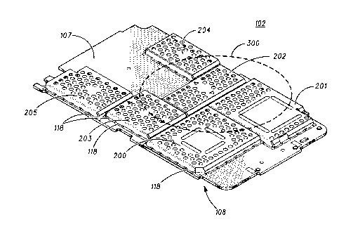
FIG. 2 illustrates an exploded perspective view of the shielding
assembly 102 wherein the plurality of shields 116 are shown detached
25 from, and projected above, the plurality of traces 118. In a ~rerelled
embodiment, the shield assembly 102 includes shields 200-205. Each
one of shields 200-205 includes a planar top surface and substantially
orthogonal side portions that extend downwardly therefi;)lll and
terminate in a bottom edge periphery. A plurality of leads extend
30 downwardly from the bottom edge periphery in planarity with the side
portions. The plurality of leads are located at predetermined locations
about the bottom edge periphery beneath the side portions.
Shields 200-205 are prereLably fabricated, using a known
progressive stamping technique or a known slide tool technique, from
-- - 2 1 ~2852
-5
a 0.05 mm to a 0.30 mm thick sheet of a nickel-silver alloy, a tin-plated
steel, or other suitable material. The side portions are then folded into
position based on the maximum height of the portion of the
transceiver circuit 108 that is to be shielded. Depending on the type of
components comprising this portion of the transceiver circuit 108, the
height of the side portioris might be less than 3.0 mm.
The plurality of traces 118 are arranged around the transceiver
circuit 108 in rows. The length of the rows correspond to the
dimensions of shields 200-205 and, specifically, to the lengths of their
10 side portions. The plurality of rows extend both transversely and
longitudinally on the substrate 107 and, in a prefe~led embodiment,
partition the transceiver circuit 108 into circuit partitions 206-211. The
circuit partitions 20~211 include a portion of the transceiver circuit 108,
which might be, for example, an oscillator circuit, a microstrip
transmission line, or a power amplifier circuit. Such partitioning
increases manufacturability, eases repairability, and separates
inlerfele~ce producing circuitry from sensitive circuitry.
The plurality of traces 118, which are preferably comprised of
copper trace, are fabricated using known bonding and plating
20 techniques during construction of the substrate 107, which preferably
comprises printed circuit board material, such as polyimide or epoxy-
based flame retardant industrial fiberglass (G10-FR4) The plurality of
traces 118 are electrically coupled to a ground plane (not shown). In the
preferred embodiment, the plurality of traces 118 are 1.00 mm wide so
25 as to ensure an effective metallurgical connection between the plurality
of leads of shields 200-205 and the plurality of traces 118. It will be
recognized, however, that this 1.00 mm width could be varied in
accordance with, for example, variations in the thickness of the
plurality of leads. Each of the plurality of traces 118 are preferably
30 separated from one another by at least 0.26 mm of solder mask barrier
or bare substrate material. The length of each one of the plurality of
traces 118 is slightly larger then the length of the corresponding
plurality of leads of shields 200-205.
- - 2 1 82852
-
--6
The shield assembly 102 is preferably assembled via an
automated assembly process. Initially,-the substrate 107 is subjected to a
screening process that deposits a predetermined amount of solder paste
on the plurality of traces 118. To ensure secure attachment, the
amount of solder (and the size of the plurality of traces 118) should be
sufficient to allow solder to "wick" or adhere on both sides of each of
the plurality of leads of shields 200-205 during reflow. In the preferred
embodiment, the solder paste is a tin-lead-silver alloy.
Next, shields 200-205 are then lowered to enclose circuit
partitions 206-211, respectively, as telegraphed by lines 212. The
plurality of leads of shields 200-205 are positioned into engagement
with the plurality of traces 118, ~refelably by an automated part
placement machine. Unlike large one-piece shields that cover an
entire substrate, shields 200-205 are manageably sized to allow
automated placement by the same large part placement machine that
might, for example, auto place a power amplifier or microprocessor.
Upon positioning shield 200 to enclose circuit partition 206, a complete
set of leads 214 of shield 200 engages all of corresponding ones of the
plurality of traces 118 of row 216. Shield 200 also includes a first set of
staggered leads 218 that are visible through a cut-away portion of the
top surface of shield 200. The first set of staggered leads 218 are spaced
apart and engage only approximately every other one, or
nonconsecutive ones, of corresponding ones of the plurality of traces
118 of row 220.
Such nonconsecutive engagement permits shields 200-205 to
share a common row when adjacently positioned. For example, upon
positioning shield 201 to enclose circuit partition 207, shield 201 is
adjacently positioned to shield 200 and includes a second set of
staggered leads 222 that are spaced apart to engage the remaining
unengaged ones of the plurality of traces 118 of row 220. Shield 201
includes a third set of staggered leads 224 that are visible through a cut-
away portion of the top surface of shield 201. The third set of staggered
leads 224 are spaced apart to engage only approximately every other one
of corresponding ones of the plurality of traces 118 of row 226. Upon
- 2 1 82852
positioning shield 202 to enclose circuit partition 208, shield 202 is
adjacently positioned to shield 201 and~includes a fourth set of
staggered leads 228 that are spaced apart to engage the remaining
unengaged ones of the plurality of traces 118 of row 226. Similarly,
shields 200 and 203 share row 230, shields 202 and 203 share row 232,
shields 202 and 204 share row 234, and shields 203 and 205 share row
236.
After such engagement, the shield assembly 102 is reflow heated
up to a temperature that is sufficient to melt the solder paste to a
liquidus state. The liquidus solder wicks up on both sides of the single
lead that occupies each one of the plurality of traces 118 and forrns an
effective metallurgical interconnection therebetween. In the preferred
embodiment, the shield assembly 102 is reflow heated for
approximately 660 s. During this time period, the temperature of the
shield assembly 102 is increased to approximately 218 ~C.
The shielding assembly 102 is shown fully assembled in FIG. 3.
Shields 200-205, which enclose circuit partitions 206-211, are grounded
and conductive thereby preventing EMI and RFI from radiating
therebeyond or from penetrating therethrough to interfere with the
portions of the transceiver circuit 108 therebeneath. The plurality of
leads of shields 200-205 and the plurality of traces are attached in one-
to-one correspondence. Each one of the plurality of leads is isolated on
its own trace. Shields 200-205 include a plurality of holes to permit
visual inspection of the portions of the transceiver circuit 108
therebeneath. Such holes are sufficiently small enough (one-eighth
wavelength or less at the highest frequency for which shielding is
necessary) to prevent passage of inle~ing EFI or RFI. The size of the
holes of shields 200-205 can be varied based on the sensitivity of the
portion of the transceiver circuit 108 therebeneath. For more sensitive
circuitry, the diameter of the holes are made smaller. Distal
separations between the plurality of leads and openings between the
bottom edge periphery of shields 200-205 and the skipped ones of the
plurality of traces 118 are similarly constrained.
- 2 1 82852
-8-
The nonconsecutive engagement of a shared row of traces by the
plurality of leads of two or more adjacent shields is clearly shown in
FIG. 4, which shows an enlarged illustration of fragment 300 of the
shielding assembly 102 of FIG. 3. For clarity, shields 200-204 are
pictured in dotted line and the land pattern created by the plurality of
leads are pictured in heavy line. Shields are positioned so that their
adjacent side portions are offset from a center or a midline of the
shared row. For example, shield 200 is positioned just to the left of the
midline of row 220 and shield 201, which is adjacent thereto, is
positioned just right of the midline of row 220. The plurality of
staggered leads from each of the shields alternately engage the traces of
the shared row in a staggered land pattern. For example, first and
second leads 401, 402 of the first set of staggered leads 218 of shield 200
engage second and fourth traces 421, 423 of row 220 just to the left of
midline thereof. First, second, and third leads 410, 411, 412 of the
second set of staggered leads 222 of shield 201 engage first, third, and
fifth traces 420, 422, and 424 of row 220 just to the right of midline
thereof.
Although illustrated as substantially rectangular with linear side
portions, it will be recognized that shields 200-205 could be formed into
other geometric shapes, such as circular or semi-circular shapes that
include curvilinear side portions. Although the rows of the plurality
of traces 118 are illustrated as straight lines, it will be recognized that
the term "row" as used herein refers to "a single trace or multiple
traces placed next to each other" and, thus, would include traces that
are offset about a straight line and traces arranged in curvilinear
patterns.
The shield assembly and method of shielding disclosed herein
require only a single row of traces to effectuate attachment of adjacent
shields. The adjacent shields are offset from the midline of the single
row and include staggered leads that alternate attachment to the traces
of the single row. The present shield assembly realizes more than a
50% reduction in the amount of substrate space that was previously
required for shielding assemblies that required dual rows of traces to
- 2 1 82852
g
adjacently attach shields. The one-to-one correspondence between
shield leads and traces of the present shield assembly, avoids field
reliability and skewing problems prevalent in prior assemblies that
attached adjacent shields to the same trace.
What is claimed is