Note: Descriptions are shown in the official language in which they were submitted.
Y
1
GOMPAGm ANTS FABRrCAmrOhT mOr Ff AN~'
T;rGH ~PRED Drl=rm~r. OpmrrnL v_ emrmrsma
BACICGROLTr?D OF THE rNVEN~rrnN
1. Rield of the invention
This invention relates to optical switches, and in
particular to Y-branch digital optical switches.
2. Description of the l2eiaGed Air
Digital Optical Switches (DOS) are increasingly
replacing other types of optical switches in a wide
variety of applications, including communications
systems. One of the most popular digital optical
switches is the Y-branch DOS that has received wide
commercial acceptance primarily because of its robustness
to variations in critical parameters, such as
polarization, wavelength, temperature, and to a large
extent, even the_device geometrical variations.
Typically, a Y-branch DOS is designed such that two
waveguide branches intersect to define a Y-shape
structure with a very small angle at the intersection of
the branches. The composition of the waveguide structure
may include a wide variety of materials, such as lithium
niobate, and semiconductors, to name a few. A Y-branch
DOS performs its switching function by adiabatically
changing (i.e. slowly varying, as opposed to abruptly
altering) the light propagation direction in one of the
waveguidea. Specifically, switching in a Y-branch DOS
is achieved by forcing a refractive-index change in one
waveguide branch with respect to the other. The change
~ 2~8318~
Z
in refractive index may be induced by applying, for
example, voltage and/or -current to selected sections of
the structure. Of particular significance among the
characteristics of a Y-branch DOS is its step-like
responses to applied voltage or current which allow the
light to remain in a higher index branch, notwithstanding
increases in the applied voltage or current beyond a
given threshold. -Hence, by operating the Y-branch DOS
beyond some threshold value for applied voltage/current,
the variations in polarization, wavelength, etc.
mentioned above do not impact the switching capacity of
the Y-branch DOS.
In spite of all the advantages offered by Y-branch
DOS, certain shortcomings of those devices may prevent
their-use in certain applications. For example, the
relatively high voltage drive needed to power lithium
niobate-based Y-branch DOS limits their operative
bandwidth since microwave power increases with applied
voltage. Equally bothersome is the relative oversized
length of the prior-art Y-branch DOS, which increases
overall optical loss for these devices, and hampers their
integration with other devices because of their longer
"footprints". As mentioned above, the gradual and small
changes in the light propagation-direction to achieve the
switching function iri a Y-branch DOS dictate the small
angle and long footprint structure (to avoid crosstalk)
of the prior azt_-Y-branch.DOS. Prominent among the
limitations of the small angle, long-footprint design of
Y-branch DOS is the difficulty in the fabrication of
~ ~:183I86
3
these devices to use conventional photolithographic
techniques to define the small (for example, leas than
.25 micron) separation at the vertex of the two
waveguiding branches of the.Y-branch DOS.
In an attempt to .overcome the limitations of Y-
branch DOS devices, Okayama et al., in an article
entitled "Reduction of Voltage-Length Product for Y-
Branch Digital Optical Switch", published in JOURNAL OF
LIGHTWAVE TECHNOLOGY, VOL. 11, NO. 2, 1983, pp. 379-387,
proposed a two-angle shaped Y-branch DOS that provided
enhanced crosstalk performance, reduced length and lower
voltage drive for a Y-branch DOS. An example of the
Okayama two-angle shaped Y-branch DOS is shown in FIG. l,
wherethe Y-branch DOS 10 has a first waveguide portion
12 connected to intermediate waveguide portions 14, 16 at
a vertex 18, with each of intermediate waveguide portions
14, 16 associated with a first taper angle 81 and
symmetrical about a longitudinal axis 20 of the first
waveguide portion 12.
Each of second waveguide portions 22, 24 is
respectively connected to the first waveguide portions
14, 16 and associated with a second taper angle A,. In
this DOS 10, 6z < 61 to form the tapered Y-branch
configuration. Each of waveguide portions 12-16 and 22-
24 may have identical_widths w, and the configuration 10
may be symmetrical about the longitudinal axis 20.
Other prior-art techniques modified the Okayama
two-angle design to further reduce the length, the
voltage/current drive and cross-talk degradation of a Y-
~~18~1~~
4
branch DOS. Unfortunately, all the prior-art techniques
do not change the compactness, and the voltage/current
drive of a Y-branch DOS to ~n extent that. significantly
impacts the operative bandwidth of a Y-branch DOS.
Equally lamentable is the lack of a design that would
allow ease of fabrication of Y-branch DOS using
conventional photolithographic techniques.
S3i~$~
An optical switch is disclosed including a first
waveguide portion; a plurality of intermediate waveguide
portions connected to the first waveguide portion and
associated with a first angle 01 being leas than about
2.0°, and a plurality of branch waveguide portions
connected to a respective intermediate waveguide portion
and associated with a second angle 0~, wherein the second
angle Aa is less than 01 and is less than about .3°.
In an embodiment of the principles of the invention,
a digital optical switch includes a Y-shape adiabatic
structure that is comprised of 1) a straight passive
waveguide section that receives electromagnetic energy
from a source via an input port, 2) a trapezoidal shaped
active waveguide section which has a-small base that a)
couples the active waveguide section to the straight
passive waveguide section, and b) tapers to an angle of
no more than 2.0° via.which electromagnetic energy is
transferred from the straight passive waveguide section
to the active waveguide section for conversion thereto to
optical energy that has one of two selected optical
indexes, and 3) first and second waveguide branches that
CA 02183186 1999-06-23
are i) separated from each other by a distance of no
more than 1.5 ~,m such that the first and second
waveguide branches define an angle of 0.2°, and ii)
arranged to receive the optical energy outputted by the
5 active waveguide section at respective first and second
refractive inde:~ces .
In accordance with one aspect of the present
invention there is provided a semiconductor-based
digital optical switch comprising: a first waveguide
portion having an input port; at least two intermediate
waveguide portions connected to the first waveguide
portion, each intermediate waveguide portion forming a
substantially trapezoidal shape associated with a first
angle 91, wherein the first'angle ~B1 is about 1.8°; at
least two branch waveguide portions, each branch
waveguide portion connected to a respective intermediate
waveguide portion and having a respective output port,
with each branch waveguide portion associated with
a second angle ~Bz, wherein the second angle 92 is less
than 91 and is about 0.2°; wherein each of the first
waveguide portion, the intermediate waveguide portions,
and the branch waveguide portions are disposed on an InP
substrate and a:re operatively connected to an active
region including a plurality of InGaAsP/InP quantum
wells; and wherein each of the intermediate waveguide
portions is configured to have a region therebetween
providing substantial electrical isolation between the
intermediate waveguide portions.
BRIEF DESCRIPTION OF THE DRAWINGS
The features of the disclosed Y-branch switch will
become more readily apparent and may be better
understood by referring to the following detailed
description of an illustrative embodiment of the present
CA 02183186 1999-06-23
5a
invention, taken in conjunction with the accompanying
drawings, where:
FIG. 1 illustrates a Y-branch switch in the prior
art;
FIG. 2 illustrates an exemplary embodiment of the
disclosed Y-branch switch; and
FIG. 3 illustrates a graph of a modulation response
of the disclosed Y-branch switch.
DESCRIPTION OF THE PREFERRED EMBODIMENTS
Referring now in specific detail to the drawings,
with like reference numerals identifying similar or
identical elements, as shown in FIG. 2, the present
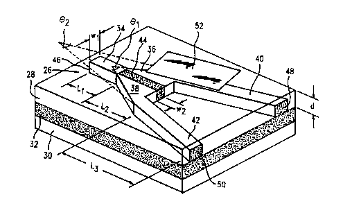
disclosure describes a Y-branch switch 26 which may be
grown on n-type: InP substrates. Upper cladding 28 and
lower cladding 30 may be p-type and n-type InP,
respectively, which may have thicknesses on the order of
about 1.0 Vim. The disclosed switch 26 includes an
active core 32 and waveguide portions 36-42 fabricated
as a waveguide layer structure grown by a metallorganic
~
~18318G
6
chemical vapor deposition (MOCVD) process (known in the
art) on the n-type InP substrate 28, with the active core
32 being about 0.55 ~Cm thick and having, for example,
about 30 quantum wells, which may be composed of
InGaAsP/InP. It is understood that one skilled in the
art may fabricate the quantum wells using other materials
and growth methods. It is also understood that one
skilled in the art may use other materials for the
cladding and substrate. Reactive ion etching with CH4/Ha
may be used to etch the waveguide portions 34-42 and an
electrical isolation groove or gap 44 in one step.
The disclosed switch 26 includes a first waveguide
portion 34, intermediate waveguide portions 36, 38, and
branch waveguide-portions 40, 42 fabricated-in a manner
substantially similar to the composition ofthe active
core 32. The first waveguide portion 34 includes an
input port region 46, and the branch waveguide portions
40, 42 include a respective output port region 48, 50.
In an exemplary embodiment, the waveguide width wl
of waveguide portions 34-42 maybe about 3.0 ~m and the
etch depth d may be about 1.65 Vim. The disclosed switch
26 may be planarized with polyimide, with access visa
etched on top of the waveguide portions 34-42, and Cr/Au
contact pads such as pad 52 may be evaporated on top of
respective waveguide portions 34-42. The disclosed
switch 26 may be mounted on Cu posts and terminated with
chip resistors of about 47 i1 (not shown in FIG. 2).
Aa described in M.nT. Khan et al., ~~Design and
Demonstration of Weighted-Coupling Digital Y-Branch
~ ;~18318~
7
Optical Switches in InGaAs/InGaAlAs Electron Transfer
Waveguidea", JbURNAL OF LIGHTTiVAVE TECHNOLOGY, VOL. 12,
NO. 11, November-1994, pp. 2032-2039;'and in M.N. Khan et
al., "Weighted-CouplingY-Branch Optical Switch in
InGaAS/InGaAlAs Quantum Well Electron Transfer
Waveguides", IEEE PHOTODTICS TECHNOLOGY LETTERS, VOL. 6,
NO. 3, March 1994, pp. 394-397, the taper angles 61 and
Aa and lengths of the waveguide portions 36-42 may be
optimized to improve performance of Y-branch switches.
In a preferred embodiment, the first waveguide
portion 34 may be substantially straight with a length L1
of about 100 ~Cm, and functions as a passive waveguide
section for receiving electromagnetic energy at an input
port
Each intermediate waveguide portion 36, 38 may have
a substantially triangular shape with a length L2 of
about 180 ~m and forming, with an region 44 therebetween,
a substantially trapezoidal shape associated with a first
taper angle 01 of about 1.8°. That is, rays parallel to
an associated surface of the trapezoidal shape define the
first taper angle 81 at their intersection, as shown in
FIG. 2. Each branch waveguide portion 40, 42 may be
substantially straight and have a length L3 of about 620
~m and an associated second taper angle 0a of about 0.2°;
i.e. rays parallel to. an associated surface of each
branch waveguide portion 40, 42 define the second taper
angle 0z at their Intersection, as shown in FIG. 2-.
The trapezoidal section has a first base where the
branch waveguide portions 40, 42 merge, and a second base
~18318~
8
tapers with the first taper angle A1. The trapezoidal -
section, including the intermediate waveguide portions
36, 38, functions as an active common v~aveguide section
for converting the received-electromagnetic energy from
the first waveguide portion 36 to optical energy at one
of a first and second refractive indexes. Each of the
branch waveguide portions 40, 42 is operatively connected
to a respective intermediate portion 36, 38 and is
arranged to receive the optical energy at the respective
first and second refractive indexes.
The disclosed switch 26 thus provides a relatively
compact Y-shaped adiabatic structure with a total length
LT~~, of about 900 Vim. It is understood that one skilled
in the art may implement the disclosed switch 26 with
waveguide portions 34-42 that are curved, where each of
waveguide portions 34-42 is configured and/or having
tangential surfaces forming angles substantially near the
taper angles 01 and 8z.
The electrical isolation gap 44 is positioned at the
vertex of the Y-branch between the intermediate waveguide
portions 36, 38, with the width wa of the gap 44 being
about 1.6 hem, which provides for relative ease in
fabrication of the disclosed switch 26. Such electrical
isolation may be achieved by either ion implantation or
etching. -- ,
The disclosed switch 26 with the exemplary
configuration described above provides for low crosstalk,
ease of fabrication, and low propagation lose. The
disclosed switch 26 has a reduced voltage-length product
~ G,1831~&
9
while providing fabrication tolerance-and a better
crosstalk performance at a shorter device length than
heretofore attained.
As described in M.N. Khan et al., "Design and
Demonstration of Weighted-Coupling Digital Y-Branch
Optical Switches in InGaAa/InGaAlAs Electron Transfer-
Waveguides", s~nra. at 2D35, crosstalk values are plotted
as a function of 'the taper angles 01 and 0" where the
first taper angle 01 may be in the range of about 1.5° to
about 2.0° to attain improved crosstalk performance. The
disclosed switch 26 as described above has a first taper
angle 81 for a sufficient taper of the branch waveguide
portions 40, 42 to be fabrication tolerant for
photolithography techniques-known in the art. The
relatively wide first taper angle 01 followed by the
relatively narrow second taper angle 02 maintains the
adiabaticity of-the disclosed switch 26.
In an exemplary embodiment, the disclosed switch 26
has a propagation loss of about 1.25 dB/mm and excess
lossesas low as about O.10 dB in 900 ~m long devices.
The disclosed switch 26 also provides for digital
switching characteristics with a crosstalk of about -25
dB for an active length of about 800 Vim, which may be
attained by providing an index change ~n of about 0.001
in one of branch waveguide portions 40, 42 with respect
to the other, with a radiation loss of about O.DS dB.
Such crosstalk values may be verified using beam
propagation methods (BPM) known in the art. Such an
index change is also fabrication tolerant since the
~ ~,~8318~~
1~
relatively wide first taper angle 01 allows the isolation
gap 44 in the Y-branch vertex to be relatively large. -
The disclosed switch 26 may also perform high-speed
switching operations by using a voltage-controlled
refractive index change, allowing for a 3 dB bandwidth of
about 10 GHz employing a switching voltage of about -4V.
The crosstalk performance may be further improved-by
simultaneously driving both arms with two different
negative DC biases to increase the differential index
change between the two ports. The signal modulation
response of the disclosed switch as a function of drive
frequency is shown in FIG. 3, which was measured using an
HP 8703 optical network analyzer. A 3 dB electrical
bandwidth of 10 GHz may then be attained by the disclosed
switch 26 to be the highest speed reported for a digital
switch. The measured data yields values of packaged
switch inductance L of about 0.6 nH and capacitance C of
about 0.32 pF, with contact series resistance R of about
46 L1. An exemplary voltage used for switching is less
than about -4V with a single branch waveguide portion of
the disclosed switch 26 being driven.
While the disclosed tapered Y-branch switch has been
particularly shown and described with reference to the
preferred embodiments, it is understood by those skilled
in the art that various modifications in form and detail
may be made therein without departing from the scope and
spirit ofthe invention. accordingly, modifications such
as those suggested above, but not limited thereto, are to
be considered within the scope of the invention.