Note: Descriptions are shown in the official language in which they were submitted.
CA 02183347 2000-10-27
WO 95/23997 PCT/GB95/00-l25
1
OPTICAL Al'VD GATE
BACKGROUND TO THE INVENTION
The present invention relates to an all-optical gate
far carrying out an AND logic operation. Such a gate a fight
be used, for example, in an optical telecommunications
system, or in optical data-processing devices.
AND is a fundamental logic operation necessary for
example, for the implementation of optical networks
including photonic switching nodes. Our co-pending
international application no. PCT/GB94/00397, describes
and claims one example of the use of an AND function in
recognising an address carried in the header of a frame
on the optical network, and controlling a routing switch
accordingly.
It has recently been proposed to use the process known
as four-wave mixing (FWM) to implement an AND function.
FWM produces an output proportional to the product of the
electric fields of two input optical signals. Andrekson et
al: "l6Gbit/s All Optical Demultiplexing Using Four-wave
Mixing," Electron. Lett., 27, 1991, pp.922 and R. Schnable,
W. Pieper, R. Ludwig, H.G. Weber: "All Optical AND Gate
using Femtosecond Non-linear Gain Dynamics in Semiconductor
Laser Amplifiers", ECOC '93 describe implementations of AND
functions using FWM in single-mode optical fibre and in
semiconductor laser amplifiers (SLAB) respectively.
Potentially such devices might be appropriate for switching
or logic processing functions in optical telecommunications
networks. However, the optical-fibre based devices require
long interaction lengths, and so have a large in-built
switch latency. This latency makes-such devices unsuitable
for applications where a fast decision time is required.
SLAB by contrast have short device lengths, and hence low
latency and are capable of high switching speeds due to
their non-linear gain dynamics.
WO 95/23997 PCT/GB95/00425
y ~:~ ;. 21 X3347
2
SUMMARY OF THE INVENTION
According to a first aspect of the present invention,
there is provided an optical AND gate including at least
one semiconductor laser amplifier (SLA) and inputs for
first and second optical signals (A, B), the AND gate being
arranged by a process of four wave mixing (FWM) to produce
an output corresponding to the AND product of the first and
second optical signals (A,B), characterised in that the
first and second optical signals are substantially equal in
wavelength.
Hitherto, optical AND gates using FWM have suffered
the serious limitation that they can only function
efficiently with signals which are at different frequencies
within a certain narrowly defined range. For example, the
above-cited paper by Andrekson et al requires a minimum
separation between the signals to be ANDed of .8nm and at
this separation suffers problems of crosstalk which make it
desirable in general to use an even greater wavelength
spacing. The present invention overcomes this limitation
to provide an AND gate which functions with wavelength-
degenerate inputs. These may, for example, be derived from
a common source and so have identical wavelengths, or may
be produced by different sources operating at a common
standard wavelength
Preferably the optical AND gate is further
characterised by an input for a third optical signal (P)
arranged, by interaction with at least one of the first and
second optical signals, to promote FWM within the at least
one SLA.
In this preferred aspect of the present invention, a
third optical signal, which may be a continuous wave
signal, and is at a different wavelength to the two
signals (A, B) is input to the AND gate and undergoes four-
wave mixing. This may interact, for example, by beating
with one of the two signals (A, B), and thereby causing
modulation of the carrier distribution within the SLA,
producing a dynamic grating. The other of the two signals
WO 95123997 PCT/GB95/00425
3 218~3~1
(A, B) then scatters off this dynamic grating generating
FWM sidebands.
Preferably the optical AND gate comprises a single SLA
arranged to receive the first signal and the third optical
' 5 signal, the first and third optical signals being co
polarised, and arranged to receive the second optical
signal in an orthogonal polarisation state to the first and
third optical signals, and means for selecting a sideband
output from the SLA corresponding to the AND product (C) of
the other optical signal with the one optical signal and
the third optical signal.
This aspect of the present invention uses signals in
orthogonal polarisation states to provide an AND gate based
on a single SLA. The interaction of a pair of co-polarised
optical signals in the SLA produces a modulation of the SLA
carrier densities distribution. This pair of co-polarised
optical signals comprises a pump signal P which is a
continuous wave signal, together with the first of the
signals to be ANDed, A. The other signal B is then
injected into the SLA in an orthogonal polarisation state.
Because of this orthogonality, FWM does not take place
between B and P alone or B and A alone. However, the
modulation of the carrier distribution in the SLA produces
effects which are non-polarisation sensitive, producing a
dynamic grating, as already described. The other signal B
scatters off the dynamic grating resulting in the
production of FWM sidebands in the output from the SLA.
With an appropriate filter, one of the sidebands can be
selected to provide an output corresponding to the AND
~30 function between A and B.
Preferably the optical AND gate includes a polarising
beam-splitter/combiner on the input side of the SLA for
receiving the orthogonally polarised signal (B).
The above-described AND gate with an orthogonally
' 35 polarised input is not limited to use with wavelength
degenerate inputs. Where such an AND gate is used in place
of a conventional AND gate to process signals at different
WO 95/23997 PCT/GB95100425
21833~~
4
wavelengths, it offers the advantage that its efficiency is
less dependent upon the magnitude of the wavelength-spacing
between the inputs, by comparison with conventional
devices.
According to a second aspect of the present invention
there is provided an optical AND gate including a
semiconductor laser amplifier (SLA) having inputs for
first, second and third optical signals, the first and
third optical signals (A, P) being co-polarised and
interacting in the SLA by a process of four-wave mixing
(FWM), and means for selecting an FWM sideband output from
the SLA, characterised in that the input for the second
optical signal is arranged to receive that signal
orthogonally polarised with respect to the first and second
optical signals, the first and third optical signals
beating and thereby generating a dynamic grating,
interaction of the second optical signal with the dynamic
grating producing the FWM sideband corresponding to the AND
product of the orthogonally polarised second optical signal
with the first and second optical signals.
As an alternative to the use of a single SLA with an
orthogonally polarised input, the optical AND gate may
comprise a first SLA arranged to receive the first optical
signal (A) together with the third signal (P) at a
different wavelength to the first optical signal, means for
selecting a sideband output from the first SLA, a second
SLA arranged to receive the selected sideband output from
the first SLA together with the second optical signal (B),
and means for selecting a sideband in the output of the
second SLA corresponding to the AND product (C) of the said
first and second signals (A, B).
According to a third aspect of the present invention
a method of ANDing two optical signals comprising applying
first and second optical signals (A, B) to an optical AND
gate comprising at least one semiconductor laser amplifier
(SLA) and by a process of four-wave mixing producing an
output from the at least one SLA corresponding to the AND
WO 95123997 PCT/GB95/00425
_ ~, y ~.
2183347
product of the first and second optical signals is
characterised in that the first and second optical signals
are substantially equal in wavelength.
According to a fourth aspect of the present invention
5 there is provided a method of ANDing optical signals
comprising inputting first and second optical signals, and
a third optical signal co-polarised with respect to the
first optical signal, to an optical AND gate, applying the
first and third optical signals to a semiconductor laser
amplifier (SLA), generating four-wave mixing (FWM) in the
SLA, and selecting a sideband in the output from the SLA
corresponding to the AND product, characterised by applying
the second optical signal to the SLA orthogonally polarised
with respect to the first and third optical signals, the
selected sideband corresponding to the AND product of the
second orthogonally polarised optical signal with the first
and second optical signals.
The present invention also encompasses a method and
apparatus for demultiplexing using the optical gates of the
first and second aspects.
BRIEF DESCRIPTION OF THE DRAWINGS
Systems embodying the present invention will now be
further described, by way of example only, with reference
to the accompanying drawings in which:
Figure 1 is a schematic of a first embodiment;
Figure 2 shows the output spectrum of the SLA of
Figure 1 after the polarises, with RZ data and the
polarises set in B polarisation plane;
Figure 3 shows oscilloscope traces for signals A, B,
and AND at the output of the final filter;
Figure 4 shows a comparison of input pulse width with
the output AND signal;
Figure 5 is a schematic of a PLL using the AND gate of
Figure 1;
Figure 6a to 6d illustrate the use of the AND gate for
NRZ to RZ conversions;
WO 95/23997 PCT/GB95/00425
:~ .~ : :-: ~ ,.. 218 3 3 ~ 7
6
Figure 7 is a schematic of a first example of an SLA
for use in the circuit of Figure 1;
Figure a is a schematic of a second example of an SLA
for use in the circuit of Figure 1;
Figure 9 shows the output spectrum of the SLA of
Figure 1 after the polariser when A and B are at 1546nm
using NRZ data;
Figure 10 is a plot illustrating bit-error ratio (BER)
achieved for NRZ data at -2.5Gbit/s;
Figure 11 is a schematic illustrating the output of
the system of Figure 1 when signals B and A are at
different optical frequencies;
Figure 12 is a schematic of a second embodiment
employing two SLAB;
Figure 13 shows an integrated planar circuit
implementation of the circuit of Figure 1 on InP/InGaAsP;
Figures 14a and 14b show the signal source and signal
receiver used in a demonstration of the circuit of Figure
1 at lOGbit/s;
Figure 15 shows oscilloscope traces obtained at
lOGbit/s;
Figure 16 shows output spectra in B polarisation plane
obtained at lOGbit/s;
Figure 17 shows bit-error-ratios at lOGbit/s;
Figure 18 shows bit-error-ratios at lOGbit/s measured
using a modified circuit;
Figure 19 is an oscilloscope trace showing the output
of the circuit at lOGbit/s;
Figure 20 is a graph showing correlation profiles; and
Figure 21 is a demultiplexer incorporating an AND gate
embodying the present invention.
DESCRIPTION OF EXAMPLES
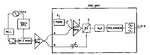
An optical AND gate includes a semiconductor laser
amplifier (SLA) 1 and inputs for a first optical signal A
and a second optical signal B. A source 2 generates a
third optical signal P. The first optical signal A is
WO 95!23997 PCT/GB95/00425
218~~~7
7
combined with the third signal P in an optical coupler, and
fed to a fibre amplifier 4. In this example, the fibre
amplifier is an erbium-doped device.
The second optical signal B is combined with the
output of the fibre amplifier using a polarising beam
splitter/combiner 5. The combined signals are then input
to the SLA 1. The output from the SLA is then passed
through a polarisation analyser 6 and bandpass filter 7 to
provide the output from the AND gate.
In this first example, the SLA is a strained-layer S-
well MQW (multiple quantum-well) buried heterostructure
device (Figure 7). It is 1000~.m long and 200 ~Cm wide and
has a gain peak in the region of 1.56~m when biased at
340mA. The active region has a width w of 1.2~,m. It
comprises alternate layers of Ino.53Gao.arAs 40A deep and
Ino.3~Gao.~As 60A deep. These quantum wells are bounded
between upper and lower layers of InGaAsP 500A deep. Using
this device, the results shown in Figures 2, 3 and 4 were
obtained.
Figure 8 shows an alternative bulk SLA which might be
used in the circuit of Figure 1. Here the device is 500~m
long and 200 ~m wide has an active region with a width w of
1.17~m. An InP core 0.23~.m deep is confined between an
upper layer Q~.~ 0.21~,m deep and a lower layer Q~.59 0.2~m
deep.
The third of the input signals, P, the pump signal, is
a continuous wave signal derived from a tunable external-
cavity semiconductor laser such as model no. Intun 1500
manufactured by Radians Innova. It operates in this
example at a wavelength of 1555.08nm. The second signal A
is at a wavelength of 1553.15nm and is combined with the
first signal in the coupler 3 which may be a 3dB fused
fibre coupler. The polarisations of A, B and P are
optimised for maximum transmission through the polarising
beam splitter 5, which may be a SIFAM high birefingence
fibre polarization beamsplitter. The beamsplitter ensures
that B is orthogonal to A and P.
WO 95/23997 PCT/GB95/00425
2183347 _
8
The output from the SLA is passed through the
polarising filter which in this example is a fibre
polariser adjusted to extinguish the signals in the A+P
polarisation plane. This is followed by a 0.6nm fibre-
s grating bandpass filter centred at 1551.20nm. As will be
further described below, this serves to isolate the AND
signal. A delay line is provided in the input path for the
second signal 13 to the beam splitter 5.
For convenience, in the example shown in the Figure
the inputs A and B are generated from a common source. In
practice the input at A might typically be provided, for
example, by the header of a packet carried on an optical
network and B might be a target word to be ANDed with the
header for the purposes of header recognition, as described
in our above cited co-pending international application.
In the circuit shown in Figure 1, the source for A and
B is an external cavity semiconductor laser (MLL)
fundamentally mode-locked at 3GHz using an amplified
electrical signal from a synthesised microwave generator.
The output pulses from the mode-locked laser are -0.2nm in
spectral width and of -20ps duration as measured on a
streak camera. The microwave generator is also used to
synchronise a pulse-pattern generator PPG which in turn
drives a Lithium Niobate Mach-Zehnder modulator. The
optical pulses from the mode-locked laser are amplified and
passed through the M-Z modulator. The resulting pulse
pattern is then amplified again and split between signal
paths A and B using a fused fibre coupler. There is a
length difference (time delay) between paths A and B, which
can be fine-tuned using a variable length fibre delay line
to synchronise bit arrivals in the SLA.
In use, a 16-bit optical sequence of pulses was
generated to demonstrate the AND function. The optical
power levels measured at the input to the SLA were +9dBm
for A + P in combination and -ldBm for signal B. The pump
is of a high enough power to prevent modulation of the SLA
spontaneous emission by A and B. The ratio of A to P is
WO 95/23997 PCT/GB95/00425
2183347
9
-lldB as measured on an optical spectrum analyser. The
optical spectrum measured at the output of the polarises
. (set for B polarisation plane) is shown in Figure 2 for
combinations of A on/off and B on/off. The AND signal is
indicated. This signal is produced as an FWM sideband
generated from the orthogonally polarised signal B in the
presence of the modulation of the carrier density
distribution resulting from the beating between the pump P
and the signal A. This AND signal is entirely extinguished
when A or B is absent. The small average power level of
the AND signal in the trace is largely due to the small
number of is in the AND pattern.
Figure 9 shows the output of the AND gate when the
input signals A and B are NRZ-modulated at a wavelength of
1546nm. As in the first example above, a strong AND signal
is produced at a wavelength in the region of 1544nm and can
be selected by an appropriately tuned filter.
Although in these examples A and B are at a single
common wavelength, the invention is by no means limited to
operation in this fashion. Figure 11 shows schematically
the expected form of the output when A and B are at
different optical frequencies. At the output, A and P can
be selected out using a polarising filter as described
above and then one of the sidebands of B corresponding to
the AND product is selected with an appropriately tuned
bandpass filter.
Figure 3 shows the normalised traces from a photodiode
used to detect the output from the gate, as captured on a
sampling oscilloscope . The top trace shows the pulse train
A at the output of the final filter with the filter and
polarises adjusted to isolate A. The middle trace of
Figure 3 shows the same for the B signal, but with the
polarises adjusted to show B. The bottom trace shows the
output of the AND gate resulting from the above input data
sequences. The AND gate can be seen to give a pulse only
when pulses from both A and B are coincident in the SLA.
WO 95/23997 PCT/GB95100425
218347
The pulse shape for signal A is compared with the AND
signal pulse shape in Figure 4. There is no pulse
broadening, thus demonstrating the ultrafast operating
speed of the AND gate. The width of the AND pulse is
5 narrower than the input pulse due to the correlation
between A and B in the SLA.
The device is found to be remarkably stable in
operation. The polarising beam splitter ensures
orthogonality of the A + P and B signals so the most
10 critical adjustment is to the polariser as this determines
the extinction ratio. The device can be improved by using
polarisation maintaining ffibre on either side of the SLA.
In the plot shown in Figure 10, an AND signal BER
(bit-error-ratio) is obtained by delaying the first input
A relative to B by one complete pattern length. Therefore
in the AND gate the pattern is combined with a delayed
version of itself. The AND signal is therefore the
original pattern. The second plot on the graph shows the
output "back-to-back" without the AND gate in place to
determine the baseline receiver sensitivity.
For prototyping and testing, it is convenient to
construct the circuits described above using discrete
components which are commercially available with fibre
pigtails, thus allowing rapid and relatively simple
construction by splicing or using fibre connectors. The
use of components joined with fibre connectors facilitates
the measurement of key parameters at critical points in the
device, such as at the SLA input port. In commercial
realisations of the circuit however it may be advantageous
to form the circuit as an integrated device. This serves
both to reduce manufacturing costs, to reduce the space
taken by the circuit, and to increase the reliability of
the circuit. Performance may also be improved by the
elimination of fibre coupling losses.
Figure 13 shows an integrated implementation of the
circuit of Figure 1, in which signal A combines with a co-
polarised pump signal, which is produced by a high power
WO 95/23997 PCT/GB95/00425
Sl i ;. i
11
DFB laser 130 fabricated on the chip, in a directional
coupler 131. This may be fabricated using conventional
photolithographic and epitaxial techniques on Indium
Phosphide using an Indium Gallium Arsenide Phosphide active
region and waveguide layers. The combined signal is then
coupled with the B signal in a polarisation coupler 132
before entering an integrated SLA. At the output of the
SLA is an optical filter 133 with a grating designed to
pass signals at the wavelength corresponding to the AND
sideband. Finally, the filtered signal is passed through
another polarisation coupler 134 to remove the remaining
unwanted signals and is detected on a photodiode. Other
photodiodes are included on the chip to monitor the circuit
and to provide data for element management. Optionally,
additional SLAs might be integrated on the chip to amplify
the signals. These however may distort ultra-short optical
pulses so it may be preferable to use external EDFAs
(erbium-doped fibre amplifiers) where application is
desired. As a further alternative, a hybrid planar
structure might be used with erbium-doped silica waveguides
integrated with the circuit on a silicon substrate.
Figures 14a and 14b show a modified signal source, and
signal receiver respectively used in demonstrating the
operation of the circuit of Figure 1 at a bit-rate of
lOGbit/s.
Light from CW DFB laser 140 at 1551.24 nm is passed
through a 60 dB optical isolator 141 and coupled into an
EAM 142 (electroabsorption modulator) with a modulation
bandwidth in excess of lOGHz. A 9.8174Gbit/s electrical
PRBS of 27-1 bit-length from a Hewlett Packard lOGbit/s PPG
143 is amplified by a wideband amplifier and applied to the
EAM via a bias T. The resultant intensity-modulated
optical output is then amplified by an EDFA to an average
optical power level of about +lOdBm. This amplified
optical signal is then ffiltered by a tunable filter with a
l.2nm pass-band to remove excess spontaneous emission from
the EDFA. The signal is then split using a lOdB coupler
WO 95/23997 PCT/GB95/00425
v
21 a~341
12
144 such that signal A incurs an extra lOdB loss relative
to signal B. The two signals then enter the AND gate via
two optical attenuators. The AND circuit was constructed
as previously described with reference to Figure 1, but
with some minor modifications. The polarisation combiner
was changed to a JDS polarising beam splitter with a lower
insertion loss. As this combiner did not have a fourth
port through which the coupled power could be monitored, a
fused fibre coupler is placed between it and the SLA as a
lOdB power tap. The SLA is a bulk active layer device as
described above with respect to Figure 8. This bulk layer
device has been found to offer more efficient FWM than, for
example, the MQW SLA of Figure 7.
The output from the AND gate is detected by the
optically pre-amplified receiver shown in Figure 14b. This
consists of an EDFA followed by a tunable optical filter
145 with a lnm pass-band and a lSGHz Hewlett Packard light
wave convertor 146. The electrical output from the light
wave convertor was then fed into either an error detector
147 or to a digitising oscilloscope.
Using the circuit, measurements were taken to verify
that the gate was performing the required AND function at
lOGbit/s. The A and B signals at optical power levels of
+ 8.2dBm and + 2.7dBm respectively were injected into the
SLA biased at 310mA. The wavelength of the pump beam P was
set at 1553.8nm and at an optical power of +9.8dBm. The
EAM was biased at - 3V and slightly overdriven by the data
signal to ensure that the 1 states do~ not extend beyond the
allocated 100ps time slot. This measure was necessary to
ensure that when a 10 pattern and a O1 pattern from inputs
A and B arrived at the AND gate simultaneously, the wings
of the is did not overlap causing an AND output signal that
appeared like poor extinction. This driving condition was
not necessary when taking error ratio measurements as the
bit overlap was outside the sampling window, but here it
aided the interpretation of the results. A short sequence
from the AND, A and B data patterns at the output of the
WO 95/23997 PCT/GB95/00425
21 ~~3~-7
13
AND gate was captured on the oscilloscope by proper
adjustment of the filters and polarisation of the SLA. The
- resulting traces are shown in Figure 15. Figure 16 shows
the optical spectra obtained at the output of the polariser
prior to filtering and demonstrate an excellent extinction
ratio better than 20dH. Figure 17 shows the results of
measurements of the BER at lOGbit/s. This measurement was
made with the SLA biased at 285mA and slightly cooled to
14°C, as this seemed to improve FWM efficiency. The
l0 optical power levels at the input to the SLA were + 6.4dBm,
+ 2.8dBm and +10.8dBm for A, B and P respectively. The
bias voltage on the EAM was reduced to 1.8V to lower the
insertion loss of the modulator and improve the system
performance.
Further measurements were made with a lOGHz bandwidth
pre-amplifier added after the light wave convertor to band-
limit the pulses entering the error-rate detector. A 600m
length of dispersion-compensating fibre was inserted in the
input B path to enable longer patterns to overlap at the
input to the AND gate. The EAM transmitter was biased at
-3V and driven by a lOGbit/s 2'3-1 PRHS. The exact bit-rate
was changed by 384kHz to give either exactly overlapped
patterns at the AND gate input or patterns delayed by one-
bit. The wavelength of the source DFB was 1551.2nm and P
was 1553.3nm. The power levels measured at the input to
the SLA were -O.ldBm, +l.OdBm and +7.8dBm for A, B and P
respectively. The SLA was biased at 291mA and maintained
at a temperature of 15°C. Figure 18 shows the BER results
obtained in this example, and Figure 19 shows an
oscilloscope recording of the AND signal output.
With the AND gate operating as described in the
immediately proceeding paragraphs, correlation measurements
were made to demonstrate that the response of the AND gate
is sufficient to handle 100Gbit/s data pulses. A first
measurement was made by adjusting the input signal
repetition rate so as to cause the relative arrival times
of pulses at the A and B inputs of the AND gate to vary
WO 95/23997 PCT/GB95100425
~., ~ , ~ _ . ~ , 218 3 3 ~ 7
...
14
linearly. This allowed one stream of pulses to pass
through the other and perform a cross-correlation between
the two pulse streams. Measurements were also made with a
commercial autocorrelator on the output of the AND gate.
The source signal was provided by a CWDFB laser at 1551nm
injected into a lOGHz bandwidth EAM.
Figure 20 shows the results obtained. The half width
measured using cross-correlation in the AND gate was
10.7ps, and the half width of the trace from the
autocorrelator was 11.6ps. If the pulse profile is assumed
to be in the form of a sechz function, then the actual
pulse width is a factor of 1.55 less than the correlation
width, giving a value of 7ps. This value for the pulse
width demonstrates the AND gate can operate at data rates
in excess of 100Gbit/s.
Figure 12 shows another embodiment using two SLAB
connected in series. A continuous wave pump, which may be
generated as described above, is input to SLA 1 together
with signal A. The filtered output from SLA 1 is then
input to SLA 2 together with the second optical signal B.
In the first SLA, a non-degenerate four-wave mixing process
between the signal A and the pump generates an optical
signal at a new wavelength APC given by CPC=~P~s/ (2~s-~P) «a
is the wavelength of the pump and ~s the wavelength of the
signals A and B). The new signal at CPC is selected at the
output of the SLA using a first bandpass filter BPF1. Non-
degenerate four-wave mixing of the output from the first
SLA together with signal B in the second SLA generates a
further optical signal at another new wavelength ~ given
by ~c=~s~'ac~ ~2wc-~s) ~ This signal is selected using a second
bandpass filter BPF2 to produce the signal C which can
occur only if the signals at A and B are present
simultaneously, i.e. it corresponds to the AND product of
A and B. This embodiment offers the advantage of avoiding
the need for polarisation control of the signals if
implemented using polarisation-independent FWM in each of
the SLA's. It is therefore particularly suitable for use
WO 95123997 PCT/GB95/00425
2 ~ ~3~~.1
at high bit rates at which polarisation presents particular
difficulties.
- Each of the two SLAB may be a discrete device and may
comprise, for example, an MQW semiconductor laser amplifier
5 as described with respect to Figure 7. The SLAB may be
connected to their respective inputs and to each other by
monomode optical fibre. The bandpass filters may
conveniently be formed as fibre gratings.
Alternatively, the two SLAB may be formed, together
10 with the filters, as a single integrated device.
An optical AND gate as described above may be used in
an optical telecommunications system for header
recognition. For a fuller description of this use of the
device reference is made to our co-pending international
15 application PCT/GB94/00397.
Another example of a field of use for the AND gate is
in an optical phase-locked loop. Such a loop may be used,
for example, in recovering a clock at a sub-multiple of the
clock rate of an input datastream. Figure 5 shows
schematically a circuit appropriate for this. The output
of the AND gate 51, which is constructed as in the example
above, passes to a photoelectric detector 52. The
electrical output from the detector is filtered by a low-
pass filter 53 and then used to control an optical voltage-
controlled oscillator 54 which generates the output optical
clock stream. This optical VCO may comprise a fibre ring-
cavity mode-locked laser incorporating a fibre-stretcher
e.g. a piezo-electric drum which ~is controlled by the
signal from the low-pass filter. A suitable laser is
described in our co-pending application PCT/GB94/00863.
This clock stream together with the original datastream
provide the two inputs of the AND gate 51 (equivalent to
signals A and B in the example above) . The AND gate 51
therefore functions as the phase-detector for the loop.
As well as such use of the gate for clock recovery, it
may be used for signal regeneration, or, for example, for
modulating an RZ (return to zero) clock with an NRZ
WO 95123997 PCT/GB95/00425
~ ;~ ., ;.
283347
~' '. ~., ~.::s = i~.
16
datastream. Figure 6a illustrates this with Figure 6b
showing the NRZ datastream, 6c the RZ clock, and 6d the
output pulse sequence.
A further important field of use for AND gates
embodying the present invention, is in demultiplexing
optical pulse streams which may take the form, for example,
of OTDM frames. Figure 21 is a schematic of an all-optical
demultiplexer using the AND gate of the present invention.
In this implementation, instead of using a polarising
l0 filter to extinguish the A and P signals, a polarisation
splitter is used on the output of the SLA. This separates
the AND sideband output at ~f~ to provide the demultiplexed
output, and transmits on the signal which is orthogonally
polarised with respect to the AND output. The fact that
the unswitched channels are still accessible is a
significant advantage of this demultiplexer. Such a
demultiplexer is well-suited to demultiplexing in a linear
bus configuration where the channels are to be dropped at
geographically separated nodes in a network. It is however
less suitable for use in a "drop and insert" node, as the
through signal has a significant proportion of the switched
channel remaining.
Polarisation insensitivity is important in
demultiplexing, as polarisation tends to wander with
temperature and stress variation in the transmission fibre.
The polarisation sensitivity of the AND gate of the present
invention might be eliminated either by reconfiguring the
device, and in particular by using the two-SLA form of the
AND gate, or by the use of fast automatic polarisation
controllers as described in F. Heismann et al
"Polarisation-independent photonic switching system using
fast automatic polarisation controllers" IEEE Photonics
Technology Letters Vol. 5 No. 11, 1993, on the input that
can compensate for polarisation variations in the
transmission fibre.