Note: Descriptions are shown in the official language in which they were submitted.
WO 96/19091 2 18 3 4 ~ 2 PCT/GB95/02947
COMMUNICATION S~ ~;S
This invention relates to communication switches for use in
communication systems to switch connections between respective
input and output ports for the transfer of data therebetween.
A known type of communication switch, commonly called a "matrix
switch", is used to connect any one of multiple input ports to
any one of multiple output ports. Matrix switches can be used
locally to interconnect local input and output ports, or
centrally to inter-connect input and output ports of remotely
located devices. For example, when port cards are interconnected
in a communication system, a central matrix switch card is
provided having the required level of connectivity for the total
number of card input ports and card output ports. This creates
a problem with expandable co~ml~n;cation systems in that, even
though the system may initially only incorporate a limited number
of port card options, the same central matrix switch card with
the maximum potential connectivity is still used. This makes
the initial installation cost disproportionately high.
An object of the present invention is to provide a communication
switch in which this problem is overcome or reduced.
This is achieved according to the invention by distributing the
central matrix switch between the port cards so that the
connectivity of the switch increases as additional port cards are
wog6/1sosl 21 8 3 ~ 4 2 pcTlGs95lo2947
added.
In particular, the invention consists in a communication switch
comprising a matrix of switch modules interconnected to allow
switching between multiple inputs and multiple outputs,
characterised in that said switch modules are distributed between
multiple input/output port cards so that each card incorporates
one or more switch modules with multiple outputs connected to
respective output ports of the card and multiple inputs connected
to respective transfer terminals of the card, the inputs of the
cards being interconnected via a set of buses connected to said
transfer terminals, and a selector being incorporated in each
card which is setable to connect each of one or more respective
input ports of the card to a selected input of said switch
modules on the same card, so that each input port of the switch
is uniquely connected via a respective selector to respective
input of a switch module and a respective bus.
The total number of input ports on all the cards equals the total
number of buses employed to give a non-blocking communication
switch. It is preferred that each switch module comprises a
square matrix switch with the same number of inputs and outputs.
An input/output port card used according to the invention may
comprise just one set of matrix switch modules connected in
series with just one set of output ports, and a corresponding set
of input ports. However, the switching capacity of a
communication switch can be increased by providing multiple sets
WO96/19091 218 3~ A 2 PCT/GB95/02947
of switch modules on a card, each set of the multiple set being
connected in series with a corresponding set of output ports, and
the inputs of these multiple sets of switch modules being
connected in parallel with the transfer terminals so that a
signal at any transfer terminal can be switched to any one of the
output ports. The multiple sets of output ports are then
matched by multiple sets of input ports, equal in number to the
sets of output ports, with each set of input ports being
connected via the selector to the corresponding transfer
term; n~l s, thereby to the inputs of the corresponding switch
module in each set of switch modules. An appropriate number
of buses are then provided to interconnect the multiple sets of
input ports and multiple sets of output ports with those of other
cards in a non-blocking communication switch. Thus different
switch modules may have different numbers of input ports and
output ports.
The number of switch modules incorporated in each set of switch
modules in a communication switch will be equal to the number of
sets of switch modules used in the system.
According to another feature of the invention, the input/output
port cards are incorporated in units that are stacked one on top
of another vertically, with electrical interconnections provided
between their cooperating surfaces.
The invention will now be described by way of example with
reference to the accompanying drawings in which:
WO96/19091 2 1 8 3 ~ ~ 2 PCT/GB95102947
Fiqure l is a schematic drawing of a communication system
according to a first embodiment of the invention;
Fiqure 2 is a schematic drawing of the mounting arrangement of
the output cards in the system of Figure l;
Fiqure 3 is a schematic drawing of a communication system
according to a second embodiment of the invention; and
Fiqure 4 is a schematic drawing showing a modification to the
communication system of Figures l or 3.
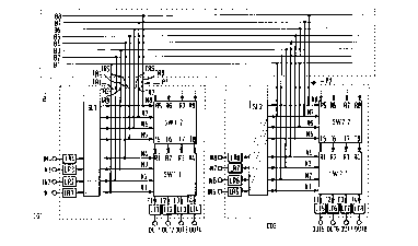
The illustrated communication system carries information in an
ATM cell format and comprises two communication switch cards CDl
and CD2, each with four input ports INl to IN4 and IN5 to IN8,
respectively, and four output ports OUTl to OUT4 and OUT5 to
OUT8, respectively. These two cards are interconnected via a
backplane B having eight buses Bl to B8 to which each card is
connected via eight transfer terminals TRl to TR8.
Each card CDl and CD2 incorporates two matrix switch modules
SWl.l and SWl.2 and SW2.l and SW2.2, respectively, each of these
modules SW being a square matrix switch having four inputs Nl to
N4 or N5 to N8 and four outputs Tl to T4 or T5 to T8. The two
modules SW on each card have their outputs connected in series
by interconnections between the outputs T5 to T8 of one module
SWl.2 or SW2.2 and interconnection terminals Rl to R4 of the
other module SWl.l or SW2.l so that each pair of modules forms
2183~2
_ WO96/19091 PCT/GB95/02947
a combined matrix switch with eight inputs Nl to N8 and four
outputs Tl to T4. Input signals on any one of the inputs Nl to
N8 can then be switched to any one of the outputs Tl to T4
according to routing information incorporated in the routing tags
of the ATM cells as further described below.
The four outputs Tl to T4 of the second series connected module
SWl.l or SW2.1 are connected via four respective line
transmitters LTl to LT4 or LT5 to LT8 to the four output ports
OUTl to OUT4 or OUT5 to OUT8 of the respective card. The eight
inputs Nl to N8 of each pair of modules SWl.l, SWl.2 and SW2.1,
SW2.2 are each connected to a respective one of the buses Bl to
B8 via a connector Pl or P2 comprising eight transfer terminals
TRl to TR8 on the card CDl or CD2. The four input ports INl to
IN4 or IN5 to IN8 are connected via four respective line
receivers LRl to LR4 or LR5 to LR8 and a selector SLl or SL2 to
the four inputs Nl to N4 or N5 to N8 of one of the modules SW as
determined by the setting of the selector SLl, SL2 so that the
four inputs INl to IN4 of one card CDl are connected to the
inputs Nl to N4 of the second module SWl.l in series on that
card, and the four inputs IN5 to IN8 of the other card CD2 are
connected to the inputs N5 to N8 of the first module SW2.2 in
series on that card. Each set of four input ports INl to IN4
or IN5 to IN8 is therefore also connected via the connector Pl
- or P2 to a respective set of buses Bl to B4 or B5 to B8 in the
backplane B.
In the operation of the system, any data received at an input
WO96/19091 2 ~ 8 3 4 ~ 2 PCT/GB95/02947
port INl to IN8 is processed by the respective line receiver LRl
to LR8 which generates the routing tag by which this data is to
be routed through the system to the corresponding output port
OUT1 to OUT8. The input data is then transmitted via the
selector SLl or SL2 to that input Nl to N8 of the modules SW1.1,
SWl.2 and SW2.1, SW2.2 to which that particular input port INl
to IN8 is connected. The input data is also transmitted to the
corresponding bus B1 to B8 to which this input Nl to N8 is
connected. For example, a data input at input port INl is
applied via the selector SL1 to the input N1 of the module SW1.1
and to the bus Bl.
Each of the switch modules SW operates to analyze the ATM cells
applied to its inputs Nl to N4 or N5 to N8 and reads the routing
tag of every ATM cell to determine whether that cell is intended
for one of the output ports OUT1 to OUT4 or OUT5 to OUT8 to which
the module is connected. If this condition applies, then the
cell is transmitted by the module SW to the appropriate output
port OUT1 to OUT8 via a respective line transmitter LTl to LT8
which removes the routing tag. Thus, if data is to be
transmitted between the input ports and output ports of the same
card CDl or CD2, then the route switching occurs in a switch
module SW of that same card, but if the data is to be transmitted
between the input port of one card CDl or CD2 and an output port
of the other card CD2 or CDl, then the route switching occurs in
a switch module SW of that other card after transmission of the
data on the corresponding bus Bl to B8 connecting said input port
to the switch module of said other card.
2183~42
WO96/19091 PCT/GB95/02947
The routing tag employed may, for example, comprise a plurality
of subfields, each corresponding to a particular card CDl or CD2
in the system, and each comprising a code that identifies one or
more of the possible four output ports OUTl to OUT4 or OUT5 to
OUT8. It will be appreciated that a cell can be transmitted
to any or all of the output ports OUTl to OUT8 by the use of
appropriate output codes.
An example of a suitable matrix switch module SW for use in the
illustrated embodiment of the invention is the Fujitsu MB86680B
ATM Switch Element.
A conventional physical arrangement of the cards CDl, CD2 of a
system would involve mounting the cards upright in a rack with
the connectors Pl, P2 at the rear edge between the cards and an
upright motherboard that incorporates the backplane. An
alternative arrangement, however, is illustrated in Figure 2 in
which the cards CDl, CD2 are stacked one on top of another. The
bottom card CDl is the first, and in some systems may be the only
card that is required, and thus it is supplied in a housing unit
H with other system requirements, such as a power supply PSU, a
management control card CDM and a fan tray FT. The other cards
CD2, CD3 etc. do not include the management control card CDM or
power supply unit PSU, but each is mounted in a housing unit H
and is provided with a fan tray FT. The connectors Pl, P2
between cards CDl, CD2, CD3, etc, are provided as cooperating two
part connectors that engage automatically as the cards are
stacked.
21 ~44 7
WO96/19091 PCT/GB95/02947
The buses Bl to B8 may, for example, each comprise a multi-
conductor parallel bus having eight conductors carrying data, one
carrying a synchronisation signal, and one carrying a clock
signal.
The setting of the selectors SL1, SL2 to make the appropriate
unique connections between the input ports INl to IN4 and IN5 to
IN8 can be predetermined by the connectors P1, P2, the engagement
of a connector when plugging in a card CD1, CD2 to a socket in
the backplane B serving to set the selector SL1, SL2 in the
appropriate manner. Alternatively, the system may include a
control unit which identifies those connectors P1, P2 that have
been made and those that have not been made, and sets the
selectors SL1, SL2 accordingly.
It will be appreciated that the illustrated system can be readily
expanded to incorporate three or more cards by increasing the
number of buses in the backplane B so as to accommodate the extra
interconnections required between cards for the extra input ports
and output ports. At the same time, the number of matrix switch
modules SW connected in series on each card will have to be
increased so that the combined matrix switch still has a separate
input for every bus. Thus, the addition of a third card in the
illustrated system would require each card to have a third switch
module with four inputs for the four extra buses and with the
four outputs connected in series to the interconnection terminals
R5 to R8 of the second modules SW1.2 and SW2.2 as shown in broken
outline in Figure 1. Thus, in this example, the number of
2I83~A~
WO96/19091 PCT/GB95/02947
modules on each card equals the number of cards in the system,
and the total number of modules equals the square of the number
of cards.
An alternative embodiment of the invention is illustrated in
Figure 3 comprising two communication switch cards CDl and CD2,
one of which CDl incorporates a set of three matrix switch
modules SWl.l, SWl.2, SWl. 3 connected in series with a set of
output ports OUTl to OUT4 in the manner of the card CDl
illustrated in Figure 1, and the other of which CD2 incorporates
two sets of three matrix switch modules SW2.2, SW2.2, SW2. 3 and
SW2.4, SW2.5, SW2. 6 each connected in series with a set of output
ports OUT5 to OUT8 and OUT9 to OUT12 in the manner of the set of
switch modules SWl.l, SWl. 2, SWl. 3 of card CDl. As shown in
Figure 3, each set of output ports OUTl to OUT4, OUT5 to OUT8 and
OUT9 to OUT12 are shown as a broad line for reasons of simplicity
in the drawing, and it will be appreciated that each such broad
line represents a set of four connections, ports or terminals.
Thus, the card CDl has four input ports INl to IN4 connected via
the selector SLl to four inputs of the third switch module SWl.l,
and each switch module SWl.l, SWl.2, SWl.3 has a set of four
inputs connected via respective sets of transfer terminals TRl
to TR4, TR5 to TR8, TR9 to TR12 to respective sets of buses Bl
to B4, B5 to B8, B9 to B12.
The card CD2 has two sets of four input ports IN5 to IN8 and IN9
to IN12, each connected via a selector SL2 to the inputs IN5 to
IN8 of the second switch module SW2.2 and inputs IN9 to IN12 of
2183'~42
WO96/19091 PCT/GB95/02947
the first switch module SW2.3, respectively. Also, each set of
four inputs of each switch module SW2.1, SW2.2, SW2.3 is
connected via respective sets of transfer terminals TRl to TR4,
TR5 to TR8, TR9 to TR12 to respective buses Bl to B4, B5 to B8,
B9 to B12. Furthermore, each set of four inputs of the second
set of switch modules SW2.4, SW2.5, SW2.6 is connected in
parallel with the corresponding inputs of the respective switch
modules SW2.1, SW2.2, SW2.3 of the first set, this being achieved
using a set of four regeneration outputs RGl to RG4, RG5 to RG8,
RG9 to RG12 of the switch modules of the first set. Thus, card
CD2 has eight input ports IN5 to IN12 and eight output ports OUT5
to OUT12 compared with the four input ports INl to IN4 and output
ports OUTl to OUT4 of the card CDl.
The communication switch cards CDl, CD2 of either Figure 1 or
Figure 3 can be modified as shown in Figure 4 so that two or more
input signals are multiplexed at each input port and de-
multiplexed into separate output signals at each output port,
thereby effectively increasing the number of input and output
ports within the maximum bit rate limit of each input port and
output port. As shown in Figure 4, each input port INl to IN4
and output port OUTl to OUT4 is divided into a pair of ports,
which are combined with a multiplexer MXl to MX4 at the inputs
or demultiplexed by DXl to DX4 at the outputs.