Note: Descriptions are shown in the official language in which they were submitted.
2 1 83509
- FLYBACR TRANSFORMER DRIVING APPARATUS FOR VIDEO DISPLAY APPLIANCES
BACKGROUND OF THE INVENTION
1. Field of the Invention
The present invention relates to an apparatus for driving a
flyback transformer (FBT) which supplies high voltage to a cathode-
ray tube (CRT) in a video display appliance, particularly to an
apparatus for driving an FBT which can prevent deterioration of the
FBT efficiency caused by excessive horizontal frequency input.
2. Description of the Prior Art
FBT driving apparatus is generally used to generate high
voltage for driving a CRT-equipped video display appliance. As
illustrated in Fig. 1, a conventional FBT driving apparatus
comprises a pulse width modulation (PWM) transforming section 21
for comparing an input horizontal sync signal fh with a feedback
signal to output a circular wave pulse, a field effect transistor
FET21 for receiving the output circular wave pulse from the PWM
transforming section 21 to switch and provide a Vcc power supply,
a high voltage driving section 22 for driving a switching
transistor Q21 by synchronizing it with the input horizontal sync
signal fh, a flyback transformer FBT21 for generating high voltage
towards a secondary winding by forming a resonance circuit with a
diode D22, capacitor C22 and an interposed primary winding coil
L22, and a high voltage detecting section 23 for detecting the high
voltage generated in the FBT21 and feeding back the detected high
voltage to the PWM transforming section 21.
Here, R21, R22 refer to resistors; D21, D23, D24, D25, D26
refer to diodes; L21, L23, L24, L25, L26 refer to coils; and C21,
C23 refer to capacitors.
2 1 83509
The operation of the conventional FBT driving apparatus for
video display appliances constructed above will now be explained.
Referring to Fig. 1, the PWM transforming section 21 compares
the input horizontal sync signal fh with the input feedback voltage
detected by the high voltage detecting section 23 to output a
circular wave pulse according to the resultant voltage. The field
effect transistor FET21 is driven by the circular wave pulse to
switch the Vcc power supply. The switched Vcc power supply voltage
is supplied to the primary winding of the FBT21.
The input horizontal sync signal fh is supplied to the high
voltage driving section 22. The switching transistor Q21 is driven
by the output of the high driving section 22 which has been
synchronized with the input horizontal sync signal fh, thereby
driving the FBT21.
In other words, the resonance circuit formed by the primary
winding coil L22 and the diode D22 as well as the capacitor C22
connected thereto is driven, thereby inducing AC high voltage to
the secondary winding. The secondary induced voltage is rectified
by the secondary winding coils L23, L24, L25 and the diodes D24,
D25, D26. The rectified voltage is then smoothed by the capacitor
C23 and supplied to the following circuits which require high
voltage.
The high voltage supplied through the above process is level-
detected by the high voltage detecting section 23 comprising the
resistors R21, R22. The detected voltage is supplied to the PWM
transforming section 21 as a feedback signal to control the high
voltage supplied from the FBT21.
In the conventional FBT driving apparatus for video display
appliances constructed above, the PWM transforming section 21 and
21 83509
`~ high voltage driving section 22 are synchronized with the input
horizontal sync signal fh. Thus, the operation of the FBT21 is
controlled according to the horizontal frequency input.
If the frequency of the input horizontal sync signal fh
elevates, B+ voltage also elevates, thereby resulting in heat loss
of the diode D21 and coil L21 that rectify high horizontal
frequency. Particularly, the high voltage diodes D23, D24, D25,
D26 provided on the secondary winding of the FBT21 should rectify
tens of kilo volts. Accordingly, if the horizontal frequency
elevates higher than 100khz, ordinary rectifying diodes cannot be
used. Further, the efficiency of the secondary winding coils L23,
L24, L25, L26 of the FBT21 drastically decreases, thereby resulting
in a considerable amount of electric current leakage.
SUMMARY OF THE INVENTION
To resolve the aforementioned conventional problems, an object
of the present invention is to provide an FBT driving apparatus for
video display appliances which can prevent deterioration of the FBT
efficiency caused by excessive horizontal frequency input and the
subsequent heat loss.
To achieve that object, the present invention employs a PWM-
type circuit in the apparatus for driving an FBT so that the Vcc
power supply for the primary winding of the FBT can be regulated
irrespective of the horizontal frequency. Also, the present
invention makes use of the horizontal frequency in the low
frequency band to drive the FBT, while equally dividing the
horizontal frequency into two in the high frequency band to drive
the FBT. This not only enables operation of the FBT by ordinary
rectifying diodes even under horizontal frequency input of high
21 83509
frequency band but also prevents deterioration of the FBT
efficiency caused by the horizontal frequency of high frequency
band.
According to the present invention, an FBT driving apparatus
for video display appliances is provided in which the apparatus
comprises:
horizontal frequency dividing means for dividing a horizontal
frequency in a predetermined ratio in response to an input
horizontal sync signal;
horizontal frequency selecting means for selecting and
supplying either the horizontal frequency or the divided horizontal
frequency provided from the horizontal frequency dividing means in
response to the horizontal sync signal;
PWM modulating means for PWM-modulating the horizontal
frequency selected by and supplied from the horizontal frequency
selecting means, and comparing the modulated horizontal frequency
with an error detection voltage to output a resultant circular wave
pulse signal;
high voltage generating means for being driven by the circular
wave pulse signal supplied from the PWM-modulating means to
generate a high voltage; and
error detecting means for detecting the high voltage supplied
from the high voltage generating means, and comparing the detected
voltage with the reference voltage to output the resultant voltage
as an error detection voltage.
BRIEF DESCRIPTION OF THE DRAWINGS
The characteristics and advantages of the present invention
in addition to the aforementioned object will now be more clearly
21 83509
described with reference to the accompanying drawings, in which:
Fig. 1 is a circuit diagram showing construction of the
conventional FBT driving apparatus for video display appliances.
Fig. 2 is a circuit diagram of an FBT driving apparatus for
video display appliances according to the present invention.
Figs. 3A to 3F are waveform diagrams illustrating output
waveforms appearing at various points of Fig. 2 when a horizontal
sync control signal is inputted with a 'high' level.
Figs. 4A to 4F are waveform diagrams illustrating output
waveforms appearing at various points of Fig. 2 when a horizontal
sync control signal is inputted with a 'low' level.
DETAILED DESCRIPTION OF THE PREFERRED EMBODIMENT
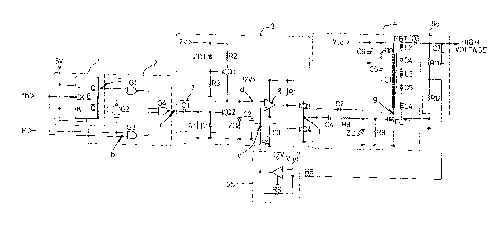
Referring to Fig. 2, an FBT driving apparatus for video
display appliances according to the present invention comprises a
horizontal frequency dividing section 1 for dividing the horizontal
frequency by a half in response to the input horizontal sync signal
fh, a horizontal frequency selecting section 2 for selecting and
outputting either the horizontal frequency or the divided
horizontal frequency provided from the horizontal frequency
dividing section 2 in response to the horizontal sync signal P, a
PWM modulating section 3 for modulating the horizontal frequency
selected by and supplied from the horizontal frequency selecting
section 2 and comparing the modulated horizontal frequency with the
error detection voltage to output the resultant circular wave pulse
signal, a high voltage generating section 4 for being driven by the
circular wave pulse signal to generate a high voltage, and error
detecting section 5 for detecting the high voltage supplied from
the high voltage generating section 4 and comparing the detected
21 83509
voltage with a reference voltage Vref to output the resultant
voltage as an error detection voltage.
The horizontal frequency dividing section 1 comprises a J-K-
type flip-flop 6 which divides the horizontal frequency of the
horizontal sync signal fh by a half in response to the horizontal
sync signal fh.
The horizontal frequency selecting section 2 comprises a
plurality of NAND gates Gl, G2, G3, G4 for selecting and outputting
either the horizontal frequency of the horizontal sync signal fh
or the divided horizontal frequency outputted from the J-K-type
flip flop 6 in response to a horizontal sync control signal P.
The PWM modulating section 3 includes a differentiation
circuit 7 for differentiating the signal supplied from the
horizontal frequency selecting section 2, a transistor Q2 switched
by the output of the differentiation circuit 7, and a comparator
8 for comparing the output signal from the transistor Q2 with the
error detection signal supplied from the error amplifier 5 to
output a resultant circular wave pulse signal.
The high voltage generating section 4 includes a field effect
transistor FETl, which is driven and controlled by the circular
wave pulse signal supplied from the PWM modulating section 3, and
a flyback transformer FBT for receiving the driving power supply
from the field effect transistor FETl at its primary winding to
induce a high voltage in its secondary winding.
The error detecting section 5 includes a high voltage
detecting circuit 5a comprising resistors R11, R12 for detecting
and feeding back the high voltage generated from the FBT, and an
error amplifier 5b for comparing the voltage detected by the
resistors R11, R12 with the reference voltage Vref to supply the
2 1 83509
- resultant voltage as an error detection voltage to the non-
inverting input terminal of the comparator 8.
Here, R1 to R10 refer to resistors; ZDl to ZD3 refer to Zener
diodes; Dl to D5 refer to diodes; Cl to C7 refer to capacitors; and
Q1, Q3, Q4 refer to transistors.
Operation of an FBT drivign apparatus for video display
appaliances can be described in detail with reference to Figs. 2,
3A to 3F and 4A to 4F.
Figs. 3A to 3F illustrate the waveforms at various points of
Fig. 2 when the horizontal sync control signal P goes 'high' due
to the input of low horizontal frequency. If a horizontal sync
signal fh of low frquency, for example, of below 60KHz as shown in
Fig. 3A is inputted, the horizontal sync control signal P goes
'high', and thus the NAND gate Gl of the horizontal frequency
lS selecting section 2 is turned off by the NAND gate G2, causing the
divided horizontal frequency outputted from the J-K-type flip-flop
6 as shown in Fig. 3B to be cut off by the NAND gate G2.
At this stage, the horizontal sync signal fh as shown in Fig.
3A which has not been divided by the NAND gates G3, G4 is supplied
to the differentiation circuit 7.
The horizontal sync signal fh inputted to the differentiation
circuit 7 is differentiated into the waveform as shown in Fig. 3D
('d' point in Fig. 2) and then supplied to the inverting input
terminal of the comparator 8 via transistor Q2. The comparator 8
compares the waveform at point 'd' supplied to its inverting input
terminal with the waveform at point 'e' in Fig. 3D which is
supplied from the error amplifier 5b to its non-inverting input
terminal to output a resultant circular wave pulse signal as
illustrated in Fig. 3E. The circular wave pulse signal drives the
21 8350q
~ field effect transistor FET1 of the high voltage generating section
4.
If the field effect transistor FET1 is driven by the circular
wave pulse signal, a driving power supply is provided to the
primary winding of the FBT, and thus a high voltage is induced in
the secondary winding of the FBT. The output high voltage from the
secondary winding of the FBT is then supplied to the following
circuits requiring the high voltage.
The output high voltage from the FBT is detected by the high
voltage detecting circuit 5a comprising resistors R11, R12, and
then supplied to the inverting input terminal of the error
amplifier 5b. The error amplifier 5b then compares the detected
voltage with the reference voltage Vref to supply the resultant
voltage to the comparator 8 as an error detection voltage.
As described above, the comparator 8 compares the error
detection voltage supplied from the error amplifier 5b with the
signal voltage provided from the differentiation circuit 7, and
supply the resultant circular wave pulse signal to the field effect
transistor FET1 to drive the field effect transistor FETl.
The driving power supply provided to the primary winding of
the FBT by the field effect transistor FET1 is evenly maintained
irrespective of the horizontal frequency changes to escalate the
high voltage driving efficiency of the FBT. The following is the
detailed description of the operation of the FBT.
As mentioned above, the comparator 8 compares the error
detection voltage with the signal voltage provided from the
differentiation circuit 7 as shown in Fig. 3D. In other words, the
comparator 8 senses the voltage difference between the two points
'e' and 'd' to change the duty of the resultant circular wave pulse
21 83509
signal according to the horizontal frequency as illustrated in Fig.
3E. The field effect transistor FET1 is thus driven by the
circular wave pulse signal of duty changes. Fig. 3F illustrates
the waveform appearing on the drain of the field effect transistor
FET1 according to the duty cycle of the horizontal pulse signal.
The driving power supply is provided to the primary winding of the
FBT by the output of the field effect transistor FET1. The high
voltage induced in the secondary winding of the FBT is amplified
by the coils L2, L4, and then multistage-rectified by the diodes
D3 to D5. The rectified voltage is smoothed by the capacitor C7,
and then supplied to the following circuits requiring the high
voltage.
Figs. 4A to 4F illustrate the waveforms at various points of
Fig. 2 when the horizontal sync control signal P goes 'low' by the
input horizontal frequency of higher than lOOKHz.
If the input horizontal sync control signal P is 'low', the
NAND gate G3 is turned off, while the NAND gate G1 is turned on.
The divided horizontal sync signal fh outputted from the J-K-type
flip-flop 6 as shown in Fig. 4B is supplied to the differentiation
circuit 7 through the NAND gate G4. The output voltage of the
differentiation circuit 7 is then applied to the comparator 8. The
FBT is driven by the aforementioned process and generates the high
voltage.
If the input horizontal frequency is 120KHz, the output of the
NAND gate G4 which receives the output of the J-K-type flip-flop
6 becomes 60KHz, since the flip-flop 6 divides 120Khz by a half.
In other words, the driving frequency of the FBT becomes half the
frequency of the input horizontal sync signal fh of high frequency.
As described above, an FBT driving apparatus according to the
2 1 83509
~ present invention employs a PWM-type circuit to maintain an even
power supply provided to the primary winding of the FBT as well as
to control the frequency for driving the FBT according to the input
horizontal frequency level. Accordingly, a horizontal frequency
of high frequency band does not result in deterioration of the FBT
efficiency or heat loss. The FBT driving apparatus according to
the present invention also enables construction of a circuit with
a low priced general FBT.