Note: Descriptions are shown in the official language in which they were submitted.
~18371 5
TECHNICAL FIELD
The present invention relates generally to fault location
in a paired line, and more particularly, to a device and method
for locating faults in a paired line by monitoring a current
induced in the paired line.
BACKGROUND OF THE INVENTION
A paired line is a conventional means of carrying
telecommunications transmissions. A paired line is typically
two balanced conductors individually insulated and twisted
together along their length in a spiral path. A plurality of
paired lines are usually bundled together to form a paired cable
containing up to one hundred or more paired lines, wherein each
paired line of the paired cable is capable of independently
carrying a telecommunications signal. A paired line is
generally an effective telecommunications carrier, however, a
fault can occasionally occur in a paired line limiting the
effectiveness thereof. For example, a resistance fault can
occur in a paired line when water invades the outer protective
covering of a paired cable through an imperfection or other flaw
therein. The resulting resistance fault is a resistive contact
between the two conductors of a paired line contained within the
paired cable. The resistance fault is also often accompanied by
a resistance from one of the two conductors of the paired line
to ground or to another conductor of the paired cable. Another
type of fault can occur when there is a discontinuity or break
in the shield of a paired cable. The fault allows an increased
coupling of extraneous voltages into one or more enclosed paired
lines from sources, such as power transmission cables, near the
paired cable.
Such faults typically cause noise in the affected paired
line that is extremely disruptive to the clarity of the
telecommunications signal sent over the paired line. A fault in
a paired line can also cause other problems such as circuit
failure, arc-over and corrosion. Therefore, it is desirable to
locate and repair faults in a paired line, particularly a paired
--1--
21837~5
line in a telecommunications cable.
Since telecommunications cables are not always readily
accessible, often being buried below ground, noninvasive methods
are preferred for locating faults in a paired line of a
telecommunications cable. Tone location methods are
conventional noninvasive means for locating a short fault in a
paired line of a telecommunications cable. In accordance with
one tone location method, an audible tone is placed across the
shorted conductors of the paired line by means of a tone
transmitter and the tone is followed to the fault by a pickup
coil placed on the paired line that is connected to an amplifier
and a headset worn by an operator. Because no tone current
flows past the short fault, the tone is audible up to the fault
and inaudible beyond the fault, allowing the operator to
precisely pinpoint the short fault to within a few centimeters
of its actual location.
This tone location method is ineffective, however, for
locating most resistance faults in a paired line. One reason
for such ineffectiveness is a phenomenon termed carry-by.
Carry-by occurs at faults that exceed a threshold resistance
typically above about 2000 ohms. Most resistance faults have a
resistance in a range between about 5000 to about 50,000 ohms.
When a resistance exceeding the threshold resistance for carry-
by is encountered at the resistance fault in a paired line, the
current of the audible tone produces a voltage across the
conductors of the paired line past the fault. This voltage
causes a corresponding tone current to flow into pair
capacitance beyond the fault. Thus, a tone will be audible
beyond the resistance fault defeating the present tone location
method. The problem of carry-by is particularly acute when a
high-frequency tone is present in the paired line, such as is
typically employed in the present tone location method, because
the magnitude of tone current flow past the fault is directly
related to the frequency of the tone.
It is further noted that the tone transmitter drives less
tone current through the paired line as the level of fault
--2--
2183715
resistance increases. At relatively high levels of resistance,
such as encountered in resistance faults, the level of tone
current available to the coil can drop below the background
noise level present on a paired cable. Consequently, the
background noise masks the location of the fault.
To overcome the limitations of the above-recited tone
location method caused by carry-by, another tone location method
has been developed in the telephone industry, wherein the
conductors of the paired line are welded together at the fault
using a 600-volt, breakdown test set. Welding of the conductors
reduces fault resistance to zero in the paired line, thereby
allowing effecti~e tone location of the resistance fault. This
tone location method, however, can cause extensive cable and
equipment damage, particularly to plastic insulated cable and
electronic central offices due to the high breakdown voltages
used. Accordingly, this tone location method for overcoming
fault resistance is disfavored.
An alternate tone location method for locating resistance
faults is disclosed in U.S. Patent 4,291,204, wherein a tone
locating device temporarily reduces the fault resistance to a
low value by establishing a transient arc at the fault. Passing
the fault locating tone through the low-resistance arc at the
fault reduces tone carry-by, but does not entirely eliminate it.
In addition, the conductors and equipment are susceptible to
damage caused by formation of the transient arc, albeit to a
lesser degree than the damage potential of the previous tone
location method.
Accordingly, it is an object of the present invention to
provide a device and method for effectively locating resistance
faults and other types of faults in a paired line using a
magnetic induced signal. It is a further object of the present
invention to provide a device and method for effectively
locating faults in a paired line using an induced signal,
wherein the device and method do not require formation of an arc
or a high-voltage weld at the fault. It is another object of
the present invention to provide a device and method for
--3--
2183715
effectively locating resistance faults and other types of faults
in a paired line using an induced signal, wherein the induced
signal is inaudible to listeners on adjacent paired lines of a
paired cable, yet detectable by the device, thereby minimizing
interference with normal operation of the paired cable. More
particularly, it is an object of the present invention to
provide a device and method for effectively locating faults in
a paired line using an induced signal, wherein the voltage and
frequency of the induced signal are such that background noise
is overcome while the impact of carry-by is minimized.
It is a further object of the present invention to provide
a device and method for effectively locating faults in a paired
line using an induced signal, wherein the device is fully
portable in the field for expeditiously tracking relatively long
lengths of the paired line. It is a still further object of the
present invention to provide a device and method for effectively
locating faults in a paired line using an induced signal that
assists the operator in distinguishing changes in the induced
signal due to depth variations from changes in the induced
signal due to the presence of a fault. It is yet another object
of the present invention to provide a device and method for
effectively locating breaks in a shield of a paired cable.
These objects and others are accomplished in accordance with the
invention described hereafter.
SUMMARY OF THE INVENTION
The present invention is a device and method for locating
a fault in a paired line. The device and method are
particularly applicable to the location of a resistance fault in
a paired line of a telecommunications cable. The fault locating
device comprises a base unit and a terminator unit each fixably
connectable to an opposite end of the two conductors of a
segment of a paired line believed to contain the fault. The
fault locating device further comprises a portable locator unit
movable along the conductors of the paired line segment between
the base unit and the terminator unit.
--4--
2183715
The locator unit has internal circuitry and an associated
coil that is positioned proximal to the conductors of the paired
line segment, such that the coil is in magnetic communication
but not electrical communication with the paired line. The
internal circuitry of the locator unit includes a small,
lightweight battery and a locator signal transmission circuit
for creating a locator signal in the coil which couples a
magnetic induced signal corresponding to the locator signal onto
the conductors of the paired line segment. The circuitry of the
locator unit also includes a carrier signal processing circuit
for receiving an encoded carrier signal traveling along the
conductors from the base unit, decoding the carrier signal and
communicating the decoded information to an operator in the form
of an indicator, such as an audible tone or a visual display.
The base unit has circuitry including an induced signal
receiver circuit for receiving the induced signal from the
locator unit via the conductors of the paired line segment and
a base carrier signal transmission circuit for creating and
sending a base carrier signal having synchronization markers and
values of a selected induced signal characteristic measured at
the base unit and terminator unit encoded thereon. The base
unit also has a terminator carrier signal receiver circuit for
receiving a terminator carrier signal having values of the
selected induced signal characteristic measured at the
terminator unit encoded thereon. The base unit further includes
noise nulling and synchronization circuitry for minimizing the
effect of noise and carry-over received over the induced signal
receiver circuit.
The terminator unit, like the base unit, has an induced
signal receiver circuit for receiving the induced signal from
the locator unit via the conductors of the paired line segment.
The terminator unit also has a terminator carrier signal
transmission circuit for creating and sending the terminator
carrier signal. In addition, the terminator unit has a base
carrier signal receiver circuit for receiving the base carrier
signal.
--5--
2183715
Operation of the fault locating device is performed by
positioning the locator unit along the paired line segment near
the base unit, wherein the fault is believed to be located
between the locator unit and the terminator unit. The locator
unit is activated, creating the magnetic induced signal on the
conductors of the paired line segment. The magnetic induced
signal travels along the conductors of the paired line segment
and is received by the base unit and terminator unit.
In response to receipt of the induced signal, the base unit
measures values of a selected induced signal characteristic at
the base unit and encodes these values along with
synchronization marks onto the base carrier signal. The base
unit sends the resulting encoded base carrier signal to the
locator unit. The terminator unit similarly measures values of
the selected induced signal characteristic at the terminator and
encodes these values onto the terminator carrier signal. The
terminator sends the encoded terminator carrier signal to the
base unit which additionally encodes the values from the
terminator carrier signal onto the base carrier signal. The
locator unit receives the base carrier signal, decodes the base
carrier signal and continuously communicates the decoded values
of the induced signal characteristic measured at the base unit
and terminator unit to the operator by means of an indicator.
The operator incrementally repositions the locator unit away
from the base unit and toward the terminator unit along the path
of the paired line segment as operation of the fault locating
device proceeds.
As the locator unit approaches the fault, the intensity or
frequency of the indicator remains substantially constant except
for some variation due to twisting of the conductors or changes
in the relative position of the coil and the paired line (e.g.,
depth changes). When the locator unit passes the fault,
however, so that the fault is between the locator unit and the
base unit, the intensity or frequency of the indicator abruptly
drops, thereby establishing the precise location of the fault.
It is noted that the voltage and frequency of the magnetic
--6--
21a371~
induced signal are narrowly specified in accordance with the
present invention to satisfy the performance requirements of the
fault locating device. In particular, the voltage and frequency
ranges of the induced signal are constrained at the upper end to
satisfy the requirements that the induced signal on the paired
line is inaudible to listeners and that the induced signal
avoids excessive carry-by. The voltage and frequency ranges of
the induced signal are constrained at the lower end to satisfy
the requirements that sufficient voltage is coupled onto the
paired line by the coil of the locator unit to provide an
induced signal exceeding background noise and that the resulting
induced signal is detectable by both the base and terminator
units.
Accordingly, the voltage and frequency of the induced
signal are balanced between an upper and lower limit to achieve
a fully-portable fault locating device having an inaudible, yet
detectable, magnetic induced signal, that exceeds the background
noise on the paired line while avoiding the effects of excessive
carry-by. Achievement of these performance requirements is
facilitated by noise nulling circuitry that reduces the noise on
the paired line and synchronization circuitry that mitigates the
impact of carry-by.
The present invention will be further understood, both as
to its structure and operation, from the accompanying drawings,
taken in conjunction with the accompanying description, in which
similar reference characters refer to similar parts.
BRIEF DESCRIPTION OF THE DRAWINGS
Figure 1 is a conceptual view of a fault locating device of
the present invention operably positioned in relation to a
paired line.
Figure 2 is a block diagram of the locator unit shown in
the device of Figure 1 configured to locate resistance faults in
a paired line.
Figure 3 is a block diagram of the base unit shown in the
device of Figure 1.
--7--
2183715
Figure 4 is a block diagram of the terminator unit shown in
the device of Figure 1.
Figures 5a, 5b, 5c depict conceptualized operation of a
synchronous detector employed in the base unit of Figure 3.
Figure 6 is a block diagram of the locator unit shown in
the device of Figure 1 configured to locate shield breaks in a
shielded cable.
DESCRIPTION OF PREFERRED EMBODIMENTS
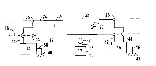
Referring initially to Figure 1, a fault locating device of
the present invention is shown and generally designated 10. The
fault locating device 10 has three basic components comprising
a locator unit 12, a base unit 14, and a terminator unit 16.
The fault locating device 10 is operably positioned relative to
a paired line 18, in which it is desired to locate a resistance
fàult 20, such that the base unit 14 engages a first conductor
22 and a second conductor 24 of the paired line 18 at a base
point 26 on the paired line 18 and the terminator unit 16
engages the first and second conductors 22, 24 at a terminator
point 28 on the paired line 18. The base point 26 and the
terminator point 28 are positioned at opposite ends of a segment
30 of the paired line 18 that is selected to encompass the fault
20, at least to the best approximation of the operator. If it
is subsequently determined that the selected paired line segment
does not encompass the fault, the paired line segment is simply
reselected until a paired line segment is selected encompassing
the fault in accordance with a method described hereafter. In
any case, for purposes of illustration, the paired line segment
30 of Figure 1 is shown to encompass the fault 20.
The fault locating device 10 of the present invention has
general utility to paired lines employed in a number of paired
cable applications, including power transmission and
communications paired cable applications. The fault locating
device 10 has particular utility to paired lines employed in
telecommunications paired cable applications, including
accessible paired cables, such as aerial paired cables, and
--8--
2183715
inaccessible paired cables, such as buried paired cables. As
defined herein, a paired line is substantially any line having
at least two continuous electrical conductors that, in the
absence of a fault, are electrically insulated from one another.
The two conductors can each be solid or braided wires, grounded
or ungrounded and having parallel or spiral paths.
Alternatively, one conductor can be a wire and the other
conductor can be a conductive tubular shield enclosing the wire.
The above-recited definition of a paired line encompasses
coaxial cable, shielded cable, and cable having more than two
conductors, wherein any two conductors of the cable may be
deemed to define a paired line for purposes of the invention.
For example, a paired line as defined herein includes a shielded
cable having a shield and a conductor enclosed within the
shield.
A fault is defined herein as any unintended perturbation in
the path of a conductor that undesirably draws current
therefrom, such as a short, a cross, a ground, or a split. For
purposes of illustration, the fault 20 disclosed herein is
characterized as a resistance fault, it being understood that
the device 10 is applicable to the location of many types of
faults as generally defined above.
The locator unit 12 is operably positioned proximal to a
locator point 32 on the paired line 18 that is between the base
point 26 and terminator point 28. As such, the locator unit 12
preferably does not electrically engage the conductors 22, 24,
but is sufficiently proximal to the conductors 22, 24 to produce
an induced signal therein as will be described hereafter. The
base and terminator points 26, 28 are preferably selected at
points on the paired line 18 where relatively convenient
electrical access to the conductors 22, 24 is provided, such as
a junction box or other splice location. Electrical
communication is provided between the base unit 14 and the
conductors 22, 24 by base pickup lines 34, 36 extending from the
base unit 14 and having electrically conductive pickups such as
conventional alligator clips or the like on the ends of the
g
2183715
lines 34, 36 that are removably connected to the conductors 22,
24. A base ground line 38 is also provided connecting the base
unit 14 to a ground 40. Similarly, electrical communication is
provided between the terminator unit 16 and the conductors 22,
24 by terminator pickup lines 42, 44 extending from the
terminator unit 16 and removably connected to the conductors 22,
24. A terminator ground line 46 is provided connecting the
terminator unit 16 to a ground 48.
As will be described in greater detail hereafter with
respect to the method of operation, the position of the base
point 26, and correspondingly the position of the base unit 14,
are substantially fixed with respect to the paired line 18
during a given fault locating sequence. The position of the
terminator point 28, and correspondingly the position of the
terminator unit 16, are likewise substantially fixed with
respect to the paired line 18 during a given fault locating
sequence. In contrast, the position of the locator point 32 is
variable along the length of the paired line 18 throughout a
given fault locating sequence as a function of the fixed
position of the fault 20 on the paired line 18. Accordingly,
the locator unit 12 has a fully mobile, unanchored, portable
configuration, the locator unit 12 being relatively compact and
lightweight to render it manually transportable by a single
operator. In the embodiment of Figure 1, the locator unit 12 is
shown to comprise a unitary housing 50 and a probe 52 positioned
outside the housing 50. A connective member 53 extends between
the probe 52 and the housing 50. The housing 50 is preferably
a hardened protective shell and the connective member 53 is
preferably a flexible or rigid tube. Although not shown, the
probe 52 can alternatively be positioned within the housing 50,
thereby eliminating the connective member 53.
The specific components of the locator unit 12 are
described with further reference to the block diagram of Figure
2. The probe 52 is shown schematically to enclose a coil 54
electrically connected by coil lines 56a, 56b to the circuitry
of the locator unit 12. The coil 54 can have a number of
-10-
- ` 2183715
configurations depending on the specific application of the
fault locating device 10. For locating faults in an
inaccessible paired line, a relatively large remote coil is
provided, typically having an elongated magnetic core or other
geometry sufficient to meet the performance requirements of the
locator unit 12. For locating faults in an accessible paired
line, a relatively small contact coil is provided.
The circuitry of the locator unit 12 comprises a locator
signal transmission circuit 58 and a carrier signal processing
circuit 60. The locator signal transmission circuit 58 provides
a pathway from a microcontroller 62 to the coil 54 for a locator
signal capable of producing a magnetic induced signal in the
paired line 18. Included in series within the locator signal
transmission circuit 58 in a direction away from the
microcontroller 62 toward the coil line 56a are a synchronized
oscillator 64, a locator signal power driver 66, and a carrier
signal rejection filter 68. The locator signal transmission
circuit 58 and the carrier signal processing circuit 60 are in
electrical communication with the coil 54 via the coil line 56a.
The carrier signal processing circuit 60 provides a pathway
for a carrier signal from the coil 54 to the microcontroller 62.
Included in series within the carrier signal processing circuit
60 in the direction away from the coil line 56a toward the
microcontroller 62 are a locator signal rejection filter 72, a
carrier signal preamplifier 74, a switch 76 and a carrier signal
receiver 78. The carrier signal processing circuit 60 splits
into two parallel pathways after the carrier signal receiver 78
with a first parallel pathway 80 including a limiter 82 and a
decoder 84 and a second parallel pathway 86 including a
magnitude detector 88. As used herein, the term "limiter" is
defined to encompass a conventional limiter or, in the
alternative, an automatic gain control.
The first and second parallel pathways 80, 86 feed into the
microcontroller 62 through an analog to digital converter 90.
The locator unit 12 is further provided with a visual display 92
and an audio speaker 94 in parallel electrical communication
21 8371 5
with the microcontroller 62, enabling the locator unit 12 to
communicate an indicator both visually and audibly to an
operator of the device 10.
The microcontroller 62 disclosed herein is a digital
microprocessor. It is nevertheless apparent to the skilled
artisan that within the scope of the present invention an analog
controller can be substituted for the digital microprocessor
within the circuits 58, 60 without substantially altering the
capabilities of the present fault locating device 10. The
analog to digital converter 90 is omitted from the carrier
signal processing circuit 60 in the case where an analog
controller is substituted for a digital microprocessor as the
microcontroller 62. A DC power source 96 is additionally
included in the housing 50 of the locator unit 12. The power
source 96 supplies power to the components of the locator unit
12 enabling the functions thereof. The power source 96 is
preferably a relatively small, lightweight battery pack, such as
one or more dry-cell or rechargeable batteries (e.g., 9-volt or
D-cell batteries).
It is noted that the microcontroller 62, synchronized
oscillator 64 and decoder 84 are shown and described herein as
discrete structural components having related functions. In
practice, these discrete components can be integrated into a
single digital microprocessor structure performing the same
functions ascribed to the discrete components in a manner
apparent to the skilled artisan.
It is additionally noted that the switch 76 of locator unit
12 has two functional positions providing alternate capabilities
therefor. When the switch 76 is in the position shown, the coil
54 and carrier signal processing circuit 60 function as a
magnetic carrier signal pickup, primarily for receiving magnetic
carrier signals from the base unit 14 as described hereafter.
By selectively repositioning the switch 76, a capacitive ground
reference circuit 98 is enabled which, in cooperation with the
coil 54, functions as a capacitive pickup primarily for locating
cable shield breaks as described hereafter. The capacitive
- 12 -
2183715
ground reference circuit 98 includes a capacitive ground
reference 100 and a capacitive signal preamplifier 102 on one
side of the switch 76. The remainder of the capacitive ground
reference circuit 98 on the opposite side of the switch 76 is
identical to the carrier signal processing circuit 60, including
the carrier signal receiver 78, first and second parallel
pathways 80, 86, analog to digital converter 90 and
microprocessor 62.
If the housing 50 of the locator unit 12 is electrically
conductive, the capacitive ground reference 100 is simply the
housing 50. If the housing 50 is not electrically conductive,
however, the capacitive ground reference 100 can be provided by
a metallic shield (not shown) contained within the housing 50.
In either case, the capacitive ground reference 100 couples to
the body of an operator, which provides adequate ground
reference for a carrier signal when the operator is standing on
the earth. Although not shown, the capacitive ground reference
100 can alternatively be a grounding lead and grounding
connection connected to a cable shield.
It is further noted that the circuitry of the locator unit
12 further comprises a locator circuit common 104. The locator
circuit common 104 is electrically connected to the locator
signal power driver 66, carrier signal preamplifier 74 and
capacitive carrier preamplifier 102.
The specific components of the base unit 14 are described
with further reference to the block diagram of Figure 3.
Substantially all of the circuitry of the base unit 14 is
enclosed in a housing 200 comprising a hardened protective
shell. The circuitry of the base unit 14 includes an induced
signal receiver circuit 202 and a base unit carrier signal
transmission circuit 204. As described above, the base pickup
lines 34, 36 extend from the base unit 14 and removably connect
with the conductors 22, 24 to provide electrical communication
between the circuits 202, 204 and the paired line 18. The
induced signal receiver circuit 202 is configured to receive the
induced signal originating at the locator point 32 and sent
-13 -
21837~5
therefrom along the paired line 18. Included in series within
the induced signal receiver circuit 202 in a direction away from
the paired line 18 are a variable gain amplifier 206, a bandpass
filter 208, a synchronous detector 210, a lowpass filter 212, an
analog to digital converter 214 and a microcontroller 216.
Incorporated within the induced signal receiver circuit 202 is
a low impedance input termination 218 positioned between the
base pickup lines 34, 36 and the variable gain amplifier 206.
The low impedance input termination 218 comprises a first
inlet pathway 220 and a second inlet pathway 222. The first
inlet pathway 220 is connected to a base circuit common 224
through a first balanced resistor 226 and a first balanced
capacitor 228 in parallel. The second inlet pathway 222 is
connected to the base circuit common 224 through a second
balanced resistor 230 and a second balanced capacitor 232 in
parallel. The first and second balanced resistors 226, 230 are
substantially equal in resistance to provide, in series, an
input terminating resistance across the base pickup lines 34,
36. As such, the first and second balanced resistors 226, 230
provide a balanced center tap of the low impedance input
termination 218 connected to the base circuit common 224. The
first and second balanced capacitors 228, 232 are also
substantially equal in value to provide a relatively low
impedance path from the base pickup lines 34, 36 to the base
circuit common 224 for the higher frequency carrier signals
while providing a balanced relatively high impedance to the
lower frequency induced signal. The first and second inlet
pathways 220, 222 feed into a differential signal preamplifier
234 that is connected in series to a summing amplifier 236 and
the variable gain amplifier 206.
A line balancing pathway 238 is provided having a balancing
switch 240 that enables selective connection of the first or
second inlet pathway 220 or 222 to the base grounding line 38
through a line balancing variable impedance 242. The base
ground line 38 is connected to the ground 40 by a ground pickup
244. A switching line 246 extends from the base ground line 38
-14-
2183715
having a resistor 248 and a grounding switch 250 in series.
When closed, the grounding switch 250 connects the base circuit
common 224 to the ground 40 through the resistor 248.
A noise nulling circuit 252 feeds into the low impedance
5 input termination 218 from the base ground line 38. The noise
nulling circuit 252 includes in series a variable gain amplifier
254, a variable phase shifter 256, and a three-way switch 258.
A first position of the switch 258 connects the noise nulling
circuit 252 with the first inlet pathway 220 through a first
summing impedance 260, a second position of the switch 258
connects the noise nulling circuit 252 with the second inlet
pathway 222 through a second summing impedance 262, and a third
position of the switch 258 connects the noise nulling circuit
252 with the summing amplifier 236 through a summing input line
263.
The base carrier signal transmission circuit 204 is
configured to send an encoded carrier signal from the base unit
14 along the paired line 18 to the locator unit 12 and the
terminator unit 16. Included in series within the base carrier
20 signal transmission circuit 204 in the direction of the paired
line 18 are the microcontroller 216, an encoder 264, and a
carrier signal driver 266. A carrier signal oscillator 268
electrically communicates with the encoder 264 and a locator
synchronization osciIlator 269 is provided in electrical
25 communication with the microcontroller 216 and the synchronous
detector 210. The carrier signal driver 266 is referenced to
the base circuit common 224 and connected to the base grounding
line 38 through a capacitor 270.
The base unit 14 is also provided with a terminator carrier
30 signal receiver circuit 272 configured to receive an encoded
carrier signal originating at the terminator unit 16 and sent to
the base unit 14 along the paired line 18. The carrier signal
receiver circuit 272 is connected to the base ground line 38
through a capacitor 274. Included in series within the
35 terminator carrier signal receiver circuit 272 in a direction
away from the capacitor 274 are a carrier signal receiver 276,
-15 -
2183715
a limiter 278, a decoder 280, and the microcontroller 216. The
microcontroller 216 disclosed herein is a digital
microprocessor. It is nevertheless apparent to the skilled
artisan that within the scope of the present invention an analog
controller can be substituted for the digital microprocessor
within the circuits 202, 204, 272 without substantially altering
the capabilities of the present fault locating device 10. The
analog to digital converter 214 is omitted from the induced
signal receiver circuit 202 in the case where an analog
controller is substituted for a digital microprocessor as the
microcontroller 216. A DC power source 282 is additionally
included in the housing 200 of the base unit 14. The power
source 282 supplies power to the components of the base unit 14
enabling the functions thereof. The power source 282 is
preferably one or more relatively small, lightweight batteries.
It is noted that the microcontroller 216, encoder 264,
decoder 280 and oscillators 268, 269 are shown and described
herein as discrete structural components having related
functions. In practice, these discrete components can be
integrated into a single digital microprocessor structure
performing the same functions ascribed to the discrete
components in a manner apparent to the skilled artisan.
The specific components of the terminator unit 16 are
described with further reference to the block diagram of Figure
4. Substantially all of the circuitry of the terminator unit 16
is enclosed in a housing 400 comprising a hardened protective
shell. The circuitry of the terminator unit 16 includes an
induced signal receiver circuit 402 and a terminator carrier
signal transmission circuit 404. As described above, the
terminator pickup lines 42, 44 extend from the terminator unit
16 and connect with the conductors 22, 24 to provide electrical
communication between the circuits 402, 404 and the paired line
18. The induced signal receiver circuit 402 is configured to
receive the induced signal originating at the locator point 32
and sent therefrom along the paired line 18. Accordingly, the
induced signal receiver circuit 402 of the terminator unit 16 is
-16-
2183715
substantially similar to the induced signal receiver circuit 202
of the base unit 14 shown in Figure 3. Included within the
induced signal receiver circuit 402 in a direction away from the
paired line 18 are a variable gain amplifier 406, a bandpass
filter 408, a synchronous detector 410, a lowpass filter 412, an
analog to digital converter 414 and a microcontroller 416.
Further included within the induced signal receiver circuit 402
is a high impedance input termination 418 positioned between the
terminator pickup lines 42, 44 and the variable gain amplifier
406. The high impedance input termination 418 is specified to
provide a relatively high impedance to the induced signal
voltage so that the terminator unit 16 does not draw induced
signal current past the fault as is described hereafter.
The high impedance input termination 418 comprises a first
inlet pathway 420 and a second inlet pathway 422. The first
inlet pathway 420 is connected to a terminator circuit common
424 through a first balanced resistor 426 and a first balanced
capacitor 428 in parallel. The second inlet pathway 422 is
connected to the terminator circuit common 424 through a second
balanced resistor 430 and a second balanced capacitor 432 in
parallel. The first and second balanced resistors 426, 430 are
substantially equal in resistance, having a relatively high
value on the order of about 1 megohm to provide in series an
input terminating resistance across the terminator pickup lines
42, 44. As such, the first and second balanced resistors 426,
430 provide a balanced center tap of the high impedance input
termination 418 connected to the terminator circuit common 424.
The first and second balanced capacitors 428, 432 are also
substantially equal in value to provide a relatively low
impedance path from the terminator pickup lines 42, 44 to the
terminator circuit common 424 for the higher frequency carrier
signals while providing a balanced relatively high impedance to
the lower frequency induced signal. The first and second inlet
pathways 420, 422 feed into a differential signal preamplifier
434 that is connected in series to the variable gain amplifier
406.
-17-
2 1 83 7 ! 5
The terminator carrier signal transmission circuit 404 is
configured to send an encoded carrier signal from the terminator
unit 16 along the paired line 18 to the base unit 14.
Accordingly, the carrier signal transmission circuit 404 of the
5 terminator unit 16 is substantially similar to the carrier
signal transmission circuit 204 of the base unit 14 shown in
Figure 3. Included in series within the terminator carrier
signal transmission circuit 404 in the direction of the paired
line 18 are the microcontroller 416, an encoder 436, and a
carrier signal driver 438. A carrier signal oscillator 440
communicates with the encoder 436. The carrier signal driver
438 is connected to the terminator ground line 46 through a
capacitor 442 and a terminator ground pickup 444. A terminator
synchronization oscillator 446 is provided in electrical
communication with the microcontroller 416 and the synchronous
detector 410.
The terminator unit 16 is also provided with a base carrier
signal receiver circuit 448 configured to receive an encoded
carrier signal originating at the base unit 14 and sent to the
terminator unit 16 along the paired line 18. The carrier signal
receiver circuit 448 is connected to the terminator ground line
46 through a capacitor 450. Included in series within the base
carrier signal receiver circuit 448 in a direction away from the
capacitor 450 are a carrier signal receiver 452, a limiter 454,
a decoder 456, and the microcontroller 216.
The microcontroller 416 disclosed herein is a digital
microprocessor. It is nevertheless apparent to the skilled
artisan that within the scope of the present invention an analog
controller can be substituted for the digital microprocessor
within the circuits 402, 404 without substantially altering the
capabilities of the present fault locating device 10. The
analog to digital converter 414 is omitted from the induced
signal receiver circuit 402 in the case where an analog
controller is substituted for a digital microprocessor as the
microcontroller 416. A DC power source 458 is additionally
included in the housing 400 of the terminator unit 16. The
-18-
2183715
power source 458 supplies power to the components of the
terminator unit 16 enabling the functions thereof. The power
source 458 is preferably one or more relatively small,
lightweight batteries.
It is noted that the microcontroller 416, encoder 436,
decoder 456 and oscillators 440,-446 are shown and described
herein as discrete structural components having related
functions. In practice, these discrete components can be
integrated into a single digital microprocessor structure
performing the same functions ascribed to the discrete
components in a manner apparent to the skilled artisan.
Method of O~eration
Operation of the fault locating device 10 is described with
reference to Figures 1-4. At the outset, a segment 30 of a
paired line 18 is identified that is believed to contain a fault
20. The paired line segment 30 is typically up to about 5000
meters in length and can comprise the entire length of the
paired line 18, if the paired line is 5000 meters or less in
length. The base unit 14 is fixably positioned at a base point
26 that is at one end of the paired line segment 30 and the
terminator unit 16 is fixably positioned at a terminator point
28 that is at the other end of the paired line segment 30. The
base pickup lines 34, 36 are removably connected to the first
and second conductors 22, 24 at the base point 26 and the
terminator pickup lines 42, 44 are similarly removably connected
to the first and second conductors 22, 24 at the terminator
point 28.
The method of locating the fault 20 is initiated by
positioning the probe 52 of the locator unit 12 proximal to a
selected locator point 32 on the paired line 18 between the base
point 26 and terminator point 28. The actual position of the
locator point 32 is variable, rather than fixed, during
operation of the fault locating device 10. The locator point 32
is preferably positioned near the base point 28 during initial
operation of the device 10 such that the fault 20 is located
-19-
2183715
somewhere along the paired line segment 30 between the locator
point 32 and the terminator point 28. The locator point 32 is
then incrementally repositioned toward the terminator point 28
as operation of the device 10 proceeds. The relative distance
between the probe 52 and conductors 22, 24 at any given locator
point 32 is termed the induction distance. The maximum
allowable induction distance is a function of the power output
of the locator unit 12, the size and configuration of the coil
54, and the desired voltage of the signal induced in the
conductors 22, 24. A typical maximum allowable induction
distance is up to about 1 meter using a relatively large remote
induction coil 54 for inaccessible buried paired cable and up to
about 0.06 meters using a relatively smaller contact induction
coil 54 for accessible paired cable.
The microprocessor 62 directs the synchronized oscillator
64 and locator signal power driver 66 to generate a synchronized
AC locator signal utilizing the DC power source 96. The
resulting locator signal is sent to the coil 54 via the locator
signal transmission circuit 58 where the coil 54 magnetically
couples the locator signal into the paired line 18 to produce a
magnetic induced signal in the paired line 18 at the locator
point 32. The voltage and frequency of the induced signal are
selected within ranges that satisfy the performance requirements
of the fault locating device 10. In particular, the voltage and
frequency ranges of the induced signal are limited at the upper
end by the requirement that the induced signal on the paired
line 18 be inaudible to listeners and by the requirement that
the induced signal on the paired line 18 avoid excessive carry-
by. Generally, a signal having both a very low voltage and a
very low frequency satisfies the requirements of being inaudible
and avoiding significant carry-by. Such a signal, however, may
fail to satisfy other performance ~equirements of the device 10,
lacking sufficient voltage to exceed the background noise and
lacking sufficient frequency to be coupled onto the paired line
18 by the coil 54. If the frequency of the induced signal is
raised to improve the detectability thereof, the induced signal
-20-
21~3715
may become overly susceptible to carry-by. Alternatively, if
the voltage of the induced signal is raised to overcome the
background noise, excessive battery power may become necessary,
defeating the portability of the detector unit 12. Particularly
high background noise levels are observed where resistance
between the conductors 22, 24 creates an unbalanced condition in
the paired line 18 that allows the induced 50/60 Hz voltage and
35 Hz noise normally present common mode to ground on the
conductors 22, 24 of the paired line 18 to be coupled into the
paired line 18, appearing as differential noise between the
conductors 22, 24.
The present invention recognizes that selection of the
voltage and frequency of the induced signal requires a balancing
of competing factors to achieve the required fully-portable
fault locating device 10 having an inaudible, yet detectable,
induced signal, that exceeds the background noise on the paired
line 18 while avoiding the effects of excessive carry-by.
Achievement of these performance requirements is facilitated by
noise nulling circuitry that reduces the noise on the paired
line 18 and synchronization circuitry that mitigates the impact
of carry-by, as described hereafter. As such, the frequency of
the induced signal is typically selected in a range less than
about 300 Hz, preferably in a range between about 200 Hz and
about 1 Hz, and most preferably at a value of about 35 Hz. The
corresponding voltage of the induced signal is typically
selected in a range between about 0.1 microvolt and 100
microvolts and preferably at a value of about 1 microvolt, which
is generally greater than ambient noise after noise nulling.
The induced signal satisfying the above-recited criteria
travels along the conductors 22, 24 to the base unit 14 and the
terminator unit 16. With the locator point 32 positioned
between the base point 26 and the fault 20, the base pickup
lines 34, 36 receive the induced signal and carry the induced
signal to the induced signal receiver circuit 202 having the
noise nulling circuitry incorporated therein. The differential
signal preamplifier 234 amplifies the induced signal received by
-21-
2183715
the low impedance input termination 218 from the base pickup
lines 34, 36. The differential signal preamplifier 234 is also
equipped with a DC blocking mechanism to remove DC biases
present on the paired line 18. The summing amplifier 236 adds
the output of the differential signal preamplifier 234 to the
output of the noise nulling circuit 252 enabling the operator to
reduce the effects of noise on the conductors 22, 24 received by
the base unit 14. In particular, noise nulling enables the
operator to cancel the unbalanced voltage on the paired line 18
by summing a portion of the common mode voltage present between
the conductors 22, 24 and the ground 40 at the base point 26
with the differential voltage present across the paired line 18,
in proper phase and magnitude. Summing of these voltages causes
substantial cancellation of the noise induced onto the paired
line 18 by the unbalance often present at the fault 20.
The noise nulling circuitry effectuates noise nulling by
means of the low impedance input termination 218. The first and
second balanced resistors 226, 230 of the low impedance input
termination 218 are connected to the base circuit common 224
having a high impedance to earth ground, thereby functioning to
reject common mode signals to ground while referencing the base
circuit common 224 to the common mode (longitudinal) voltage
present on the conductors 22, 24. The low impedance input
termination 218 is augmented by selecting one or more of the
noise nulling techniques described hereafter that are enabled by
the circuitry of the base unit 14.
In accordance with a technique termed summing amplifier
nulling, the common mode voltage of the induced signal between
the conductors 22, 24 and the ground 40 is processed by the
variable gain amplifier 254 and the variable phase shifter 256
and summed into the summing amplifier 236. The gain and phase
of the induced signal are adjusted to null the imbalance voltage
beyond the summing amplifier 236. An alternate technique termed
summing impedance nulling likewise processes the common mode
voltage with the variable gain amplifier 254 and the variable
phase shifter 256. The resulting signal, however, is applied to
-22 -
2183715
one side of the low impedance input termination 218 through the
summing impedance 260, 262 or a resistor (not shown) substituted
therefor, while the switch 258 disconnects the summing input
line 263 causing the summing amplifier 236 to function as a
5 buffer amplifier for signals from the differential signal
preamplifier 234. Proper adjustment of the gain and phase
balances out the noise at the input to the differential signal
preamplifier 234 and simultaneously reduces the noise level on
the conductors 22, 24.
In accordance with a technique termed line balancing
variable impedance adjustment, the common mode voltage on either
the first or the second inlet pathway 220, 222, as selected by
the switch 230, is passed through the line balancing variable
impedance 242, selecting whichever inlet pathway 220 or 222
produces the greatest noise cancellation. If required, the line
balancing variable impedance 242 is also adjusted to minimize
noise. This technique is particularly effective when the
unbalance is very large, such as in the case of unbalanced
shunting impedances, and may be supplemented by either of the
two previously recited techniques.
A technique termed line balancing with grounded termination
center tap also has utility in conjunction with either of the
previously recited techniques. In accordance with this
technique, the grounding switch 250 is closed, effectively
grounding the center tap of the low impedance input termination
218. The switch 240 is closed to the side of the inlet pathway
220 or 222 producing the greatest noise cancellation. The line
balancing variable impedance 242 is then adjusted, if required,
to mlnlmlze nolse.
The output of the summing amplifier 236 passes to the
variable gain amplifier 206 where the voltage of the induced
signal is further amplified and, if desired, adjusted for
differences in the signal due to fault resistance losses. The
bandpass filter 208, which is tuned to the relatively low
frequency of the induced signal, rejects extraneous signals from
the output of the variable gain amplifier 206 that have
-23 -
21 8371 5
surrounding frequencies. In particular, the bandpass filter 208
attenuates interference from 50/60 Hz signals that are
magnetically induced onto the paired line 18 by adjacent power
llnes .
The synchronous detector 210 is driven by the locator
synchronization oscillator 269 which is synchronized with
generation of the locator signal at the locator unit 12, thereby
synchronizing operation of the base unit 14 and locator unit 12.
Synchronous operation of the base unit 14 and locator unit 12 in
conjunction with the use of an induced signal having a
relatively low frequency enables the effective location of
faults having resistances above 50 kohms without a significant
impact from carry-by, even in relatively long paired line
segments 30 having lengths up to 5000 meters. Low frequency
operation tends to decrease carry-by because lowering the
frequency of the induced signal increases the capacitive
reactance of the paired line 18, reducing the magnitude of
induced signal current flow past the fault 20. The synchronous
detector 210 supplements this effect by detecting only the
current of the induced signal flowing through the fault
resistance and rejecting any carry-by occurring due to current
flow into capacitance that leads resistive current by 90. The
low frequency induced signal has the added advantage of
exhibiting substantially less attenuation over length of the
paired line segment 30 than would a higher frequency induced
signal. Synchronous detection further enables the operator to
observe changes in polarity due to twisting of the conductors
22, 24. This permits the operator to differentiate between
carry-by and the induced signal in the presence of unbalanced
conductor faults and ground faults both of which are more
susceptible to carry-by than balanced conductor faults.
The principle by which the synchronous detector 210
operates is described with reference to Figure 5a, 5b and 5c.
Operation of the synchronous detector 210 in association with
the fault locating device 10 of Figure 1 is the functional
equivalent of a circuit 600 shown in Figure 5a. The circuit 600
-24-
2183715
has a switch 602 that is opened and closed in synchronism with
the induced signal at the locator unit 14. The circuit 600
further includes a series resistor 604 and, in parallel, a
resistor 606, a capacitor 608 and an amplifier 610 such that the
output voltage of the circuit 600 is the average input voltage
of the circuit 600 when the switch 602 is closed. The switch
602 is opened and closed as shown in Figure 5b by the switch
waveform 612. Figure 5c shows the input voltage waveform of the
circuit 600 as the sum of two distinct waveforms, a resistance
current waveform 614 and a capacitance current waveform 616.
By opening and closing the switch 602 in synchronism with
the input voltage waveform, in accordance with the relationship
shown in Figures 5b and 5c, the capacitance current waveform 616
of the carry-by leads the resistance current waveform 614 by
90, thereby averaging to zero as indicated by the shaded area
under the capacitance current waveform 616 of Figure 5c. In
contrast, the entire fault resistance current waveform 614 is in
phase with the induced signal and the switch waveform 612,
thereby enabling detection of the resistance fault.
Referring again to Figure 3 and the operation of the base
unit 14, the lowpass filter 212 filters the rectified DC signal
from the synchronous detector 210, allowing a narrowing of the
circuit bandwidth to more effectively filter out 50/60Hz signals
and other extraneous signals having undesired frequencies. The
analog to digital converter 214 converts the analog voltage
values of the DC signal produced by the lowpass filter 212 to
digital values for processing by the microcontroller 216 which
is shown herein to be a digital microprocessor. It also is
within the purview of the skilled artisan to substitute an
analog controller for a digital microprocessor as the
microcontroller 216, in which case the analog to digital
converter 214 is omitted from the base unit 14. In either case,
the microcontroller 216 configures the circuitry of the base
unit 14 for its various modes of operation, including receiving
and reading the induced signal and encoding and sending a
carrier signal. In particular, the microcontroller 216
-25-
2 1 83 7 ! 5
specifies values of an induced signal characteristic that are
encoded onto a carrier signal created by the base unit 14 and
sent to the locator unit 12. For purposes of fault location,
the induced signal is disclosed herein as being characterized in
5 terms of the magnitude of its voltage. However, it is
understood that within the scope of the present invention, the
induced signal can alternatively be specified in terms of
characteristics other than voltage magnitude, such as phase
shifts.
Regardless of which characteristic is selected to specify
the induced signal, the carrier signal transmission circuit 204
of the base unit 14 creates a carrier signal having values of
the selected characteristic for the induced signal and having
synchronization marks encoded therein. The synchronization
marks enable the locator unit 12 to create the induced signal in
synchronization with operation of the synchronous detector 210
at the base unit 14 so that carry-by is reduced. For example,
the encoded base carrier signal is created by delivering values
of the voltage magnitude of the induced signal measured at the
base unit 12 from the microcontroller 216 to the encoder 264.
The synchronization marks are similarly delivered from the
microcontroller 216 to the encoder 264. The encoder 264
imprints this information onto the base carrier signal in the
form of a digital or analog code.
The encoded base carrier signal is sent in synchronization
with the locator unit 12 by means of the carrier signal
oscillator 268 and carrier signal driver 266 to the locator unit
12. In particular, the carrier signal driver 266 drives the
carrier signal current out through the capacitor 270 and ground
pickup 244 to the ground 40, forcing an opposing current flow
from the carrier signal driver 266, into the base circuit common
224, through the first and second balanced capacitors 228, 232,
into the base pickup lines 34, 36, and onto the paired line 18.
The capacitor 270 provides a low impedance path to the ground 40
for the carrier signal while providing a high impedance for the
induced signal from the locator unit 12. Unlike the induced
- 26 -
218371~
signal, the encoded base carrier signal has a frequency range
greater than about 5 kHz, preferably a frequency range between
about 5 kHz and about 100 kHz, and most preferably a frequency
value of about 10 kHz. The encoded base carrier signal
typically has a voltage below about 150 volts within the
prescribed frequency range and preferably has a voltage of about
25 volts.
When the encoded base carrier signal reaches the locator
unit 12 via the conductors 22, 24, the base carrier signal is
received magnetically by the coil 54 within the probe 52
positioned at the locator point 32. The base carrier signal is
sent along the coil line 56a to the carrier signal receiver
circuit 60 while entry to the locator signal transmission
circuit 58 is blocked by means of the carrier signal rejection
filter 68. The carrier signal passes through the locator signal
rejection filter 72, which blocks entry of the locator signal
into the carrier signal processing circuit 60, and is fed to the
carrier signal preamplifier 74. The carrier signal is amplified
in the carrier signal preamplifier 74 and delivered to the
carrier signal receiver 78 through the closed switch 76. The
carrier signal receiver 78 feeds the amplified signal to the
limiter 82 where the amplitude of the signal is limited thereby
and then to the decoder 84 where the encoded information on the
carrier signal is read. The decoded information, which
comprises the synchronization marks and values of the selected
characteristic specifying the induced signal (in this case
voltage magnitude measured at the base unit 14), is transmitted
from the decoder 84 to the microcontroller 62 for processing
after the decoded information is passed through the analog to
digital converter 90 for digital conversion.
The magnitude detector 88 simultaneously evaluates the
amplified signal from the carrier signal receiver 78 to
determine the magnitude of the carrier signal for processing by
the microcontroller 62, whether the signal has originated from
the magnetic carrier receiver circuit 58 or the capacitive
ground reference circuit 102, as will be described hereafter.
-27-
2183715
The magnitude detector 88 sends values of the magnitude of the
carrier signal to the microcontroller 62 after it has passed
through the analog to digital converter 90 for digital
conversion. As previously noted, it is within the purview of
5 the skilled artisan to substitute an analog controller for a
digital microprocessor as the microcontroller 62, in which case
the analog to digital converter 90 is omitted from the locator
unit 12.
The microcontroller 62 directs operation of the
synchronized oscillator 64, display 92, speaker 94 in
correspondence with the decoded information received from the
decoder 84. For example, the synchronization marks are
translated into instructions that are sent to the synchronized
oscillator 64 for synchronized operation thereof. Values of the
voltage magnitude for the induced signal are similarly
translated into instructions that are sent to the speaker 94 for
generating a audible correlation of the voltage magnitude in the
form of a continuous audible tone having an intensity or
frequency directly related to the values of the voltage
magnitude for the induced signal received by the base unit 14.
As the voltage magnitude increases, the intensity or frequency
of the tone generated by the speaker 94 increases.
Correspondingly, as the voltage magnitude decreases, the
intensity or frequency of the tone generated by the speaker 94
decreases.
The presence of the fault 20 causes a drop in the magnitude
of the voltage for the induced signal, because the voltage of
the induced signal divides between the resistance of the fault
20 and the low resistance of the low impedance input termination
218 of the base unit 14. When the fault resistance draws
current, current also flows through the low impedance input
termination 218 producing a voltage drop detectable by the base
unit 14. If the locator unit approaches the fault 20 from the
base point 26, the base unit 14 will detect voltage due to
current flow in the fault resistance. The magnitude of this
voltage may rise and fall and reverse in polarity as the coil 54
-28 -
21~3715
is moved along the paired cable containing the paired line
segment 30 due to the twist of the conductors 22, 24 and the
spiraling of the paired line segment 30 within the paired cable,
but will remain continuous before the fault 20 is reached.
5 Polarity changes can be communicated to the operator by a change
in a characteristic of the audible tone in correspondence with
polarity changes. In any case, when the locator unit 12 passes
the fault 20, the base unit 14 no longer detects any voltage,
while the terminator unit 16 detects full voltage as described
hereafter.
Thus, the fault 20 in the segment 30 of the paired line 18
is located by shifting the locator unit 12 along the segment 30
away from the base point 26 in the direction of the terminator
point 28 to establish incrementally new locator points 32
15 therebetween. The fault 20 is precisely located at the point on
the segment 30 where the intensity or frequency of the tone from
the speaker 94 is strong followed by an abrupt drop in the
intensity or frequency of the tone as the locator unit 12
continues in the direction of the terminator point 28. The
20 display 92 provides a quantitative visual verification of the
information communicated to the operator by the speaker 94. The
display 92 is a visual correlation of the voltage magnitude in
the form of either an analog or a digital readout of the values
of the voltage magnitude for the induced signal as the locator
25 unit 12 is conveyed along the paired line 18.
The terminator unit 16 supplements the present method of
fault location by providing an auxiliary encoded carrier signal
responsive to the induced signal of the locator unit 12. The
encoded carrier signal of the terminator unit 16 confirms
30 location of the fault 20 when read in conjunction with the
encoded carrier signal of the base unit 14. In operation, the
induced signal originating at the locator point 32 travels to
the terminator point 28 where it is received by the terminator
unit 16 and processed in a manner similar to that of the base
35 unit 14. In particular, the induced signal is delivered from
the conductors 22, 24 to a high impedance input termination 418
-29-
~1837~5
by the terminator pickup lines 42, 44 that are removably
connected to the conductors 22, 24. The high impedance input
termination 418 is balanced in substantially the same manner as
the low impedance input termination 218 of the base unit 14, but
lacks the associated noise nulling circuitry of the base unit 14
because the termination unit 16 receives a stronger signal than
the base unit 14 that is not attenuated by fault resistance.
The termination unit 16 also has a high input impedance
preventing it from drawing the induced signal when the locator
unit 12 is between the fault 20 and the terminator unit 16.
The differential signal preamplifier 434 receives the
induced signal from the high impedance input termination 418 and
amplifies the induced signal. The output of the differential
signal preamplifier 418 passes to the variable gain amplifier
406 where the voltage of the induced signal is further amplified
and, if desired, adjusted for differences in the signal due to
coil coupling losses. The bandpass filter 408, which is tuned
to the relatively low frequency of the induced signal, rejects
extraneous signals from the output of the variable gain
amplifier 406 that have surrounding frequencies. In particular,
the bandpass filter 408 attenuates interference from 50/60 Hz
signals that are magnetically induced onto the paired line 18 by
adjacent power lines. The synchronous detector 410 in
conjunction with the locator synchronization oscillator 264
functions to detect the induced signal in synchronism with the
locator signal generated by the locator unit 12 and induced into
the paired line 18 by the coil 54. It is noted, however, that
since capacitance does not cause a substantial capacitive
component in the voltage received by the terminator unit 16, a
standard detector may alternatively be substituted for the
synchronous detector 410 of the terminator unit 16 without
significant loss of performance. In any case, synchronous
operation of the terminator unit 16 is substantially similar to
that described above with respect to the base unit 14 such that
the terminator unit 16 detects the induced signal in
synchronization with generation of the signal at the locator
-30-
2 1 8 3 7 1 5 -~ ~
unit 12 and sends the terminator carrier signal in
synchronization with receipt of the carrier signal from the base
unit 14.
The lowpass filter 412 filters the rectified DC signal from
the synchronous detector 410, allowing a narrowing of the
circuit bandwidth to more effectively filter out 50/60Hz signals
and other extraneous signals having undesired frequencies. The
analog to digital converter 414 converts the analog voltage
values of the DC signal produced by the lowpass filter 412 to
digital values for processing by the microcontroller 416 which
is shown herein to be a digital microprocessor. It is also
within the purview of the skilled artisan to substitute an
analog controller for a digital microprocessor as the
microcontroller 416, in which case the analog to digital
converter 414 is omitted from the terminator unit 16. In either
case, the microcontroller 416 configures the circuitry of the
terminator unit 16 for its various modes of operation, including
receiving and reading the induced signal and encoding and
sending a carrier signal.
The carrier signal transmission circuit 404 of the
terminator unit 16 creates a terminator carrier signal having
values of the voltage magnitude for the induced signal encoded
thereon. As noted above, an alternate characteristic specifying
the induced signal can be selected, such as phase shift. The
terminator carrier signal is created by delivering values of the
selected characteristic for the induced signal (i.e., values of
the voltage magnitude in this case) measured at the terminator
unit 16 from the microcontroller 416 to the encoder 436. The
encoder 436 imprints this information onto the terminator
carrier signal in the form of a digital or analog code. The
encoded terminator carrier signal is then transmitted in
synchronization with the base unit 14 by means of the oscillator
440 and carrier signal driver 438 to the base unit 14 via the
terminator pickup lines 42, 44 and the conductors 22, 24 of the
paired line 18. The encoded terminator carrier signal is
similar to the base carrier signal insofar as it has a frequency
-31-
21~371~
range greater than about 5 kHz, and preferably between about 5
kHz and about 100 kHz. The terminator carrier signal most
preferably has a frequency value of about 10 kHz when time
multiplexed with the base carrier signal or about 15 kHz when
5 frequency multiplexed with the base carrier signal. The encoded
terminator carrier signal typically has a voltage below about 15
volts within the prescribed frequency range and preferably has
a voltage of about 0. 5 volts.
When the encoded terminator carrier signal reaches the base
unit 14 via the conductors 22, 24 common mode on the conductors
with respect to ground, the carrier signal is received by the
base pickup lines 34, 36 and carried to the low impedance input
termination 218. The first and second balanced capacitors 228,
232 act as low impedances to the terminator carrier signal,
15 carrying the signal to the base circuit common 224. The common
mode terminator carrier signal is received by receiving the
carrier voltage present on the ground 40 through the capacitor
274 into the carrier signal receiver 276 which is referenced to
the base circuit common 224. The carrier signal receiver 276
20 feeds the encoded terminator carrier signal to the limiter 278
where the amplitude of the terminator carrier signal is limited
thereby and then to the decoder 280 where the encoded
information on the terminator carrier signal is read. The
decoded information, which comprises the values of the voltage
25 magnitude for the induced signal measured at the terminator unit
16, is sent from the decoder 280 to the microcontroller 216 for
processing. The microcontroller 216 directs the reencoding of
this information onto the base carrier signal so that the
locator unit 12 receives encoded values of the voltage magnitude
30 measured at both the base unit 14 and terminator unit 16 with
receipt of the base carrier signal.
When the locator unit 12 is positioned at a locator point
32 between the base point 26 and the fault 20, the voltage
magnitude measured at the base unit 14 is always greater or
35 equal to that measured at the terminator unit 16. However, when
the locator unit is past the fault 20, such that the locator
-32 -
2 1 837 1 5
point 32 is between the terminator point 28 and the fault 20, no
voltage magnitude is detectable at the base unit 14 while a
voltage magnitude is measured at the terminator unit 16.
Accordingly, if the operator observes a drop in the base carrier
signal at the locator unit 12, the terminator carrier signal is
checked. If the terminator carrier signal is greater than the
base carrier signal, the drop in the base unit signal at the
locator unit 12 is confirmed to be caused by location of the
fault 20. If the terminator carrier signal is less than or
equal to the base carrier signal, however, the drop in the base
carrier signal is attributable to causes other than location of
the fault, such as a change in depth, size, gauge, or paired
line location of a buried paired cable.
The present invention provides an alternate embodiment of
a fault locating device and method of operation to that
disclosed above. The alternate embodiment is substantially the
same as the fault locating device 10 of Figures 1-4 except for
omission of the terminator unit 16 and its corresponding
function of confirming the cause of a signal drop at the base
unit 14. Construction and operation of a fault locating device
absent a terminator unit 16 is readily apparent to the
skilled artisan with reference to the disclosure provided
herein. In general, inclusion or omission of the terminator
unit 16 from the fault locating device 10 is entirely optional.
However, inclusion of the terminator unit 16 with the fault
locating device 10 is preferred for buried paired cable
applications to differentiate depth changes from faults and to
provide a stronger carrier signal at a distance form the paired
cable. The terminator unit 16 is typically omitted from the
fault locating device 10 for accessible paired cable
applications.
In an alternate method of operation employing the above-
described embodiment of the fault locating device, a cable
shield break is located in a cable having at least one conductor
surrounded by a shield. This alternate method of operation
employs a combination of magnetic and capacitive carrier signal
-33-
2 1 83715
pickups. Magnetic carrier signal pickup is initially used to
identify a segment of the cable containing the shield break. A
segment of cable is defined for purposes of the present method
as a length of cable having a ground point at each end. After
the segment of cable containing the shield break is identified
by means of magnetic pickup, the shield break is precisely
located within the identified segment by means of capacitive
pickup. Capacitive and magnetic carrier signal pickup require
proper grounding of the cable segment at both ends thereof.
Proper grounding includes positioning a base unit at the base
point of the segment to ground the conductor of the cable
segment to the cable shield thereat. Proper grounding further
includes either placing a terminator unit at the terminator
point of the segment to ground the conductor of the cable
segment to the cable shield or, alternatively, by physically
grounding the conductor of the cable segment to the cable shield
at the terminator point in the absence of a terminator unit.
Referring specifically to Figure 6, the present method of
locating a shield break in a segment of a cable 106 (shown in
cross-section) is described in greater detail hereafter. The
cable 106 has a shield 108 and at least one continuous
concentric wire 110 enclosed thereby as a conductor, it being
understood that additional continuous wires may also be present
within the shield 108 to provide multiple conductors. The
method is performed by initially positioning the switch 76 in
the locator unit 12 to connect the carrier signal processing
circuit 60 with the carrier signal receiver 78 as shown in
Figure 2. The conductor 110 is grounded to the cable shield 108
at both ends of the segment and a base carrier signal is sent by
the base unit along the conductor 110 of the cable 106 with
reference to the cable shield 108 so that the base carrier
signal on the conductor 110 is grounded to the shield 108. The
base carrier signal is generated and transmitted in a manner
similar to that described above with respect to Figure 3,
although no synchronization information nor information with
respect to the characteristics of an induced signal need be
-34-
2183715
encoded on the base carrier signal. The base carrier signal is
received magnetically by the coil 54 of the locator unit 12 and
a base carrier signal indicator, such as voltage on the shield
108, is monitored as the locator unit 12 is moved along the
5 length of the cable 106. Because the carrier signal will
produce a relatively larger radiated magnetic field in a segment
of cable having an open or improperly bonded cable shield, the
base carrier signal voltage monitored at the locator unit 12 is
at a maximum value when the locator unit 12 is adjacent to a
segment of the cable 106 containing the shield break.
Once the segment of the cable 106 containing the shield
break is identified in this manner using the speaker 94 and/or
display 92 to communicate with the operator, the switch 76 is
repositioned to connect the capacitive ground reference circuit
98 with the carrier signal receiver 78 as shown in Figure 6.
The probe 52 is placed in contact with the cable 106,
capacitively coupling the coil 54 to the shield 108. This
configuration enables the coil 54 to function as a capacitor,
receiving the base carrier signal directly off of the shield 108
20 capacitively as the locator unit 12 is moved along the length of
the identified segment of the cable 106. The coil 54 sends the
base carrier signal from the shield 108 to the locator circuit
common 104 where the base carrier signal appears between the
locator circuit common 104 and the capacitive ground reference
25 100. The base carrier signal is amplified by the capacitive
signal preamplifier 102 and sent to the magnitude preamplifier
88 for evaluation in the same as manner described above with
respect to resistance fault location, thereby enabling precise
location of the shield break within the identified segment of
30 the cable 106.
While the forgoing preferred embodiments of the invention
have been described and shown, it is understood that
alternatives and modifications, such as those suggested and
others, may be made thereto and fall within the scope of the
invention. For example, the embodiments of the fault locating
device set forth above have been described as containing a
-35 -
2183715
number of discrete functionally-related structural components,
each performing a specific function. It is apparent to the
skilled artisan, however, that within the scope of the present
invention certain of these discrete components can be combined
into a single unitary structure as desired to perform the same
functions ascribed to the discrete components.
-36-