Note: Descriptions are shown in the official language in which they were submitted.
WO 95!25302 218 3 8 S 9 pCT/GB95/00312
Data processor for selecting data elements having the highest magnitude
values and storing them in ascending order.
The invention relates to a data processor and, in
particular, to an optical data processor.
The data processor according to the invention is suitable
for use in a number of applications, for example, a star sensor
for a satellite, vehicle control systems including a visual
protection sensor for automobiles and other vehicles, and
vehicle tracking/steering systems, at least the partial
alignment of the antenna of at least two equipments, a
telephone handset for a mobile radio system, and many other
applications that will be directly evident to persons skilled
in the art.
In all optical sensing systems the optical sensor
generally produces significantly more data than is actually
required for the purposes of evaluating the received data. For
example, in a star sensor used on a satellite, the optical
sensor is a charge coupled device (CCD) consisting of a two
dimensional array of many thousands of individual elements or
pixels, for example, an array of 250,000 to 1,000,000 sensor
elements or pixels.
When such a sensor is exposed to the night sky it can see
only a few stars but in order to evaluate the data relating to
the stars it is necessary to access the data associated with
all the pixels of the CCD array. Since the number of stars is
small but the number of pixels is large the percentage of
useful information is very small, i . a . approximately one in ten
thousand has useful information.
1
PCT/GB95/00312
W O 95!25302
In most optical sensing systems only a relatively small
amount of the received data is likely to be of interest, in
that the sensing system will only want to know where something
is, not where it is not. In the case of a star sensor, the only
information that will be required is the locations of the stars
relative to each other.
In practice, the CCD array of a star sensor would produce
approximately 40 million bits of data per second of which only
1080 will contain useful data.
In order to allow a star sensor to identify the star field
it is viewing, only the brightest stars can be used, and in
principle only three stars are required in any one field of
view.
Thus, the number of pixels which need to be identified is
therefore only 3, but due to the fact that a star image may be
centred at the junction of 4 pixels or, due to errors in
focusing, may illuminate more than one pixel, the number must
be increased. To ensure that the three brightest stars'
position can be identified the data processor of the star
sensor must return the locations of the top 30 plus pixels.
This number allows the brightest star to illuminate one pixel
and also spill over into the 8 adjoining pixels such that they
become the second brightest object. This is~then repeated for
the other 2 stars. This gives a minimum of 27 pixels.
Additionally the CCD array may have some blemishes, therefore
some additional pixels may be required in order to effect
identification.
2
~p~~A~ND~'--D S'~EEi
2~.8~889
- With known methods of data processing, it is usual to
evaluate all of the data by means of a computer which is
adapted to sort through the data in accordance with given
criteria to find the relevant bits. This is either slow, or
requires the use of a very powerful data processor.
Known arrangements for automatically sorting and storing
data words/samples, in rank order, are described in European
patent applications, publication numbers 0 441 533 A2 and 0 413
951 Al.
In particular, EP A 0 441 533 describes apparatus for
receiving and automatically storing data words, according to
magnitude, in a self-sorting register stack, wherein the stored.
data words are maintained in sequential locations with data
words of lesser magnitude preceding data words of greater
magnitude, wherein incoming data is simultaneously compared
with each of the stored data words, and wherein a new data word
is automatically inserted into the correct. register on the
stack, the contents of that register, and subsequent registers,
being moved down one location to accommodate the new data word.
Thus, with this apparatus and other known automatic data
sorting and storage arrangements, the computation overhead per
incoming data sample is relatively high due, in the main, to
the need for the incoming data to be compared with each of the
stored data words.
In addition, the described arrangement of EP A 0 441 533
effectively operates in one clock cycle, whereas the other
known arrangement, referred to above, which is a rank order
3
. r,,_,,
~.~;; ~t
i~lg~gg~
processing array, and which operates with RAM data, does not
effect operation in one clock cycle.
Furthermore, the described arrangement of EP A 0 441 533
uses a fixed number of internal registE~rs, or external
registers, and any increase in the number of stack registers
would require an increase in the width of the control bits.
It is an object of the present invention to provide a data
processor which automatically selects and sorts the relevant
data at the rate at which the data is received, for example,
at the rate the data is generated by the charged coupled array
of a star sensor, and which minimises the number of comparisons
per incoming data element for effecting the automatic selection
and sorting of the incoming data.
The invention provides a data processor for se7.ecting from
a series of discrete input data elements, the elements having
the N highest magnitude values and for storing the selected
elements, in ascending order according to their value, one in
each of N identical cells connected in cascade, characterised
in that the element having the next highest value is stored in
first comparator means that are adapted, on receipt of an input
data element having a value higher than the value of the
element stored therein, to generate an output for effecting
storage of the said data element, according to its value, in
that one of the N cells that corresponds to its position in the
ascending order of element values, in that the elements of
lower value in the said one of the N cells a.nd the lower cells
are transferred to and stored in the adjacent lower cell, the
4
,,
. y _ ..' u. _
2183889
element stored in the lowest of the N cells being transferred
to the comparator means for comparison with the subsequently
received input data elements, and in that means are provided
for causing the stored elements to be read out as a series of
discrete data elements.
With the present invention, the number of identical cells
may be increased without increasing the si::e of the control
system. The described embodiment of the present invention uses
16 identical cells.
Also, with the present invention, the number of
comparisons per incoming data element, for effecting the
automatic selection and sorting of the incoming data, is.
minimised through user at the input of the data processor, of
the first comparator means, and the operation is effected in
one clock cycle.
In particular, t:ze first comparator me<~ns of the present
invention are adapted to:
- compare input data elements with an ex_Lsting stored data
element having the lowest value;
- disregard input data elements having a value lower in
rank than the said existing stared dat<~ element, without
the need for further comparisons with other stored data
elements; and
- effect the selection and storage of an input data element
having a value higher in rank than the said existing
stored data element, the selected data element being
stored in that one of the N cells that corresponds to its
4a
..
~~t
~~~~~r~.~ ~fl~~ .
~18~889
position in the ascending order of element values.
The contents of the said one of the N cells, and the lower
cells, are transferred to, and stored in, an adjacent lower
cell, and the data element stored in the lowest of the N cells
is used by the first comparator means fox- comparison with
subsequently received input data elements.
The input data element may be translated into a discrete
digital word having one part thereof of a value indicative of
the magnitude of the respective input data e:Lement and another
part thereof indicative of the position of the respective
element relative to the other input data elements.
In an alternative arrangement, each input data element may.
be .representative of t:he intensity of light falling on a light
sensor which forms part of a two dimensional array of light
sensors.
At least the N identical celis and the first comparator
means may be in the form of an integrated circuit chip, or a
number of integrated circuit chips connected in cascade. The
use of cascaded integrated circuit chips provides an ideal
means for expanding tree number of cells for the data processor,
according to the invention.
The present invention may form part of a data processing
system which may be a star sensor, or a telephone handset, or
a system adapted to control, and/or identify, the relative
positions of at lease two moving vehicles, c>r determine the
separation distance between two moving veh_Lcles, or a system
for controlling at least two equipments, or the antenna of at
4b
..'>~ ~. :~ ~ _, ~: . iJ' .. ;_ .
2183889
least two satellite dishes.
The foregoing and other features accord_Lng to the present
invention will be better understood from the following
description with reference to the accompanying drawings in
which:
Figure 1 illustrates a data processor according to the
present invention;
Figure 2 illustrates an enlarged view o:E part of the data
processor illustrated in Figure 1 of the drawings;
Figure 3 illustrates a star sensor system which includes
the data processor il_Lustrated in Figure 1 of the drawings;
Figure 4 illustrates a visual protecaion sensor for.
automobiles and other vehicles which includes the data
processor illustrated in Figure 1 of the dr<3wings;
Figure 5 illustrates one arrangement. far the visual
protection sensor illustrated in Figure 4 o:E the drawings;
Figure 6 illustrates a system for at least the partial
alignment of at least two equipments foi: the purpose of
transferring information therebetween;
Figure 7 illustrates, in the form of a. block diagram, a
data processing system including a data processor according to
the present invention;
Figure 8 illustrates, in the form of a block diagram, a
modified arrangement for the data processing system according
to Figure 7;
Figure 9 illustrates, in the form of a block diagram,
4c
WO 95/25302 PCT/GB95100312
,~~,~~3889
another modified arrangement for the data processing system
according to Figure 7; and
Figure 10 illustrates, in the form of a block diagram, a
mobile telephone handset including a data processor according
to the present invention.
Referring to Figure 1 of the drawings, the data processor
according to the present invention, which is illustrated
therein, includes an integrated circuit chip 1 comprising 16
identical cells 1 to 16 connected in cascade, the output 2 of
each of the cells 2 to 16 which is a parallel data bus, being
connected to the input of the adjacent cell.
In principle, any solid state chip technology can be used
to produce the chip 1, for example, SOS, CMOS, TTL, BiCMoS, or
GaAs. Alternatively, the chips 1 can be fabricated using
optical processing techniques.
In order to facilitate cascading of a number of chips, the
output of the cell 1 is connected to output terminal pins on
the chip 1 and the input of the cell 16 is connected to input
terminal pins on the chip 1.
The output 2 of the cell 1 is also connected to the input
of a latch 3, the output of which is connected to an input of
a comparator 4.
Each of the cells 1 to 16 is connected to an input data
bus 5 and to a source of clock pulses 6 via a gating device 7.
The data bus 5 is also connected to an input of the comparator
4. The operation of the gating device 7 and thereby the
connection of the source of clock pulses 6 simultaneously to
5
WO 95125302 ~ PCT/GB95/00312
~1~3889
the cells 1 to 16, is effected by the output 8 of the
comparator 4.
A gating device 9 which is also connected to the source
of clock pulses 6 via the gating device 7, is interposed
between an output 10 of the cell 1 and the control input for
the latch 3.
The input data bus 5 is further connected to a position
counter 11 and to input and output terminal pins on the chip
1 to facilitate cascading of a number of chips.
The input data terminals on the chip 1 are connected to
an analogue to digital converter (ADC) 12 for converting each
element of an analogue input signal into an n-bit digital word
which is indicative of the magnitude of the respective element
of the input signal. The counter 11 generates in respect of
each element of the input signal a z-bit digital word which is
indicative of the position of the respective element of the
input signal relative to the other elements and which is
combined with the n-bit digital word to provide an n+z-bit
digital word.
The cells 1 to 16 are interconnected by means of control
lines 22 and 23 which, as will be subsequently outlined in
greater detail, provide the means for effecting the selection
and storage functions of the data processor.
In one application of the data processor according to the
present invention, the input to the ADC 12 is successively
connected to the output of each row of a two dimensional array
of light sensors. The output of each row of the array is a
6
WO 95125302 PCTIGB95/00312
,;
series of discrete analogue signal elements which are each
representative of the intensity of the light falling on the
corresponding light sensor in the row.
The position counter 11 for this application is an X-Y
counter, which is stepped one position in the X-direction on
receipt of the output of each row of the array and which is
stepped one position in the Y-direction on receipt of each one
of the series of discrete analogue signal elements of the
respective row of the array.
The magnitude of the light intensity can be represented
by an 8-bit digital word and the position of each of the signal
elements relative to the other elements can be represented by
a 24-bit digital word, 12-bits of the 24-bit word being
indicative of the position of a row of elements relative to the
other rows in the X-direction whilst the other 12-bits of the
24-bit word are indicative of the position of each element of
a row in the Y-direction.
The structure of the identical cells 1 to 16 of Figure 1
of the drawing is illustrated in an enlarged view in Figure 2
of the drawings. As illustrated in Figure 2 which shows three
of the sixteen cells, each of the cells includes a data
selection unit 13 the inputs of which are respectively
connected to the input data bus 5 and the data bus 2. The
output of the data selection unit 13 is connected to a latch
14. The output of the latch 14 is connected to the input of
a latch 15 and to an input of a comparator 16, the other input
of the comparator 16 being connected to the input data bus 5.
7
WO 95125302 PCT/GB95I00312
2~:gw3889
The connection of the source of clock pulses to each of
the cells via the gating device 7 is effected by connecting the
output of the gating device to an inverter 17 and to the
control input of the latch 15.
The output of the invertor 17 is connected to the input
of an- AND gate 18, the output of which is connected to the
control input of the latch 14. The other input of the AND gate
18 is connected to the output of an OR gate 19. The inputs of
the OR gate 19 are respectively connected to the output of an
AND gate 20 and to a readout line 21 which is connected to a
supply circuit external to the chip.
Whilst the input of the AND gate 20 is shown connected via
the line 22 to the output of the comparator 16 of the adjacent
lower cell in the cascaded series of cells 1 to 16, in
practice, the AND gate 20 of each cell will have a number of
input lines 22 which are each connected to a separate one of
the outputs of the comparators of all of the lower cells. For
example, the AND gate 20 of the cell 11 will have ten inputs
which are each connected to the output of the comparator 16 of
respective ones of the cells 1 to 10. In addition, a further
input of the AND gate 20 is connected to the output of the
comparator 16 of the same cell.
The readout line 21 is also connected to the input of an
OR gate 24 the output of which is connected to the control
input of the data selection unit 13. The other input of the
OR gate 24 is connected to the output of an AND gate 25. The
inputs to the AND gate 25 are respectively connected to the
8
.. ~ _ .~ ~ ~I'~38~8
output of the comparat:or 16 and the output of an OR gate 26.
whilst the input to the OR gate 26 is shown connected via
the line 23 to the output of the comparator .L6 of the adjacent
higher cell in the cascaded series of cells 1 to 16, in
practice, the OR gate 20 of each cell will have a number of
input lines 23 which are each connected to a separate one of
the outputs of the comparator 16 of all the higher cells. For
example, the OR gate 26 of the cell 11 will have five inputs
which are each connected to the output of the comparator 16 of
respective ones of the cells 12 to 16.
All of the control lines for the cells 1 and 16 which are
not connected to an adjacent cell are connected to terminal
pins on the chip 1 t:o facilitate cascading of a number of
chips.
On initiating the operation of the data processor
illustrated in Figures 1 and 2 of the drawings, the discrete
elements of the ana:Logue input signal having the sixteen
highest magnitude values will be stored, in ascending order
according to their magnitude ,value, one in each of the cells
1 to 16 in a manner to be subsequently outlined, i.e. the
element having the highest value will be stored in cell 1n and
the element having the lowest value will be stored in cell 1.
The element having the next highest magnitude value will be
stored in the latch 3.
On the assumption that the data processor is in a condition
as is outlined in the preceding paragraph, then the data
element stored in each of the cells, i.e. at the input of the
9
WO 95125302 PCT/GB95/00312
comparator 16 of the cell, is the same value as the data
element at the output of the latch 15 of the cell, i.e. as
applied to the data selection unit 13 of the adjacent lower
cell. On receipt of an input data element having a value
higher than the element stored in the latch 3, a signal will
be generated at the output 8 of the comparator 4 and will cause
operation of the gating device 7 and thereby t:he connection of
the source of clock pulses 6 simultaneously t:o the cells 1 to
16.
This new data element will be applied by means of the data
bus 5 to the input of the comparator 16 and to the input of the
data selection unit 13 of each of the cells 1 to 16.
On the assumption that the new data element is of a value
higher than the data element stored in cell 12, then on the
rising edge of the clock pulse, the input to the inverter 17
and to the latch 15 of each of the cells 1 to 16 will change
from a logic value "0" to a logic value "1" and this will
result in the input to the AND gate 18 of each cell being at
the value "0".
Since the value of the data element stored in each of the
cells 1 to 12, i.e. as applied to the comparator 16, is less
than the value of the new data element, the output of the
comparator 16 of each of the cells 1 to 12 wil:L change from "0"
to "1" . This will cause all of the inputs and thereby the
output of the AND gates 20 of the cells 1 to 1.2 to change from
"0" to "1". The output of the comparator 16 of the cell 13
will remain at "0", therefore, one of the inputs to the AND
WO 95125302 PC"TIGB95100312
gate 20 of the. cell 13 will remain at "0", as will the output
of this AND gate 20.
Whilst the readout line 21 will be at the logic value "0",
the other input of the OR gate 19 of each of the cells 1 to 12
will be at the logic value "1". The output of the OR gate 19
of the cells 1 to 12 will, therefore, be at the logic value
"1". However, the input of the AND gate 18 will be at "0", as
will be its output. The control input of the latch 14 will,
therefore, be at "0" and a control input of the latch 15 will
change from "0" to "1".
The outputs of the comparator 16 of each of the cells 1
to 12 will cause the input of the OR gate 26 of the cells 1 to
11 change from "0" to "1" and thereby an input to the AND gate
25 of each of the cells to change from "0" to "1". Since the
other input of the AND gate 25 of each of the cells 1 to 11
will also have changed from "0" to "1", as a result of the
change in the output of the comparator 16, an input, and
thereby the output, of the OR gate 24 will also change from "0"
to "1". This will cause the control signal for the data
selection unit 13 of each of the cells 1 to 11 to change from
"0" to "1" and thereby allow the output of the adjacent higher
cell, respectively cells 2 to 12, to be applied to the input
of the associated latch 14.
Since there is no change in the state of the output of the
comparator 16 of each of the cells 13 to 16, there will be no
change in the state of the input to the gates 24 to 26 of the
cells 12 to 16. Under these conditions, the control signal for
11
WO 95/25302 PCTIGB95100312
2183889
the data selection unit 13 of the cells 12 to 16 will be at the
logic value "0" thereby allowing the new data element on the
input bus 5 to be applied to the input of the latch 14 of each
of the cells 12 to 13.
On the next falling edge of the clock pulse, the inputs
to the invertor 17 and latch 15 of each cell will change from
"1" to "0" and the output of the invertor 17 will change from
"0" to "1". Both inputs to the AND gates 18 of the cells 1 to
12 will, therefore, be at the logic value "1" and the output
of these gates and thereby the control signal for the latch 14
of the cells 1 to 12 will change from "0" to" "1. This will
effect operation of the latch 14 of the cells 1 to 12 and allow
the data elements at the inputs of each of these latches to be
transferred to the inputs of the latch 15 and the comparator
16 of the respective cells.
Thus, the new data element will be stored in the cell 12
and the data elements at the outputs of each of the cells 2 to
12 will be transferred to the adjacent lower cell, respectively
cells 1 to 11.
Since there is no change in the state of one of the inputs
to the AND gate 18, i.e. from the OR gate 19, of the cell 13
and the higher cells 14 to 16, the output of these AND gates
and thereby the control signals for the latch 14 of each of the
cells 13 to 16 will remain at "0" and, therefore, data transfer
will not be effected.
On the next rising edge of the clock pulse, the control
signal for the latch 15 of each of the cells 1 to 16 will
12
WO 95125302 PCTIGB95/00312
change from "0" to "1" and the latches will operate to cause
the data elements at the input of the latches to be transferred
to the output of the respective cell.
This will effect a change in the outputs of the cells 1
to 12 only because there has been no change in the data
elements stored in the cells 13 to i6. The output of cell 1
is transferred to the latch 3 (see Figure 1) because the rising
edge of the clock pulse and the output of the comparator 16 of
cell 1 which are both at the logic value "1", cause the output
of the gating device 9 to change from "0" to "1" and thereby
effect operation of latch 3.
If, on the next falling edge of the clock pulse, the state
of the readout line 21 is changed from a logic "0" to a logic
"1" in order to effect readout of the data elements stored in
the cells 1 to 15, then this will effect operation of the OR
gate 19 and the AND gate 18 of each cell 1 to 16 which, in
combination with the output of the invertor 17, will cause the
control input to the latch 14 to change from "0" to "1". The
OR gate 24 will also operate and cause the control input of the
data selection unit 13 to change from "0" to "1" thereby
causing the input of each of the cells to be transferred to the
input of the latch 15. The next rising edge of the clock pulse
will cause the latch 15 of each cell to operate and the stored
data element to be readout and applied to the input of the
adjacent cell. This process will be repeated until all of the
data elements have been transferred to the output of the data
processor, i.e. the output of the cell 1.
13
WO 95/25302 PCT/GB95/00312
On completion of ~he'r~eado~t of the contents of the cells
1 to 16, the cells will be reset by applying thereto, on the
data bus 5, a data signal of an appropriate value, for example,
the value of the data element stored in the latch 3.
As previously stated, two or more of the chips 1 could be
connected in cascade in order to increase the number of
cascaded cells.
A distinct advantage of the data processor according to
the present invention which utilises a chip 1 in CMOS, is that
the cells 1 to 16 are only drawing current from the power
source when an input data signal exceeds the value of the data
element stored in the latch 3. This gives rise to efficient
utilisation of the available power and is especially useful
when the power source is a battery.
It will be directly evident from the foregoing that the
data processor according to the present invention could be used
in a wide range of applications where the output data signals
from a sensor have to be selected on the basis of their value
being above a predetermined level. For example, the data
processor could be used to control, and/or identify, the
relative positions of at least two moving vehicles, i.e. to
control the circuits of two moving vehicles where the distance
between the vehicles needs to be maintained at a predetermined
level. Alternatively, each of the vehicles could be fitted
with either two lights, or reflective, patches on an exposed
surface thereof and the data processor would be used to select
the brightest points thereby enabling the position and
14
WO 95125302 PCTIGB95/00312
separation distance of the vehicles to be identified.
Thus, the data processor according to the present invention
could be used as part of a visual protection sensor for
automobiles and other road vehicles and provide an electronic
buffer for such vehicles. With this application, the data
processor according to the present invention would be connected
to an optical sensor, for example, the optical sensor which is
diagrammatically illustrated in Figure 4 of the drawings and
which consists of a light sensor 35, for example, a single row
linear CCD (charge coupled device) image sensor, a filter unit
33 for, and located in alignment with, the light sensor 35, and
a lens 34 interposed between the light sensor 35 and the filter
unit 33.
As illustrated in Figure 4, the sensor 35 would be fitted
to the front of a vehicle 36, in a central position, and the
data processor would be adapted to read-out all the pixels of
the CCD image sensor 35. In operation, application of the
brakes by the driver of a vehicle 38, immediately in front of
the vehicle 36, will cause illumination of the brake lights 37
of the vehicle 38 and this will, in turn, cause illumination
of two spots on the CCD image sensor 35. The data processor
will read-out all the pixels of the CCD image sensor 35 which,
because of filter 33, will only have two bright points. The
difference between the locations of the two bright spots, i.e.
their separation distance, is proportional to the distance
between the two vehicles 36 and 38 and the separation distance
of the two brake lights 37. On the assumption that the average
WO 95/25302 PCT/GB95/00312
separation distance between the brake lights 37 of the vehicle
38 is approximately 1.2 meters, then the separation distance
between the two bright spots can be used directly as a measure
of the distance between the vehicles 36 and 38.
The speed of the vehicle 36 which could be provided by an
engine management unit for the vehicle, could be used, by the
visual protection sensor of Figure 4, to trigger a warning,
either visual or audio, that the minimum distance between the
vehicles 36 and 38, for the speed that they are currently
travelling, has been exceeded. If the speed of the vehicle 36
is not available, then a manual system could be employed.
At night, the rear lights of the vehicle 38 will enable
the visual protection sensor of the vehicle 36 to operate in
a continuous mode, monitoring the distance between the vehicles
36 and 38 but, during the daytime, the visual protection sensor
of the vehicle 36 will only operate when the brakes of the
vehicle 38 are applied by the driver. This is probably an
acceptable situation because the most critical time is likely
to be at night.
If, however, the speed of the vehicle is available, then
the visual protection sensor could be adapted to adjust for
such conditions as traffic jams etcetera during which vehicles
are very much closer together and, as a consequence of this;
the vehicle speeds are almost zero.
The operation of the visual protection sensor of Figure 4
of the drawings could be further improved by a mandatory
requirement that all road vehicles should display a pair of
16
WO 95!25302 PCTIGB95I00312
s:
lights with a. specified separation distance and either a
specific colour, or pattern of flashes, which the visual
protection sensor could be configured to detect. This would
allow continuous operation, both day and night, and would
remove the inaccuracies caused by varying vehicle widths.
One arrangement for the visual protection sensor of Figure
4, which is diagrammatically illustrated in Figure 5 of the
drawings, includes a data processor 39, according to the
present invention, connected to the output of the CCD image
sensor 35 of Figure 4 of the drawings via an analogue to
digital converter (ADC) 40 having buffer storage means for the
output of the light sensor 35. The output of the data
processor 39 is connected to the input of a control circuit 41,
one output of which is connected to a speaker system 42 for
giving an audible warning to the driver of the vehicle and
another output of which is connected to a warning light 43 for
giving a visual warning to the driver of the vehicle. The
control circuit 41 is connected to the output of a read only
memory (ROM) 44 and to the vehicle speed output of an engine
management unit 45.
In operation, the output of the CCD image sensor 35 is
applied to the ADC 40 which converts it to a digital word. When
all the pixels of the CCD image sensor 35 have been read out,
an n-bit parallel output signal of the ADC 40 is applied to,
and processed by, the data processor 39. The output of the
data processor 39 is applied to the input of the control
circuit 41 which is adapted to use the vehicle speed output of
17
WO 95/25302 , y PCT/GB95/00312
the engine management unit 45 to estimate the minimum safe
separation distance from the vehicle in front and to compare
this estimate with the separation distance measured by the
visual protection sensor. If the minimum separation distance
between the vehicles has been exceeded, then the control
circuit 41 is adapted to turn on the warning light 43 and, by
using a digitised speech message stored in the ROM 44, effect
operation of the speaker system 42 and give a spoken warning
to the driver of the vehicle.
Another application of the data processor according to the
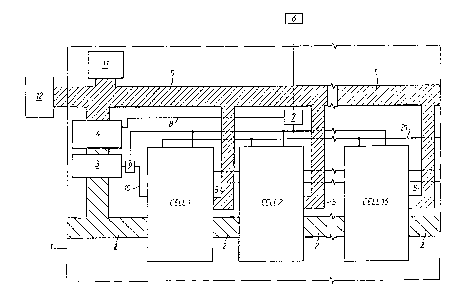
present invention which is illustrated in Figure 6 of the
drawings, relates to the alignment, or partial alignment, of
the antenna of at least two equipments 46 and 47 for the
purpose of transferring information between equipments either
unidirectionally or bidirectionally.
The equipments 46 and 47 could be independently mounted
either on a fixed body, or a moving body.
The purpose of these applications of the data processor
according to the present invention is to provide, via a look-up
table or other storage means, a position reference (which could
be, but is not necessarily limited to, star sensor
arrangements) for one or both equipments 46 and 47 to
facilitate alignment of the information transfer antenna or
antennas.
The data processor could, for example, be used to align
satellite antenna with a ground station, or with at least one
other satellite.
18
WO 95125302 PCTIGB95100312
~.~
Alternatively, the data processor could be used with the
satellite's beam former to correct for movement of the
satellite and to thereby keep the generated beam pointed in a
desired direction.
With such arrangements, the satellite could be moving in
a geostationary orbit and the correction could, therefore, be
used to increase the life of the satellite due to the fuel
savings resulting from the correction.
If the satellite is in a non-~geostationary orbit, then the
data processor could be used to aim the beam at a given area
in the sky.
If the satellite is revolving and only pointing at the
ground station, or another satellite, for a short period of
time, then the data processor could be used to correct the
'pointing' of the satellite to give a longer contact time for
information transfer and to thereby recover, what might
otherwise be, an out of control satellite, or to allow a better
contact time, if the rotation of the satellite is intentional.
A further application of the data processor according to
the present invention is in a star sensor on a satellite, for
example, the star sensor shown in Figure 3 of the drawings.
The star sensor according to Figure 3 includes a CCD array
27 having a lens 28 associated therewith which causes the light
radiating from the night sky to be applied to the CCD array 27.
The output from the CCD array 27 is connected to a data
processor 29, according to the present invention, via an
analogue to digital converter (ADC) 30 having input buffer
19
WO 95125302 PCT/GB95/00312
2~~38r8~9v
stores for the output for the CCD array 27.
The series of discrete n-bit parallel output signals of
the data processor 29 which could be in the form of two
12-bit words that are each representative of the magnitude and
relative position of the output of a pixel of the array is
27,
connected to the input of a parallel to serial converter 31
having associated therewith means for identifying the relative
positions of the data elements and means for controlling the
operation of a CCD drive circuit 32.
The drive circuit 32 causes the outputs of the rows of the
CCD array 27 to be successively connected to the input of the
ADC 30.
The output of the converter 31 which will be a series of
discrete data signals indicative of the magnitudes of the
N-highest light radiation levels detected by the CCD array 27
and their relative positions, is compared by means of a
computer with known star data in order to determine the
positions of the located stars.
The locations of the stars in different sectors of the sky
together with their light radiation values are known and are
contained in star separation tables. It is this data which is
compared with the output of the converter 31 to identify the
star field that is being viewed via the lens 28.
The data processor according to the present invention may
be used in many other applications and, in particular, systems
of the type which are illustrated, in the form of a bl ock
diagram, in Figure 7 of the accompanying drawings.
WO 95/25302 PCTIGB95/00312
~' 2183889
As illustrated in Figure 7, the system comprises at least
one data processor 49, according to the present invention,
having its input connected to a sensor unit 48 and its output
connected to the output of the system via a further data
processing unit 50 and an interface unit 51. The operation of
each element of the system is under the control of a control
unit 52. Whilst the sensor unit 48, used far any particular
application, is dependent upon the nature of the data being
processed, the main function of this unit, in association with
the control unit 52, is to detect an analogue input signal and
suitably convert each element of the analogue signal into a
digital word for application to the input of the data processor
unit 49. The output of the sensor unit 48, or the input of the
data processor 49 may include buffer storage means for storing
the digital word output of the sensor unit prior to its
application to the data processor 49. The output of the data
processor 49 is, in dependence upon the particular application
and under the control of the control unit 52, subject to any
necessary further processing by the processor unit 50, and the
interface unit 51 ensures, in association with the control unit
52, complete compatibility between the output of the system and
the input of the equipment to which the system output is
connected. The required construction and mode of operation of
the units 50 and 51, to suit a particular application, will be
directly evident to persons skilled in the art. Also,
depending on the nature of the parameters to be processed, it
may be necessary to use more than one of the data processors
21
WO 95!25302 PCTlGB95l00312
~~,83889
according to the present invention.
Thus, the data processing system illustrated in Figure 7 of
the drawings could, for example, be used to co-ordinate the
separation of two vehicles, where the separation distance is
continuously decreases in value until the interception of the
two vehicles. With such a system, the analogue signal, at the
input of the sensor unit 48, would be indicative of the
position of one of the vehicles, relative to the other vehicle,
and the output of the system would be applied to a guidance
system for the vehicles and used, as appropriate, to correct
any deviation from a desired path between the two vehicles.
For this application, the sensor unit 48 could be an
optoelectronics device and adapted to detect light reflections
from either one, or both, of the vehicles. In the case of a
laser guidance system for the vehicles, the sensor unit 48
could be adapted to detect the light reflections resulting from
the use of such a guidance system. Alternatively, the sensor
unit could be adapted to sense the output of the vehicle's
exhaust system.
The data processing system illustrated in Figure 7 of the
drawings, could also form part of a guidance system for
acquiring and homing upon a signal source. For this
application, the sensor unit 48 would not only be adapted to
sense the signal emanating from the source which could be sound
waves (for example, noise), or heat radiation (for example,
from a hot spot on an object), or radio signals, but would also
be adapted to process the collected data prior to its
22
WO 95/25302 PGTIGB95I00312
21838.
application to the data processor unit 49, i.e. it would be
necessary to interpose a pre-processor unit between the units
48 and 49 which could, in dependence on the nature of the
signal source and the collected data, be adapted to effect, for
example, fast fourier transformation, correlation, signal level
detection etc, of the input data. The output of the interface
unit 51 would be applied to a guidance control unit (not
illustrated) to enable the guidance system to home in on the
signal source.
In a further arrangement for the data processing system
of Figure 7 of the drawings, read/write data storage means
could be included to store the current state of the input data,
compare the next set of data inputs with the stored data, any
differences detected between the two sets of data being used
to effect control of the necessary elements to compensate for
the difference.
A typical arrangement for the read/write data storage
means is illustrated, in the form of a block diagram, in Figure
8 of the drawings. The read/write data storage means of Figure
8 is interposed between the units 48 and 49 of the data
processing system of Figure 7 of the drawings, i.e. the input
of a read/write data storage unit 53 is connected to the output
of the sensor unit 48 and to one input of a subtraction circuit
54, the output of which is connected to the input of the data
processor 49, and the output of the sensor unit 48 is connected
to another input of the subtraction circuit 54.
Thus, in operation, each frame of the digital output of
23
WO 95/25302 PCT/GB95/00312
the sensor unit 48 is simultaneously applied to an input of the
subtraction circuit 54 and to the input of the read/write data
storage unit 53 where it is stored pending receipt of the next
data frame. On receipt of data frame, the read/write data
storage unit 53 causes a previously stored data frame to be
applied to the other input of the subtraction circuit 54, any
difference between the two data frames being detected and
applied to the input of, and processed by, the data processor
unit 49. The output of the data processor unit 49 is used, in
the manner outlined above, to effect control of the necessary
elements to compensate for the difference. This method of
operation, i.e. frame-by-frame, whilst suitable for a number
of applications of the data processing system according to the
present invention, does not take account of the cumulative
effect of the changes in the input signal.
In those application where the cumulative effect of the
input signal variations is a necessary requirement, the system
can be reconfigured by connecting the input to the read/write
data storage unit 53, as shown by the dotted line 53a, to the
output of the data processor unit 49 rather than to the output
of the sensor unit 48. With this arrangement, the input of the
sensor unit 48 is compared, in the manner outlined above, with
the output of the data processor unit 49 thereby taking account
of the cumulative effect of the input signal variations.
The interface unit 51 of the data processing system of
Figure 7 of the drawings could be replaced by the electronic
drive and control system which is illustrated, in the form of
24
WO 95125302 ~ PCTIGB95N10312
2 ~. ~,:~
a block diagram, in Figure 9 of the accompanying drawings. A
data processing system of this type could be used, for example,
to maintain the alignment of a tracking device upon a target
by manipulating the mounting points of the sensor, or as part
of a vehicle guidance system.
For the target tracking arrangement, the blocks 55 and 56
would respectively be in the form of an x-axis drive unit and
a y-axis drive unit for the tracking device, and the blocks 57
and 58 would respectively be in the form of an x-axis actuator
unit and a y-axis actuator unit for the tracking device . Thus,
any detected deviation in the alignment of the tracking device
will cause the output of the processor unit 50 to cause, under
the control of the control unit 52, an output signal to be
applied to either the x-axis drive/actuation units 55 and 57,
or the y-axis drive/actuation units 56 and 58, to effect a
corrective change to the alignment of the tracking device.
For the vehicle guidance system, wherein the vehicle is
required to follow a path defined by a light reflective line
marked on the surface the road, or the like, the sensor unit
48 would be adapted to sense the light reflected by line
marking and the blocks 55 and 56 would respectively be in the
form of a left-hand drive unit and a right-hand drive unit for
the vehicle guidance system, and the blocks 57 and 58 would
respectively be in the form of an left-hand actuator unit and
a right-hand actuator unit for the vehicle guidance system.
With this arrangement, the sensor unit 48 could include
a single linear row of charged coupled devices (CCDs) and be
PCTIGB95100312
W O 95125302
adapted, such that, the l~i~lit reflected by the line marking
would normally causes illumination of the CCDs located in the
centre of the single row, i.e. a centrally located band of
CCDs, when the vehicle is following the correct path. Thus,
any deviation from the correct path would result in the light
reflected by the line marking to illuminate at least one of the
CCDs on one, or other, of the sides of the centrally located
band of CCDs. This would be detected by the data processor
unit 49 and would result in a signal being applied, under the
control of the control unit 52, to either the left-hand, or
right-hand drive/actuator units and to thereby adjust the
steering of the vehicle until it is following the correct path.
This vehicle guidance system can be used with multi-path
systems which run adjacent to, or cross, each other, provided
that each of the paths is defined by a line marking having
different light reflective properties to the line markings for
each of the other paths. For example, for a system having
three paths, one of the paths could be defined by a white line,
another of the paths by a light grey line, and the other of the
paths by a dark grey line. The data processor unit 49 could,
in association with the control unit 52, be adapted to provide
output signals for controlling the direction of travel of the
vehicle such that it follow a preselected one of the multi=
paths.
In mobile radio telephone systems, the radio link
established between a called party and a calling party can fade
due to signal strength variations, or, in some instances, be
26
WO 95125302 PCTIGB95I00312
218-388
totally lost. Whilst known mobile telephone systems include
means for overcoming these problems, they are not always
successful, and tend to be slow in operation.
The data processor according to the present invention can
be used, in a manner which is illustrated in Figure 10 of the
accompanying drawings, as part of a mobile telephone handset,
to detect and recognise an electromagnetic signal, and maintain
reception with another party at an acceptable level.
Furthermore, this method of overcoming the above-mentioned
problems of known systems, is much quicker, and more efficient,
than the known solutions.
In Figure 10, the electronic components of the mobile
telephone handset for determining the channel frequency for the
handset are enclosed by a dotted line 59 and comprise a radio
frequency (rf) receiver 60, a mixer circuit. 61 and a local
oscillator 62 which are interconnected, and operate, in a
manner known to persons skilled in the art. The data processor
according to the present invention is represented by the block
63. The input of the data processor 63 is connected to the
output of a multi-frequency detector 64, and the output of the
data processor 63 is connected to an input of the local
oscillator 62 via a control unit 65. The input of the multi-
frequency detector 64 is connected to an output of the mixer
circuit 61. Thus, all of the signal channel frequencies which
are received by the rf receiver 60, will be applied to the
input of the multi-frequency detector 63. The data processor
63 is adapted to monitor, in a manner as previously outlined,
27
WO 95!25302 PCTIGB95/00312
2la~g~9
the signal strength of each of the received frequency channels
and to generate an output signal for application to the local
oscillator 62, via the control of the control unit 65, either
to correct for any drift in the operating channel frequency
of the mobile telephone, or, in the case of unacceptable signal
strength variations, to change the operating channel frequency
of the mobile telephone handset to a new frequency channel
having a higher signal strength.
It will be seen from the foregoing that the data processor
according to the present invention can be used in many
different applications, some of which have been described and
others of which will be directly evident to persons skilled in
the art.
28