Note: Descriptions are shown in the official language in which they were submitted.
2184266
WO 96/20578 PCT/IB95/01106
Mrthod for ig~iting and opf -, t;ng a high-plesaulc discharge lamp and a circuit for
pc.rul.lling the mPthl)d
The invention relates to a method for igniting and OpC.~ g a high
~JlC~aUlC gas discharge lamp in particular at high frequenri~Ps, and also to a circuit for
pc rul--ling the method In general a circuit for igniting and opc ~t;ng a high pleaaulc
discharge lamp is called a ballast. In particular, the invention relates to a method which
5 deteccts arc inct~hilitiPs in the larnp and adjusts the operating frequency of the ballast to avoid
visible flicker during lamp opC~tirJn.
High pressure discharge (HID) lamps, such as mercury vapor, metal
10 halide and high pressure sodium lamps, are typically operated with a m~gr-Pti~ ballast at or
slightly above normal power line flc l~uen~;es, e.g. 50-100 Hz. It would be desirable to
provide an electronic ballast which o~ldtes HID lamps at high frequencies at above about 20
kHz. High fle.luen.;~ ballasts are be~G...h-g increasingly popular for low pressure Illcl~;ul~
vapor fluul~scent lamps. The high frequency operation permits the m~nPtir PlemPntc of the
15 ballast to be reduced greatly in size and weight as co--,~ d to a convention~l low fiequenc~
rn~gnPtic ballast. High frequency operation also provide subst~nti~l increases in lamp efficacy
on the order of 10-15% for fluorescent lamps because of re~Uctionc in cathode drop. Similar
reduction in size and weight would be desirable for HID lamps, ec~i~lly for lower wattage
metal halide lamps used for shop and track tighting, because it would provide greater
20 flexibility in decigning ~psthptir~lly pleasing fixtures for such uses. Lamp efficacy would also
increase a few percent, though not nearly as much as for nuol~scent lamps.
A major obstacle to the use of high frequency electronic ballasts for HID
lamps, however, is formed by arc instabilities due to acoustic reson~nces which can occur at
high frequency ope~ti~ ACouctic resoll~nces, at the minimum, cause flicker of the arc
25 which is very annoying to hllm~nc In a more severe case, arouctir leson~nce can cause the
discharge arc to extinguish, or even worse, stay p~ nently d~PflP,ct~Pd against and damage
the wall of the discharge vessel, which will cause the discharge vessel to eYp'~e
The frequencies at which acoustic reson7nre occurs depen~s on many
factors, int luriing the rlimPnciol-c of the arc tube (i.e., length, ~i~mptpr~ end chamber shape,
w096/20578 ~ P1842~6 PcrlIs95lollo6
the pl~ s~,lce or ~hspnc~ of a tubulation), the density of the~gas fill, opf .~l;ng te~ dlu
and lamp oripnt~tinn- For high frequency b~ ct~ th`e operating frequency of the larnp
current fI will gPn~Pr~lly be se~ to be above the audio range (fI > 20 kHz), but may be
lower. For the typical ballast op~ g with (distorted) sine waves, the power frequency fp is
S twice the frequency of the current, so fp will be greater than 40 kHz. The arc tubes, or
discharge vessels, of high pl~,Saulc; sodium lamps and some of the newer metal halide lamps
are cpr~mic and cylin~rir~l in shape. The arc tubes of Illtll.;UI,~/ vapor and metal halide
lamps are made of quartz glass, typically with a cylindrical body and rounded end rh~mb~prs.
The power frequencies at which longitll~iin~l acoustic reson~nre occurs for these generally
10 cylintlrir~l arc tubes can be app~ t~d from the formula:
f"= n 2~ ~ n=1,2,3,......... (1)
where L stands for the typical length of the arc tube, n denotes an integer number, CL
denotes an averaged speed of sound in the length direction of the burner and equals
applu~Lh,,ately 450mls. The radial-~,;...ull.~l modes are given by:
fb~ ~h 2rI~. (2)
15 where Cr denotes an averaged speed of sound in the radial direction, R denotes the typical
radius of the arc tube, and CYIm denotes the zeros of the first derivative of the Bessel
filnrtiQnc
The complete reson~nre ~e~ u"~ f~mr~ is c~lcul~tP~3 from:
fL~ (3)
If the length of the arc tube is sllbst~nti~lly larger than the radius, the frequencies at which
20 flicker occurs can be estim~tP~d from formula (1) for longitu~lin~l resonallt frequ~Pnri~s
For the specific case of a lOOW metal halide lamp with an arc tube length
of lS mm, for e~mrle, the lowest longihl~in~l resonallt frequencies are ~ d to occur at
power frequencies of 15 kHz. Therefore, higher order reson~nrPs will occur at power
frequencies fp above 30 kHz, which coll~spond to current fic~luer~- ;es fI above the audible
2184266 :
wo s6/20s78 ~ IBsslollo6
range.
Thus, the resonant frequencies can be approYim~t~d by c~lr~ tion and/or
observed through e ~ cnl~ by op~ . . t;,-g the lamps at varying frequencies and visually
observing the reslllting flicker. For a specific larnp type under specific Opf'~ g Con~itiQnS,
5 an opf ~.I;ng rlc luency can be c~ l~ at which visible flicker does not occur and a ballast
d~PcignP~ to operate the lamp at this pre-selP~tP~ frequency. However, the ballast would be
lirnited to a crerific wattage larnp of a specific m~mlf~rtllrer. Furthc..,-o~e, ch~nging
op~ -l;.-g con.litif nc such as ch~ngin~ environm~nt~l conflitif~nc or larnp bl~r~ ~ing over
life, which would alter the o~ .~;ng ~,.,l~ 1tu,c and/or ~.es~us~, could change the l~sondl t
10 frequencies so that reSQn~nre occurs at the pre-selP~te~ balla t oF~.Anng fic~uenc~.
~ n~tively, ecreri~lly in the case of quartz glass arc tubes where ~ c~ l control is
~iffit`l-lt even lamps from the same manufacturer would have difr~.~, t lesonant points so
that it is possible that a col~ci~P~ble pclcer~dge of lamps would flicker at the sel~t~P~d ballast
operating frequency. Besides not being fault free, manufacturing a ballast for a specific lamp
15 of a certain m~mlf~rtllrer is expensive in view of its limited market and is inflexible for the
user. Accordingly, it would be ~ecir~hlP~ to provide a ballast for a broader range of lamps
which senses arc in~t~hilitiPs during operation and selects the op~ ;ng frequency to avoid
arc instabilities due to acoustic reSon~n~e
The article ~An Autotracking System For Stable Hf Opçr~tion of HID
20 Lamps", F. Bernitz, Symp. Light Sources, Karlsruhe 1986, dicrloses a controller which
continuously varies the lamp opeldting frequency about a center frequency over a sweep
range. The sweep frequency is the frequency at which the ope.d~ing ~l~u~nc~ is l~atced
through the sweep range. The controller senses lamp voltage to evaluate arc instabilities. A
control signal is derived from the sensed lamp voltage to vary the sweep ~.~u~n.;y bcl~cen
25 100 Hz and some kHz to achieve stable op~r~tion~ However, this system has never been
commPrci~l j7p~
JP 4-277495 (Kamaya) diccloses a ballast which senses the i~re~nce of
the discharge lamp. If the i...pedance of the lamp is below a sI~esifiP~ level, the ballast
reduces high frequency oscill~ting co---ponenls in the lamp current. A disadvantage of this
30 design, however, is that the s~ifiP~ level is fLxed, and as noted previously, the ~sonanl
rl~uencies in reality vary from lamp to lamp. Ad~litiQn~lly~ even though the high rl~u~nc~
co~ Qn~r.t<i are reduced in the lamp current, there is no gu~ that op~tinn will not
shift to another l~sonant f~ uenc~ at which arc inct~hilitiPs occur.
Accordingly, it is an object of the invention to provide a method of
2I84266
wo 96/20578 ~ PcTlIssslollo6
detccting arc jnct?~ilitiPc in gas discharge lamps, which is universally applicable regardless
of lamp power, type, dimpnci~n~ or physical or chemir~l co...l-os;~ n It is another object to
provide such a method which may be implc ~-~ r,~A in a~wide range of ballast tnpolcgiPs
It is yet another object to provide a method of ope.~;ng HID lamps at
5 high ~r~u~ncies to detect and avoid frequencies at which acoustic ~SOn~l~C~ occurs for a
broad range of lamps, or at least lamps.
It is still another object to provide a lamp ballast, or controller, which
impl--nPnts this method
In the method according to the invention, arc inst~hilities are del~l~ by
ev~ ting the deviations in an elP~trir~l p~r~mçtPr of the lamp. The lamp Opf.r.l;i-g
p~r~m~ptprs can then be changed based on an ev~ln~tion of the deviations to avoid further arc
instabilities. The invention is based on the recognition that arc instabilities are acco~p~n;~P~d
15 by defo~ t;rlnc in the arc which change its length, which in turn vary the elP~tr
p~r~m~Ptprs of the lamp, such as the voltage, current, con~lucl~n~e~ or inversely, the
i...p~PA~nre of the larnp. Ope~ting frequencies at which arc inct~hilitiPs occur caused by
acoustic reSon~nre are determined by ev~ ting the de- iations de~ ,ined at each of a
plurality of OpC.d~ g frequPnriPs
An embo~limtont of the invention particularly suited for detecting the
frequencies at which arc inct~hilitiPs occur due to acoustic resol-~nre inrllldes the steps of:
operating the gas discharge lamp at a plurality of frequ~Pnries; sensing and taking a plurality
of c~mphPs of a S~PlPot~pA- el-pctric~l p~r~mpter at each frequency; c~lc--l~ting a deviation, at
each of said plurality of frequenci~Ps of the ~mpl~Ps of the Pl~t-ir~l p~ -.,PI~r taken at each
frequency; ev~ ting the c~lrlll~tpA deviations; and selP~ting a lamp op. ldLing frequency
based on the evaluation of the deviations. Favorably, the deviations are evaluated to
determine the frequency having the lowest deviation in the ~mplçd lamp parameter and the
ope,d~ing frequency is set at this frequency. TtP~ting the above-steps with dirr~..t rl~u~ n~;y
spans and scan rates enables the frequencies at which the global and then local .~ lllls in
30 the deviations and thus in arc dPflP~tion~ occur to be rapidly and ?sc~ ly dc~ ined.
Favorably, the lamp p~r~mPtpr sensed is the conduct~nce or the
nre, which in general permits the ~rcnr~tP det~P~tion of much smaller arc rleflPoti
than is possible with either voltage or current alone. By eV~ ting deviations in the
c~nduct~nre, it has been found that arc dPflPctions due to ~roustir l.vso~-~nc~ can be sensed at
wo 96/20578 21 8 4 2 6 6 ~Cr/IBsslollo6
levels which are not pef~lible to the human eye. The use of conduct~nre or i~"peA~nr~
which are ratios of the lamp voltage and current, permit simpler c~mpling techniques than is
pocciblp with either the voltage or current alone. Ad~ition~lly, use of the co~luct~nr~ or
i..,~ce ove.~",cs the problems with sensing voltage or current alone, which generally
S does not work prope.ly. For Py~mple~ voltage detP~ctinn alone is sensitive to line v~n~tinnc
such as surges, mains dip and other eYtPrn~l con~itionc.
According to another Pmhot~imPnt, the deviation detP~tPd is the ~ d~.l
deviation. This has the advantage that all deviations of the arc detP~tPd in a ~mplin~ interval
contribute to the effective deviation rather than, for inct~n~e, only the ,.~ .. deviation
10 dete~ted in a ~mpling interval.
According to another embodimPnt, the det~ction of the frequencies at
which ~rouctic resc~n~nre occurs is ~rcomplichPd by coll~ucting a symmPtrie~l sweep of
fl~quencies about a center frequency, the sweep inclu~ing a portion with a set of frequencies
wherein the frequencies are increasing and a portion inrlu~ing the same set of frequencies
15 wherein the flc~lu~ncies are decr~asing. It was discovered that there is hysteresis in the
defl~P~tion l~pOI-cP~ of the arc, so that the arc dçflertionc at any given frequency are
depend~nt not only on the sweep rate at which the frequencies are changed but also on
whether the frequencies are decreasing or increasing. By m~cllrin~ the deviations at each
frequency in a s~ e~ ;c manner, i.e. c~mpling at each frequency both when the frequencies
20 are increasing and when they are decreasing and at the same sweep rate, the effects of
hysteresis are Plimin~t~d and deterrion of the frequencies at which reson~nce occurs is
improved.
Favorably, the det~Pctio~ of the flicker-free frequencies and sPl~ti~n of
the opelati.lg frequency are conductçd during a run-up stage of lamp operation, between
25 ignition of the lamp and steady-state operation. In the run-up stage the frequencies at which
acoustic l~n~nl~ occurs rapidly changes due to the increasing gas pressure and t~ pf~
of the lamp. While this does not immPAi~tPly appear to be a good environment for ~etPoting
the frequencies having no visible flicker due to ~r-o~stir reSon~nr~ it has been found that the
frequency sweep and iteration speeds can be selP~tPd so that a controller can home-in on a
30 frequency with a local minimum in the deviation of arc deflection and track this miniml)m
through the end of run-up. This has the advantage that when the run-up period is over and
the lamp has reached full light output, a desirable opel~ g frequency has already been
sele~l~d and the lamp can be opc.ated with no visible flicker as early as the end of the run-
up period. This technique has been found to work well despite the lower possibilities of
w0 s6/20s78 21 84 26 6 Pcr/Isss/01l06
developing arc inct~hilitiP5 during run-up due to the lower gas ple.~Ul~,S and ~...~ S.
Favorably, the d~PtP~tinn of deviations in the arc continues during steady state opçr~tinll so
that adjusn.. .-lc can be made in the Opf.~ g frequency~t~o~coinnt for small ch~ngçs in the
gas fill p~,S~ulc and/or tclllpcl.~lulc caused, for example, by environmPnt~l effects. For
5 control in the steady state, the span and sweep rate of the ficL~uenc~ sweeps are CflP~d so
that visible flicker is avoided.
Random dPflp~tiQnc in the arc can occur due to effects such as arc jumps
at the electrode or flare-ups caused by droplets of the fill m~tPri~l in the lamp discharge
vessel suddenly entPring the arc stream. If these random events are not ~rc~u.-l~f-~ for, they
10 would cause errors in the detP~tinn of the standard deviations during the r~u~.lcy sweep
and cause operation at a new fiequ~lcy cGlle~l.ol-~ing to a false l--ini-------- in the standard
deviation. In order to avoid this, in yet another cmbo-1imPnt, each frequency sweep is
conductPd twice concp~utively and operation at a new center fi~qu. ncy is begun only if the
difference between the respective set of deviations measured in the two itPratin~lc are within a
15 prescribed level.
The lamp controller, or ballast, according to the invention inrlt~des a high
frequency inverter for opeldLng an HID larnp within a splf~tpd frequency range. The
inverter is responsive to a control signal supplied by an arc instability controller which
i,.lple...enLs s~lf~l~ steps of the above-d~Pscrihed mPthod In an embo~limpnt~ the arc
20 instability controller inrludPs a mic~oproceçsor progr~mmPd with sofLwalt to carry out the
sel-P~t~Pd method steps.
In contrast to known commercially available systems, the ballast employs
universal opeldtiilg principles suitable for operating HID lamps of different types,
m~mlf~cturers and wattages despite the occurrence of acouctir resnll~nre among ti ese lamps
~5 over a fairly broad frequency range.
In a favorable embo~iimpnt the baLlast inrlud~ps a control device which
ensures that the power delivered to the lamp remains s.~bst~ lly conct~nt despite changes in
the inverter frequency, and consequently the lamp Opc~aLtng frequency, during dete~tinn and
avoidance of acoustic reson~nce In order to ensure proper lamp operation, the power
30 delivered to an ~D lamp must be kept within a fairly narrow range around the lamp wattage
rated by the lamp m~nuf~rtnrer. V~ri~tinnc in the lamp power will change photGu.ehic
parameters such as lu~-linous efficacy, light output, color ~IIIl~-AIlllc; of the emitted light and
color rpn~pring~ which is nn~Pciral-lP Accordingly, with this measure, ~Ouctir l~ n~n~4
detP~tinn and avoi-l~nf e is carried out by the ballast, particul_rly during the steady state, in a
Wo 96/20578 2 1 8 ~ 2 6 6 ~ ~ PcT/Issslollo6
manner ~lb~ n~ ly invisible to the user, i.e. subst~nti~lly without visible flicker and
bs~ lly without visible ch~ngps in light quality and in~nsil~.
In an e.llbo~ nt of the ballast, the power control is oblained by
controlling a bus voltage output of a boost converter which feeds the inverter. The gain of
S the inverter circuit, and cons~u~"tly the lamp current, is dependPnt on the inverter
frequency. Lamp voltage and current are sensed to obtain a lamp power signal, which is
co.l.paled to a reference power signal. The duty cycle of a boost switch in the boost
converter is controlled to adjust the bus voltage to compensate for ch~ngPs in the gain of the
inverter. Since the power control limits the power, it also serves to pl~rent cat~Ll~hic lamp
failure at end of life.
In yet another embo~iment the ballast inrludes a control for cl~mping the
bus voltage during lamp ignition and run-up, when the lamp ~,r~ser,ts only a very small load
to the boost converter, to protect the circuit elempntc and lamp.
These and other objects, featules, and advantages of the invention will
15 become app~c;,lt with reference to the drawings and following det~ilPd decrrirtirJn, which are
ill,.ct~tive only, and not limiting.
Figure 1 illnctr~tPs a rlicpl~remPnt of a flirl~Pring discharge arc;
Figure 2 illustrates a favorable sampling technique for mP~curing the
standard deviation in conduct~nre within a frequency window;
Figure 3 is a flowc},~L of an Open Loop Control for finding the minimnm
flicker in a sel~rt~d frequency interval and r~lrul~ting the standard deviation jc from
con~urt~nre sa--,l)les Gjk, according to one embodimPnt;
Figure 4 illustrates a simultaneous s~mpling of voltage and current for
r~lrul~ting conduct~nre;
Figure Sa illustrates a global frequency sweep for detecting strong
reSon~nres;
- Figure 5b illuctr~t~s the ln~c~tion of strong ~snn~nces and of permiccihl~
30 ope,~ g windows which are free of strong l~son~nr,es;
Figure 5c is a chart of the permiccihle opr ,~l;ng windows at which strong
reson~nces do not occur for several different 100W metal halide lamps A, B, C, D, E from
different manufacturers;
Figure 6a illustrates the deviation in cQndurt~nr,e ~pl~sen~ g weak
wo 96120578 2 1 8 4 2 6 6 ~ Pcrm~s~/01l06
8 - ~
reson~nres over a range of ~l~u.,ncies within an~allowable window of Fig. Sc;
Figure 6b ill~ctr~tP5 the global minimllm for weak ~c~n~n~s, in the
standard deviation of the con~lucl~n~e shown in Figure 6a;
Figures 7a, 7b and 7c illuctr~te three control options for detP~ting the
S global ..;n;--.--... in the ;,~~ d deviations for weak reson~n~ps;
Figure 8 illllctr~tps the deviations measured around the sPIected Opf~al;llg
rlequer,c~ in steady state ope~tinn;
Figure 9 is a flow chart of a control loop for opc~,~t;ng a high pfeS~
discharge lamp;
Figures lOa; lOb show the output of the routine of Figure 9 for a lOOW
metal halide lamp;
Figure lla illuct~tPs a citll~tion where standard deviation a has a broad
and a narrow ...;n;..-l--.- both lower than a boundary value afl;
Figure llb illnctr~tPs the splpctinn of the broader minimllm as the new
lS global minimum from the smoo~hed data of the standard deviation a;
Figures 12a; 12b illustrate le~lesenta~i./e con~-lctivity recponc~Pc for arc
deflP,ctionc caused by arc jump and sodium flare, respectively;
Figure 13 is a block\crhpm~tic diagram of an HID lamp ballast with
reson~n.~e detectinn and frequency control;
Figure 14 is a s~h~ ;c ~i~gram of a power and bus voltage control
(Control D) of Figure 13;
Figure 15 i~ stratps a pulse width control of a control signal Vgsl for the
boost switch Ql to control the bus voltage and the power delivered to the lamp;
Figure 16 shows the circuit connP~tions of IC's embodying the various
el~pmpntc of Control A and Control D of Figure 13;
Figure 17 is a block diagram of Control C of Figure 13 for Arc Tnct~hility
Control; and
Figure 18 is a schr~ rii~gram of a half-bridge controller (Control B)
of Figure 13.
Figure 1 illustr~tPs a discharge arc 1 between a pair of discharge
electrodes 2 of an HID lamp in a vertical op~ldting position. The arc tube is not shown for
the pull~ose of clarity. The arc is subject to flicker in~uced by ~-~o~sti~ fer~on~n~ The center
position of the discharge arc 1 f~l~senls the poCitio~ of the arc at an ~billdl,y time t at
wo g6/20s78 2 1 8 4 ~`6 6 PCr/Is9slollo6
which it has a length L. The discharge arc at an offset position 1' shown in dashed lines
se~,~ the dPfl~t~d pocition of the arc at a time t+ ~t, from which it is seen that the arc
has a longer length L+ ~1. The dirf~nL lengths of the undefl~t~ and the defl~t~d arc
cause the e~ ;r~l lamp p~r~mett~rs, such as voltage, current, cQnduct~nce and ~ e~nc~e to
5 have different values in each of these p~sitinnc and is the major cause of change in these
el~t i~ . Thus, acoustic ~son~n~ e causes changes in the arc length and
consequcl,Ll~ changes in these el~trit~l parame~ers. Dete~tion of ch~ng~c in these p~u,-cters
thcl~fol~ gives the poscihility of det~ting acoustic reson~nce elP~tric~lly and of developing a
scheme to evaluate at which frequencies resnn~nce and arc defl~tinll occur and of
10 controlling the o~.~ing frequency of the lamp to operate at frequencies at which visible
flicker does not occur.
It should be noted that in some citll~tionC ~ticf~tory control may be
ob~ned by dete~ting deviations in only the lamp voltage V or the lamp current I. However,
using the i~ nre and, in particular, the conduct~nce G=I/V has numerous adv~nt~gPs
15 Measurements of the change in conduct~n~e or impedance will always have an equal to or
better signal-to-noise ratio than measurements of the change in the current or voltage only.
The signal-to-noise ratio is typically 20dB higher in the conduct~nce or the ~ e~l~n~e than in
the current or voltage alone. By ...~c... ;.-g both voltage and current simlllt~n~ously to
c~l~ul~tP their ratio for the imre~nce or conducPnce, noise contributions, for eY~mrle from
20 a power line, in each of these signals subst~nti~lly cancel. If the voltage or current were used
alone, these noise signals would remain. These advantages enable detection of very small
deflP~tionc in the arc which are not noticeable to the human eye and which in practice are
typically not dete~t~hle using lamp voltage or current alone. ~d~lition~lly~ control based on
conduct~n~e or i..-~ n~e is in~Pp~nd~nt of circuit topology of the lamp controller whereas
25 control based on voltage or current alone is topology dependent Finally, when both voltage
. and current are sensed cimlllt~n~ously to calculate impedance or conduet~n~ a much simpler
sampling scheme may be used than is possible with sampling voltage or current alone.
While detection of the i..-pedance or conduct~nre share the above
advantages, detection of the conduct~nce is p~efell~d for the reason that, before, during and
30 imm~Ai~t~.ly after ignition, the lamp current is zero or very small and the lamp starting
voltage is very high. During these inct~n~es~ the impedance R=V/I would be infinity or very
high. Conversely, the con~uct~nce G=I/V is zero or small during these periods and can
always be ç~ t~, Using the conduct~nce also makes the m~thod/ballast less sensitive
towards the lamp. For example, if a lamp is replaced or subsLiLuLed with a different lamp
218~266
wo 96/20s78 PcrlIs95lollo6
type, V and I will change but G = V/I willtremain in the same relative range. With the
conAuct~nr~, this control can be c~nciAPred even more universal, i.e., can be applied to a
variety of lamps of dirr~,e.lt type, make, and wattage. Accordingly, throughout the
rem~indPr of the det~ilPd description the embo~imPntc will be described with reference to
5 dete~tinn of the cnnAuct~n~e, and those of o~lin~ y skill in the art will appreciate that the
impeA~nce could be subctitutpd in the following embo~impntc so long as ev~ tif~n in the
first few se~onAC after lamp ignition is avoided. Addition~lly, those of o~ s,y skill will
appræiate that, where the signal strength of the voltage or current is s~ffi~iPntly high to
obtain c~ticfactory control, c~mrling of the voltage or current alone may be used instead of
10 the conduct~n~e
The method and baUast according to the invention employs several phases
of control, each of which depen~s on the sampling of conductance at a plurality of
frequencies and the c~lrul~ti- n of a selP~t~Pd deviation at each frequency. Accordingly, a
favorable conduct~nre c~mrling and deviation calculation technique will be d~Pscrihed prior to
15 ~iccuccing the phases of control.
Calculation of Conductivity fSamplin~)
The task is to c~lcul~te the conduct~n~e g(t) from the rapidly ch~nging
voltage and current. For an HID lamp opeldting on a typical high frequency ballast with
20 distorted sine waves, the lamp voltage is a periodic alternating function V(t) = V(t+p) with
a period p = 2~1Z). In case the current frequency fi and thus the voltage frequency are above
the audible range, i.e. above 20 kHz, then p < 50~s. The current by definitiQ~ is given by
I(t) = g(t)V(t). The conductivity or cond~lct~nre g(t) is only a slow ch~ngin~ positive
function of time, almost conct~nt during an appropliately chosen sample time T. At least two
25 samples are taken in the period p (to avoid dete~ting small signals only), and during a certain
time T > p (on the order of ms) a total of N samples are taken. By definition~ we will
collsidP~ the values G:
where in general <f> denotes by dPfinition the averaged value of observed values fi, i= 1,
30 2, ... N:
G= llVII . (4)
w096/20578 21 8q266 11 PcrlIssslollo6
<f~ f, (5)
i-l
Absolute values in the sums for the conductivity c~l~ul~tion are taken to avoid a sum equal to
æro, and also to obtain a m~Yim~lm value of the sum (an ~lt~rn~tive is to take G = [< I2>
/ ~ V2 >]'h). S-,l s~ n of the definitionc and the equation for the current leads too:
G ~ i-l lIil ~ i_18ilVil ~ g ~ ~ i-l
~i_llVil ~i llV~I ~i_llVil
S while as ~csumed the values gj are almost conct~nt during the sample time T. When the
current and voltage are ~mple~ at the same time the two S~ l;onc over Vi cancel. This
can be accomplished very simply in practice with a simlllt~nr~us sampling board. It is not
n~ec~. ~ to sample an integer number of periods p, because the ~.,...,.~t;~nc are always over
the same c~mrles Vi.
To detect ~ro~lstir reson~nces, the general scheme is to operate the gas
discharge lamp at a plurality of frequenriPs, at each frequency c~lr,l~l~t~ the conduct~nce a
plurality of times by taking a plurality of cimlll~ eous s~mples of lamp voltage and lamp
current, and for each frequency c~lcul~te the standard deviation of the conduct~nres taken at
that frequency. This procedure is notionally given by the following equations:
fjtl j = l'~,..NG; k = 1,2,..Nf
~ i=l lV~tl
Gt=N--~,Gjt, k = l,.. NF, ot2 = N--~,(Gj~ - G,t)2 = ~ G,2~ - G" (8)
By taking at each frequency fk a number of NIV X NG C~mP1'S (j=1 to i=NIV; j=l to
j=NG), a standard deviation ak is detennined All samples used to c~lrlll~tP ajC are C~ t~
w096/20578 218~26 ~ PcT/Iss5lollo6
I2
at the rlc~u~.ncy f~c~ Then the next rlcquency fk is sel~ted and the c~mrling and r~lr~ tinn is
repe~t~d The frequency having the ~m~llest standard deviation is the frequency with the
lowest arc defl~tinn caused by ~-ousti~ leson~n~e and thè~frequency(s) with the highest
standard deviation(s) are the frequencies with the largest arc deflP~tinn
S A s~mpling scheme employing these equations is ~ Ct~t~d in Figure 2. A
I-;r rl~u~ncy sweep over a sequence of frequencies (k=0,1,2 ... 20) is cc~nduct~l. At
each frequency fk, a sequence (j=1,2 ... NG) of conductivities Gj are del~ -..;nf~d by
mr~cllring for each conductivity Gj simult~neoucly sele~t~ ~mples Ij and Vj. This is
ill.l,ni.t~d in Figure 2 for the frequency of k=2. The frequency sweep starts at a center
10 frequency fc~ decreases (portion A) to a minimllm frequency fa, increases (portion B) to a
.... frequency fb, and then decreases again (portion C) to the center frequency fc .
Portion B has the same set of frequencies as portions A and C combined. It is desirable to
sample the con~uct~n~e with the frequency both increasing and declea~ing because of
hysteresis in the deflPrtir n response of the arc. By con-lucting the frequency sweep in this
15 manner, the effects of hysteresis are elimin~t~ The span of the frequency sweep is the
difference between fa and fb. The scan rate is the rate at which the frequencies fk are
changed.
In equations 7 and 8, the indices i, j and k used at the current and voltage
inrii~tP that in prinriple these are three ~im-on~ n~l arrays. For implemPnt~tirJn in a lamp
20 ballast it would be advantageous to avoid having to provide memory for storing these values.
For the general case, the standard deviation is defined by:
N
a2 = 1~ (Xi - X~2 (9)
However, after squaring the term after the summ~tion in equation 9 and subsl;lu~;ng equation
(9a),
l N
where x = N~ Xi (9a)
25 equation 9 be~o,..fs
By using equation 10 (where xi = Gk), the calcul~tion of a standard deviation a~c of the
w096/20578 2184266 PcrlIB95/01106
13
a2 = _~ Xi2 ~ ( 1~ x)2 (10)
cQnduct~n~Ps Gl~ c~mrlpd at a frequency f~ can be carried out in software without having to
store all of the current and voltages for each sample in an array. A flowch~l for
accomplishing this while carrying out the frequency sweep shown in Figure 2 is shown in
Figure 3.
By using the con~lucPnre, the c~mpling scheme for de~c .. ;ning the
standard deviations is greatly cimplifiP~ as compared to using the standard deviation in the
voltage or the current alone. This is illllctr~tP~ in Figure 4, which shows a voltage V and
current I wavefo~ln with two sample periods i and i+l, with the arrows l~5~..t;ng the
loc~ti~n and ~mplihlde of the C~mp]es taken. In Figure 4, the c~mpkPS in period i are taken at
10 different lor~tionc with respect to the phase than in period i+l. Thus, ~¦I¦ or ~¦V¦ in
period i is not the same as in period i+l, so there would be an error in the c~lrul~tinn of the
standard deviation in the current or the voltage alone. If only the voltage V or current I are
sarnpled, the sarnpling must be triggered at the same instant in the waveform of the voltage
or current for the standard deviation to be ~cu~tP. This would entail :~riitioll~l sensing and
15 triggering devices in a ballast controller employing this technique. Such triggering would also
introduce an error into the standard deviation c~lcul~tion. By using the con~luct~nre, the
voltage and current need only to be sensed cimnl~nPoucly. The values of the simlllt~nPoucly
sensed current and voltage are norm~li7P~ in the ratio I/V which defines the con~uct~n~e so
the instant at which the c~mrlPs Gj = S IIVI are taken with respect to the sensed waveform is
20 irrelevant. This simplifies the s~mpling scheme and its implPmPnt~tinn in the ballast.
The d~PflP~Ctinn of the arc between the ele ;I,udes due to a force, induc~d
for inct~r~ce by an acoustic reson~n~e, can be described by a second order dirr~ ial
equation in time. A typical time conct~nt of ~=50ms describes the time to achieve a certain
deflP~tion. This time was detel~JIined by d~PflP~ting the arc in a 100 W metal halide lamp
25 with an external ele~;~ru...agn~tic force of known value and duration from a coil pocitinnpd
around the lamp. The equivalent force on the arc caused by an ar~u~ res~n~n~e can be
described by F=Fo sin(2~r~`ft). With this force, the highest l~,pQn~e is observed at a
frequency of ~f=3Hz. At higher ~u, ncies of the force, the frequency resp~ncP drops by
W 0 96120578 21 ~ 1~ 6 ~ PC~r~lB95/01106
14
40dB/decade. Dep~nrting on the strength of the force on the arc the defl~inn will be either
big or small. In ballasts which use a sine wave current to drive the lamp, some lc;son~nrf ~
can deflect the arc against the wall of the arc tube. Such a reson~nre is defined herein as a
strong reson~nce All other resQn~nres not able to deflect the arc against the wall are defined
5 as weak res~n~nres In order to provide a control scheme to prevent a strong rcso~ r~ from
driving the arc to the wall, the control should respond much faster than 50ms and apply a
difî. .~nt o~"~l;n~ frequency at which strong reson~nres do not occur in a time much less
than 50ms. In me~ ring flicker due to weak ,eson~nces, a time at least on the order of 150
ms should be used. Strong l.son~nees are il~lpol~Lnt in that ~lefl~Sion of the arc to the wall
10 may cause lamp esplosion. Weak rçson~nces are important in that they cause flicker of the
arc which is very annoying to hnm~n~
Lamp Characteristics
An underst~n~ling of the run-up of the lamp, i.e. the first few ~..;n.~t~ 5
15 after lamp ignition~ is il"~-~lt in developing a control scheme for the lamp. This is
~ "l.~t~ in Table I below.
WO g6/20578 21 8 q 2 6 6 PCT/IB9S/01106
TABLE I
i.,c,easing ~e."pe.al.lre -- ~,I,any;"g frequencies
t; = Os to ~ 305 t~ dy -- 1 20s
t
(T = 300K) ~T~ 5000K)
Ip = 0.3bar) i".,ftasi"g pressure Ip - 15bar~
low pressure de ,easi"g da",pi.. g high pressure
no acoustic i"c,easing i"lcnsil~ of acoustic
res~ ~a"ces acoustic resonances resona"ces
w096/20578 ?,'~,84266 ~cr/Issslollo6
16
Before igniti--n, the p~S~lc p in a typical 100 W metal halide lamp equals about 0.3 bar.
During run-up, the o~l;ng pl~ re inc,~ases towards the steady state op~ g ~ c~ cof about 15-20 bar, typically within about 120-200 seconds after ignit~ ?n. The dAmring in the
fill gas, i.e. the recict~nre to induce an ~r-oustis reSonAn~e~ and therefore the change in
5 po~citinn of the arc, is inversely plo?<jllional to the prc~ rc, so the d~mring decreases by a
factor of about 50 during run-up. Consequently, the intcrlsily of acoustic resl nAn~Ps and arc
inCt~bilitiPs inclc~es. During about the first 30 seconds after igniti-~n no Ar4Uctir le~nAnc~s
occur because it is still ecc~nti~lly a low ~ l.IIC discharge lamp. Thus, det~tion of
resonAnre and flicker through meas.llcl,lent of the conlluct~nre can not feasibly take place in
10 this time period. During further run-up, between to at ~30s and tSt~eady at 120s, the gas
cont~nt and therefore the l~sonant frequpnrips~ rapidly change due to increasing larnp
tC.~.Pe1dtUre TL, lamp fill plcs~ c~ speed of sound c, and entry of the metal halides into the
arc stream. The lo~tion of the resonant frequencies will not stabilize until the larnp has
reached the steady state at tSIeady~
If a ballast which could operate HID lamps over a broad range of rated
Wattages (2WOOW, for example) were desired, detection of deviation in the co~duct~nre
could be used to locate for any HID larnp an opcld~ing frequency which would be free of
visible flicker induce~ by acoustic reson~nce In practice, such a ballast is not commercially
practical because voltage across and current through electronic devices determines cost; so
20 each lamp is opeldted the most cost effectively by a ballast decign~d for that m~lrimllm
power. It is s~fficient~ and would be a great improvement over the art, if a high frequency
ballast could operate lamps having arc tubes of similar shape (e.g. from different
mAnuf~rtllrers) and a narrow range of wattages. A favorable emhodim~nt of the invention is
based on the pre-selection of a relatively narrow window of ope.d~ing frequencies at which
25 strong reson~nces (that cause deflertion of the arc against the arc tube wall) do not occur for
the intenrled range of lamps desired. After lamp ignition, the method and ballast
implemPnting this method operate within the pre-sçlected window to home-in on a frequency
at which visible flicker caused by weak reCon~nces does not occur for the specific larnp being
controlled. Ad~lition~lly~ since environm~nt~l contlitionc or other factors may change the
30 acoustic reson~nre nodes of the lamp, the method and ballast continu~s det~tion and
monitoring throughout lamp operation to prevent the lamp from wandering into ~oustir-
resonAn~e.
The above techniques will be explained in general terrns with lcfc~ nc~ to
w096/20578 2t ~66 PcrlIBsslollo6
- 17
Figs. 5-7. These figures illllctr~tP the dC~ n of strong ~son~nr~s and of weak ~son~nces,
both during run-up and during the steady state. A specific control algo~ ,-, carrying out a
favorable e -.ho~;.--- nt employing these techniques will then be tlicrllc~p~d
S Detection of Strong Reson~ces: Window Pre-selection
The rrc lu~nc;es fi at which acoustic lrson~n~`e occurs are at a plurality
of nodes given by Equation 3. These rlc luulcies can be confirrned through ~ f 1~ by
varying the o~,dling, or center, rl~u ncy fc over a broad range fa to fb (see Fig. Sa) at a
plurality of frequencies fk and by c~k~ul~ting the standard deviation of the con~luct~nres by
10 taking a plurality of cimull~nf~ls ~mrlPs of lamp voltage and current at each frequency f~c~
as rlicruccpd above with respect to Equations 7, 8, 10 and Figure 2. From this s.~nnillg~ the
frequencies at which strong rÇson~nres occur will become apparei1t because these rle lu~ncies
will have the highest standard deviation, and can also be visually observed. These
frequencies are shown as dots in Figure Sb.
In orda to avoid darnage to the arc tube, strong reson~nces should be
detectP~ by an iterative plUCc lul~, as ill~ ted in Figure 5b. ReC~cp of l~mping~ and the
second order ~eflPctinn ~,~once of the arc, arc dçflecti-n will be the least at high scan rates
and the glealeaL at low scan rates. If a low scan rate is used initially, there is the danger that
the arc will be dPfl~tP~ against the arc tube wall sllfficipntly long to damage it. Th~lcrulc,
20 the first frequency sweep should use a high scan rate of about 1000 kHz/s and will reveal
frequency windows at which the aLlonge~l reson~nces are observed without ~1~m~gjng the arc
tube. These ficquencies should be avoided in further scans. The frequency sweeps should be
repeated with a succ~Pccively lower scan rates of, for eY~mple, 100 kHz/s and 10 kHz/s. This
will reveal the frequencies at which the strongest reSon~nces occur. For each scan rate of the
25 frequency sweep the range of frequencies over which the center frequency fe is varied is
shown in fig. Sb by a line in~ir~tP~ with the resyeo~ e sweep rate. Windows of frequPn~s
having a span of a few thousands of hertz, at which strong reSon~nres do not occur will also
be observed and are ill--~ t~ in Fig. 5b, in the line labelled R, as solid lines. These
windows are the frequencies at which the larnp should be operated to avoid strong
30 reson~nrPc~
This plUC~ulc is either used in the larnp ballast, or by the ballast
decignPr in pre-selPcting a wide frequency window for the lamps intPnd~Pd to be controlled by
the ballast. If done by the ballast desigr~Pr, this ~-ocedule should be ~eated for each larnp
that the ballast is intenrled to operate. A cornmon window may then be se1~ted in which
wo s6/20s78 2 1 8 ~ 2 6 6 PcTlIss5lollo6
18
each of the int~nded lamps can be op~ Ated by the sarne lamp ballast without the OC~;U11~.nCe
of strong l~son~nc~s A chart of the permissible opeldLing windo~s for several 100 W metal
halide lamps A-E, each of a dirrcre,.~ m~nuf~ctllrer, are sh~own as solid lines in Figure Sc.
The common permissible OpcldLillg window in this chart i's`àt 20-25 kHz.
It is not neC~ for the pre-selected window to be complet~ly free of
strong reson~n~s The danger ~c~;~led with strong reson~nres can be avoided usingincreased c~mplinp or the technique ~ r~ Pd under the h~tling "wall ~lefl~tinn~, for
eY~mple However, the pre-sPl~t~d range should have some, even if quite narrow, stable
regions.
Detection of Weak Res~nallces
Once a window free of strong reson~nces is s~lect~d the lamps should be
operated only within this pre-sel~ted window. Again, the general scheme is to vary the
frequencies within the s~l~rt~d window to detect those frequencies at which weak l~son~n~s
15 which cause visible flicker, do not occur. Preferably, the fi~uenc~ sweep and ~mpli~
technique shown in Figure 2 is used to vary the center fieq~ cr beL~n fq and fr as shown
in Fig. 6(a), which lc~l~ sent, lLs~euLi~ely, the bound~ries of the pre-sPl~t~ window of Fig.
Sc, for eY~mple fq= 20 kHz and fr= 25 kHz in this specific case of 100W metal halide
larnps. The goal is to find the global ~..;nin.U... in the standard deviation of the conductivity
20 Gr~ within the window fq to fr, as shown in Fig. 6(b).
Several control options are possible. In a first option illllstr~tçd in Figure
7a, the lamp is ignited at time = tj, ope~ated at a center frequency midway between fq and fr
and allowed to warm-up to steady state, beginning at tSteady~ where the ln~tinn and
inteT-~ities of the fesonant frequencies are relatively stable. The frequency sweep and
25 ~mrling technique of Figure 2 is then l,clr~ ,ed beginning at tSt~ y and the center
frequency is adjusted to the frequency where the standard deviation is the ~m~ st which
CO11~)On~lS to the global minimllm M shown in Figure 6b. ReC~US~ the frequency is not
varied during the run-up period, there is only a small chance that the Y~lp~.lçd center
frequency fc will be at a lesonant ~ uercy so visible flicker will probably not occur during
30 run-up. However, when the center frequency is varied after having reached steady state,
visible flicker will occur at full light output. While the flicker would only last during a few
it.or~tionC of the fl~uei-ey sweep, a period of a minute or so, it may non~ll.PI~cc be
disturbing to a user of the lamp.
Another option (illllctr~t~d in Fig. 7b) is to begin the fl~u~cy sweep and
2184266
wo s6/20s78 PcrlIssslollo6
19
sarnpling technique during run-up, for ey~mpl~ at a delay time tO of applu~ t~ly 30
secos~.lc after ignitirn, again over the entire width of the pre-s~l~t~d window, fq to fr. This
has the disadvantage that visible flicker will occur both during run-up and after steady state
oppr~tti~n has begun. During run-up, the rcson~t frequencies and thus the global minim..m
S are all rapidly ch~nging as the lamp rapidly heats up. When a frequency sweep of large span
is used, the global --;n;---U--- changes faster than the time it takes to conduct each frequency
sweep and s~mpling it~r,ttion~ The result is that with large spans, the global minimnm cannot
quickly be homed-in on until the steady state begins at tSteady~ This option, though still
useful, is less attractive than the first option because visible flicker will occur both during
10 run-up and at the beg;nn;ng of steady-state operation.
A third and more favorable option (Figure 7c) is to begin the frequency
sweep and ~mpling technique at to (see point UA"), but with a first span much smaller than
the width of window fq and fr. As co..,p~d to a typical span of several kHz for the span fq
to fr in the above options, the first span of fq to fr in this third option is about 0.1 kHz. The
15 inct~nt~neous global minimum will likely not be found during the first several iterations.
However, each iteratior- will result in the loc~tion of the center frequency closest to the
inc~ i.neol~c frequency at which the global minimnm or a local minim..m currently exists.
This will likely be at either end of the narrow span of the fic~uent;y sweep. After several
ittor~ttis~rtc (see point "Bn), the frequency sweep and c~mrlin~e loop homes-in on the
20 in~l~n~i~n~us global ..,i~-;.,....,. After each succeccive iteration, the new center frequency
closely equals the inct~nt~neous global minimnm Thus, this lllocedulc quickly locates the
inct~nS~nPoUS global minimum after several iterations, and tracks the in~lilnr~npous global
minimum to the steady state. This has the advantage that flicker may occur only during the
first several iter~tionc near the beg;nning of run-up where the lamp only has a low light-
25 output. The cafLer~ the procedure will have already found the in~ n~us global minimum,and because the span is small and close to the ,..;ni..n.... no flicker will occur near the end of
run-up and during steady-state. This control option is the most favored be~ ce detectiQn of
the resonant frequencies during run-up is almost unnoticeable to the human eye.
30 Steady State Detection
Once the global ~.. mi... and the cGll~ Qnrling plef~lcd ope.~
frequency are ~ --;ned, it is decir~hl~ to continue to check whether the desired opf ~I;ng
frequency should be adjusted during the steady-state. If the lamp ~ , changes due to
ch~nges in the ambient Lc~ dtulc, the speed of sound will change with a ~1l~ ~l~nriing
wo s6/20s78 2 1 8 4 2 6 6 ; PcTlIs95lollo6
change in the 1~SOnan~ freqll~ncies Therefore, such changes should be det~ted and the
ope d~ g f~cllu~cy conl;..uo!l~ly adjusted. This is accompliche~ by dyn~mir~lly lcp~-t;,-g
the rr~qu~, c~ sweep and c~mrling loop previously des~- ;bed with yet a second span fu to fv
(Figure 8). The second span is preferably smaller than or equal to the first span used during
5 run-up. The second span should be sPI~t~ so that the lamp does not visibly flicker during
this steady state ~et~tiQn process, and is typically about 0.1 kHz.
Operating Routine
A flowch~l for a routine for operating an HlD lamp according to the
10 third control option (Figure 7c) is shown in Figure 9. This algorithm finds the minimllm
flicker and cGllc~on~ing opel~ling fi~l~ncy fmin in a ple s~l~t~ power fi~uellc~ window
(fco + Span0/2). The power frequency interval is pre-sele~ted based on e~ lP~
investig~tior- as ~eseribed above or by the initial step of the lamp controller, to find a
window of operating frequencies free of strong reson~nces for the lamps which are inten~ed
15 to be controlled by the lamp controller.
At the prograrn start, the center frequency fc is initi~li7Pd at a ballast
design frequency fco A high voltage is then applied to the lamp to ignite it. After a
predete.,l,ined time tI, the larnp current I is sampled to de~"line if the lamp has in fact
ignited. If the lamp current is below a value Io~ the lamp has not ignited and ignitir~n is
20 all~."p~ed again. When the current I is greater than Io, the lamp has ignited and the time t
and a counter variable, Nfl, are initi~li7~ at O. The lamp is then allowed to run-up at the
operating frequency fco until t is greater than a preselected time to near the beginning of run-
up. The time to is s~ tPd to be long enough so that the lamp ~res~ule and t~ e~dt.~re is
high enough for ~ou~tir reson~nre to occur. neg;.-nil-g at time to~ a plurality of rrc~luenc~
25 sweeps of a pl~s~lP~I~d first span and scan rate are con~lucted via the Open Loop ~u~luuline
(shown in Figure 3) while the larnp is still in the run-up stage, that is prior to the lamp
having reached steady state at time tSteady~ for example at 120s. The inputs to the Open Loop
pfogl~ll are the center frequency fc~ the frequency span "Span", the number NF of distinct
fi~qu~ncies sampled, the number NG of conductivity samples taken at each distinct-fialuen~;~
- 30 NF~ the number NIV of ~mples I and V taken at each sample Gjk, and the time ~tF for
o~ining the --",~ks NG at each frequency. These v~ri~hles are ;~ S~ P~ in Figure 2. The
outputs are the lowest standard deviation amin of the conduct~nre and the c~ *,onding
frequency fmi~. During the run-up period, the frequencies at which acoustic r~oson~nre and
flicker do not occur are ch~nging as the gas P~S~U1~ and telllpelalul~ change. During this
2184266
wo s6/20s78 Pcr/Issslollo6
21
stage of control, the center fl~u~ r,cy is cnntinuously l.lJd~ted in the direction that the
,~nAnre-free ~;~u~r.. ~ is moving. Thus, once the lamp has reached steady state and t
t~,eady, the center Ll~ucncy fc has usually already reached the U~JIilllUlll value where weak
l.son~nre5, and visible flicker do not occur.
While the time t is less than tSteady~ the routine stays in branch "A" of
Figure 9. Once tS~ dy is reached, the center opel~Ling frequency fc is set at fm~. which as
illusll~Led in Figure 6b, is the global ...;n;...u~.. in the steady state. The routine follows
branch "B" if the standard deviation amiD. at fmin is less than afl, which has a value
COll~ ~n~ine to that at which visible flicker occurs. If amUI is greater than afl visible flicker
10 is still occ ~ g in the lamp at fmin and the global minimum has not been found. The
frequency sweep is con~ucted again via branch "C", but with a greater span equal to the
width of the window fq to fr (Span=SpanO) and greater number of frequencies (NF= 100) to
find the global .. ;~-;.. at which visible flicker does not occur. If, the minimum is found at
which no visible flicker occurs, the ylùgl~ll enters the steady state det~tion mode, with the
15 n~luw~l span, via branch "B". If after the first it~tion visible flicker occurs, the global
scan is repe~led until a window free of flicker is found. If the l.ulllb~ of it~ratinnC Nfl in
branch C eYceeAc a preset number, such as 10, the lamp is extinguished.
The following are typical parameters for opel~ting the above routine for a
100W metal halide lamp: NF=20, NG=20, N~V=20, ~tf=50 ms, fCo=23.5 kHz, SpanO=3
kHz, Span=0.1kHz, tI=10ms, Io=0.1 A, to=30s, tS~eady=120s~ afl=O.OOSG. Itshouldbe
noted that the value afl is a conservative threshold value for the standard deviation of
cor-duct~nce at which flicker will be observed by humans. This can be estim~t~d (see the
reference W.F. Schreiber, Fund~me~t~l~ of Electronic Ima~ing Systems; Springer-Verlag,
Berlin (1991) p. 14-16) and can be co"fll",ed by adjusting its value until visible flicker does
not occur. The advantage of using con~ ct~nce is that the signal to noise ratio and sensitivity
are sufficiently high that defl~rtiqn response of the arc can be evaluated at levels below that
which can be ~ete~ted by the human eye. Thus, during steady state, fc can be continl~oucly
tracked by svv~ing the frequency and the res-~lting induce~ arc defl~tion~ can be at levels
which are l"~ldble but not visible to the human eye.
Figures 10a, 10b are graphs of the ~,I;ni~.,u~ frequency fmin and amin,
l~spe~ ely, verses NF for a 100W metal halide lamp ûl,e,~ted according to the flowchart of
Fig. 9 (ope.aLing according to the control option of Fig. 7(c)) with above-listed PAI~ tl~ r
values. After ûnly about 6 itP~ti-~n~ the amill was below 0.005, the level at which flicker is
visible. Thereafter amin rem~ined very low at about l/lOth of the visible flicker level. Visible
wo 96/20578 2 1 8 4 Z 6 6 : ` Pcr/IBsslollo6
22
flicker oc~;u~ only during the first few iterati~ns, which were conrlurtPd during the early
part of run-up when the lamp was still at a low light output level. Once the lamp reached
steady state, branch B (Fig. 9) co~l;n~lPd to monitor and adjust fc with no visible flicker.
5 Alternative Selection Criteria
In the above embo~imentc, the frequency was sPkct~ as that with the
lowest standard deviation. Other criteria can also be applied in sPI~ting a new center
frequency after each itPr~tin,n of the Open Loop routine. For inct~nr~, a broad range
surrounding the op~ .dting frequency is p~fell~ d, since operation at a broad ...;n;...~... would
10 be more stable than at a very narrow minimum. In Figure lla, the global minimllm is
denoted "AA" and has a n~,~Jwer range than the p,eÇe~led position denoted with "BB". At
both loc~tionc, a is less than afl, and no visible flicker occurs. Since the deviation is low
enough at the broader minimnm so flicker does not occur, the broader ...;1-;...~... may be
SPlP~tP~ as the center frequency. This can be selectPd by 5~.. ;ng the results ~ of a nulllb~
15 2n of succpscive frequencies fk (from k-n to k+n) about each minim~lm lower than afl and
obtdining a new series a, thereby smoothing the data. The cmoothPr data a is shown in
Figure ll(b). The new center frequency equals the allowed frequency with the cm~llpst
standard deviation a. The selP~tion of the new center frequency is thus based on the standard
deviation of the conduct~nre, and the global minimum det~Pcti~n
Wall Deflections
It is desirable to turn off the lamp when the discharge arc touches and
remains at the wall of the arc tube. Thus, for the relevant lamp type, a ama" should be
25 detennined for the aG which co~l-..~nds to a deflPction which is large enough to cause the
arc to touch the wall. During run-up, a broad sweep is conductçd if a > ama~ If in the
broad sweep it holds for the amin that cYamin < amaX~ the arc will be no longer at the wall
and the minimum can be sPlP~tP~ However, if cramin > ama~ then the arc will still be at the
wall and the lamp should be turned off. The conct~nt cr is s~PlPctPd to provide the desired
30 st~ticti~l confidenre, and is typically between two (2) and four (4).
Other Arc Instabilities
D~P~tinnc in the arc may occur for reasons other than ;~couctir
r~Pcon~nr~, for PY~mrlP r~n~omly due to arc jumps at the electrode or sodium flares.
_ w096/20578 218426fi ~ pcTlIs95lollo6
23
Rcpl~ senlalive cQn~uctivity responcps for these twvo events are shown in Figures 12a and
12b"t~ ely. In Fig. 12a and 12b curve 1 inrli~tPs the condurtivity values when no
random events occur. Curves 2 inrlir~tP the conductivity values with occ~lrring of an arc
jump (Fig. 12a) ~ ivcly with oc.~ g of a sodium flare (Fig. 12b). Oc~ ce of such- S random events will cause a false shift in the center opc,ating frequency if the deflPrtirJnc
caused thereby are not ignored. These random event deflPctionc can be distinguished from
acoustic ~so--~nce deflP~tinnc by repe~ting each measurement and by testing if the same
result is obtained within a desired st~tictir~l confidence level. If the results are not within the
desired confidPnre level, the measurements should be ,epeaLed again before adjusting the
10 center frequency. For eY~mrlP-, the frequency sweep may be conductP~ twice, each time
c;llcul~ting a standard deviation of all the con-luctivity ~mrles talcen across the whole
frequency span. If the a of the second sweep (a~) is within a desired confidenre level of the
a of the first sweep (al), i.e., ~2=~Ba1~ then a random event has not occurred and a new
opc.ating frequency can be selP~t~d. If a2~al, then a random event has occurred and the
15 operating frequency should not be changed. ,B is typically chosen between two (2) and four
(4). Those of o~din~y skill in the art will appreciate that many other tests could also be
used, such as co...pi.. ;.-g the average, ~in;~ , or maximum of the standard deviation of
the con~uctivity c~mpl~ps measured at each frequency between the two itPr~tiOnc
20 Lamp ballast
Figure 13 is a schPm~tic\block diagram of an HID lamp ballast, or
controller, according to the invention for operating an HID lamp at high frequency and for
dete~ting and avoiding operation at frequencies that cause acoustic lcson~ncPlarc inct~hilitif-s
The following embo~limPnt illustrates a certain ballast topology and
s~PS specific numprir~l p~ t~ sPlP~tPd for a specific appli~tinn~ in particular lOOW
metal halide lamps. This embo~limf-nt serves as an illustration of one of many possible ballast
implem-~-nt~titlrlc using the above-described method for arc instability det-Pction and for the
bus voltage and lamp power control as previously tliccuCce~. Accordingly, those of o,.lin~y
skill in the art will appl~ciate that the following embodiment is illustrative only, and not
limiting, and the dicrlQsed pi-in~iples of oppr~tion can be used in many different ballast
topologies, with different O~laLi~lg p~hAIII~ S
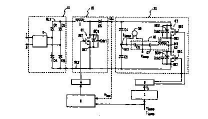
The ballast in~lu~Pc a DC source 10, a boost converter 20, a high
frequency DC-AC square wave inverter 30 and an igniter 40. The el~mPnfc 10-40 ignite the
wog6/20578 2~ ~4~66 PCrm~ss/ollo~
24
lamp and provide a high rl~ue.lcy, s~Jbcl~n~ y cin--cnl~i AC current to the lamp S0. After
lamp igrlitil~n, Control C controls the O~f~ n~ frequency of inverter 30 to avoid arc
inct~bilitiPcl~^ollstir 1~ 50ll~n~ in the HID lamp according to the method ~e5çrihe~1 above.
Control D controls the boost circuit 20 to limit the bus voltage during the lamp ignition
S phase (since the larnp ~lcserlt~ only a small load during this time) to prevent an over-voltage
from being applied to the lamp and to ~l~rntontc of the circuit. Control D also controls the
boost circuit 20 to ,..~;nl~in conct~nt power to the lamp despite ch~nges made by Control C
in the inverter opc-~ t;ng frequency to avoid ~coustic reson~nre Control A operates the boost
converter 20 at the boost frequency dt~.,llined by Control D while Control B opc,~.tcs the
10 inverter 30 at the in~c.~r frequency determined by the Control C.
The DC source 10 inrludes a pair of input terminals 1,2 for receiving a
standard AC power line voltage of 110-120V. A rectifier consisting of diodes Dl-D4
provides a full-wave rectified DC voltage of about 160 V across DC rails RLl, RL2.
The DC source 10 may also include an EMI filter S for incul~-ing the power lines from
lS interference generated by the lamp controller.
The boost converter 20 boosts and controls the DC voltage across rails
RLl, RL2 at a level such that a ~le.~ d power is provided to the HID lamp S0 via the
inverter circuit 30. The boost converter typically boosts the voltage from 160V to about 380
V. The boost converter also provides power factor correction. The converter 20 inrlud~s an
20 inductor Ll having one end conn.~cted to the cathodes of diodes Dl and D2 and its other end
conne~tçd to the anode of diode DS. A switch Ql is conn~ted between DC rails RL2 and
RLl at a junction between the inductor Ll and the diode DS. The switch Ql is a mosfet and
includes a body diode BDl and a parasitic c~r~cif~nce ~ecigrl~t~d Cdsl. The control gate of
switch Ql is co~nPct~d to control A, which provides a periodic voltage signal to control the
25 switching frequency and duty cycle of the switch Ql in a manner to be described in further
detail. The duty cycle and switching frequency control the current flow throw the inductor
Ll so that in conjunction with the c~p~itors C4 and CS of the inverter circuit 30 the voltage
on the DC rails RLl, RL2 across c~r~ C4 and CS is ...~int~;ned coJ-ct~nt at the desired
level. The c~raritors C4 and CS act as an energy storage ck .rnt to provide cor~ct~nt power
30 to the lamp, even when the Line voltage crosses zero.
The inverter circuit 30 is a voltage-fed half-bridge DC-AC inverter with
switches Q2, Q3 series connected across the DC rails RLl, RI2. The switches Q2, Q3 are
mosfets. The source of switch Q2 is connr~ted to rail RLl, the drain of switch Q2 is
conne~ted to the source of switch Q3 and the drain of switch Q3 is conn~ct~d to rail RL2.
wo 96/20578 2 1 8 4 2 6 6 ` PcTnssslollo6
- 25
C~p~ r Cds2 and diode BD2 are the p~r~citir ç~r~rit~nre and the body diode, ~ ely,
of the switch Q2. C~r~ritnr Cds3 and diode BD3 are similarly the p~citir r~ ;lA ~re and
body diode of the mosfet switch Q3. The control gates of switches Q2 and Q3 are CQI~nC~
to control B, which will be descrihed in greater detail. The output of the half-bridge inverter,
S app~ing across points Ml, M2, is a high fi qucncy generally square wave signal as is
f~mili~r to those skilled in the art.
An LCC ntlwclk of c~p~ritors C6, C7 and in~Uct~r L2 are series
conn~-l~d belween a mi-lpoint Ml bel~n the switches Ql and Q2 and a rni~pQint M2bel~n the half-bridge ç~ r;lol~ C4 and C5. The HID lamp 50 is cQnn~t~ in parallel
10 with the c~p~ritor C6. The LCC network provides a wavc~ l ing and current limiting, or
b~ cting, function to provide a s~lbsl~nl;~lly sinusoi~l lamp current to the HID larnp 50
from the inverter output present across the midpoints Ml-M2.
The LCC network also filnctio~c as an igniter to ignite the lamp upon
initial applir~tinn of power to the controller. The LCC network is tuned to a third hz.~ nir
15 of the initial inverter op~ g fi~u~ncy to provide a high starting voltage of about 2500 V
s~le~ted for this specific applir~tion. Starting the lamp at the third harmonic has the
advantage of reduring the initial ignitinn current drawn from the boost converter as COII~
to convention~l first harmonic starting. When the inverter begins opel~ting, an ignition
voltage is caused by reson~nre of the LCC network at the third hd~ onic of the inverter
20 output at the initial olJe~ ~I;ng frequency. After the lamp starts, the i...pe~nçe of the lamp is
much lower than that of the c~p~ritor C7, so the wavecl.~p;ng and current limiting is then
controlled primarily by the LC network of C6 and L2. Thus, the igniter uses the variation in
the lamp impe~nce (from about lM prior to ignition to about 100 at steady state) to shift
the gain of the circuit inçluding the LCC network and lamp from a gain suitable for
25 providing an ignitinn voltage to a lower gain suitable for Op~.atiilg the lamp.
Instead of the LCC network shown, other igniters may used, such as well
known pulse igniters or other l, sonant igniters such as an LC or an LLCC network which
employ ignition at the first or third h~lllonic. Ad~itiol~lly~ in the LCC n~ lwolk shown, an
active frequency shift may be employed by which the inverter op, ~ g frequency is set at
30 an initial frequency (generally higher than the steady state fi~ qu~ncy) for causing the ignition
voltage and then set to a second, different frequency for lamp oper~tion after ignition
Control B controls the ~witching frequency and pulse width of the
swi~clles Q2 and Q3 in a well known manner to provide the subs~ lly square wave AC
inverter voltage across midpoints Ml and M2 at frequencies within a frequency range
wo s6/20s78 2 1 8 4 2 6 6 ~ Pcr/Isss/0ll06
26~ ~;
s~it~ble for ope,~Lu~g the lamps inten~ed to be controlled by the ballast. In this in~t~nre~ the
range is between about 20kHz and 25kHz, which is the pre-s~l~octed O~.AI;ng window, to
avoid strong ~rouctir ræ on~nr~C/arc inct~hilitiPs for the 100 W metal halide lamps A-E
shown in Figure 5c. In particular, Control B is responsive to a frequency control signal from
the Arc Tnct~ility Control C to operate the half-bridge at the frequency de~ign~t~ by the
Control C.
The CilCuiLI~ and operation of Control D and Control A will now be
describe~ in greater detail with lef~cnce to Figures 14 and 15. Control Dinrh~des circuits
for sensing the lamp voltage and lamp current at locations V~,p and ILamP shown in Figure
13. The lamp voltage is sensed at voltage sensing circuit 60 as shown in Fig. 14 which
inrludes a voltage divider inrlurling resistors R11 and R12 and the r~r~citor Cll. The
function of the c~ r;lor Cll is to isolate the DC col"ponent between the sensed lamp
voltage at point VLamP and ground. The diode Dll has its anode conn~rted between the
resistors R11 and R12 and its cathode connertt~d to one side of the resistor R13. The other
side of the resistor R13is co~n~rt~ to ground. The c~r~ritor C12 and the zener diode D12
are cor-nPrtPd in parallel with the resistor R13. The cathode of the zener diode D12is
conn~rted to the cathode of the diode D11. The diodes D11 and D12 form a half-wave
rectifier to provide a DC voltage VL at the resistor R13 1~1~SenlahVe of the sensed lamp
voltage Vlamp-
The lamp current is sensed by current sensing circuit 70 which inrlu~es
current transformer T. ConnPctçd in parallel with transformer T are resistor R14,c~r~ritor
C13 and resistor R15. The anode of diode D13is connected to one side of the current
transformer T while its cathode is connP~ted to resistor R15. The output of current sensing
circuit 70is a DC voltage Vi which is linearly plopol~ional to the larnp current ILal~P-
The Control D further inrludes a multiplier 61 which mnltirli~ the signal
VL rep~s~ .1;ng the lamp voltage with the signal Vi le~ sent;.lg the lamp current to obtain
signal Vp l~ s~..t;ng the lamp power. The diode D14 and the resistor R19 are series
connected belween the output of the multirli~r 61 and the inverting input of the error
amplifier 65. The non-inverting input of the error amplifier 65 receives a reference signal
Vpref indicative of the desired op~ting power for the HID larnp 50 or Vref indicative of the
upper limit for the bus voltage. Resistor R20isconnPcted between a junction between the
resistor R19 and the inverting input of the error ~mplifiPr 65, and ground. Resistor R21is
conn-~led bt~ n the inverting input and the output of the error ~mplifi-or65. The
co,..p~.lLor 67 receives the output of the error ~mplifi~r at its non-inverting input and a
wo 96/20578 2 1 8 4 2 66 ~ B95/01106
27
w~th waveform output of the oscillAtrJr 63 at its inverting input.
The c~ pA~ or 71 co~ .~es the signal Vj received at its inverting input
with a signal Vn received at its positive input. The diode D15 has its cathode cQnn-~d to
the output of the co,~.p~Alor 71 and its anode connee~ed to the anode of diode D6. The
5 cathode of diode D16 is conn~tçd to one side of the resistor R18, the other side of which is
conn~rt~d to the inverting input of the error ~mplifiPr 65. A voltage divider inrlu~in~ the
resistors R16, R17, is connr~l~ between the anodes of diodes D15 and D16. One end of the
resistor R16 is cQnn~ d to the DC rail, or bus, RL1 at the lor~tion illllCt~t~d in Figure 13.
A voltage V3 ~ g the bus voltage is therefore present at the midpoint between the
10 resistors R16, R17.
During i~ni~on of the lamp 50, the Control Circuit D ope..ltes in a bus
voltage control mode. During this time, the larnp is not yet on and has a high impe~l~nre As
a result, the load on the boost converter 20 is light and the voltage on the DC rails RL1,
RL2 will signifirrlntly increase without other measures being taken. After ignitirJn the
15 i".~i~nre of the larnp decleases, and the current drawn by the larnp increases, until the
lamp reaches steady state. Limits on the bus voltage are needed during ignitior~ and steady
state to prevent catastrophic op~Al;ng con~lition~ inclu~ling near lamp end-of-life. Control D
senses the bus voltage VbUs and feeds it to the control A which adjusts the pulse width of the
boost switch Q1 to keep the bus voltage at a prede~ ined voltage during the ignition phase.
20 Since the lamp has a high i...pell~nre, the current through the larnp has a small value which
is sensed by the current transformer T and then rectified through the half-wave rec~ifier D13.
The DC voltage Vi, which is linearly propolLional to the lamp current, is almost zero since
there is little lamp current during ignition. In addition, the output of the mllltipliPr 61 is
smaller than the fefelence voltage Vref which results in blocking the diode D14, making the
25 power control loop inactive during this period. The voltage Vj is col-lpared with the voltage
Vrj through the co---p~A~or 71. When Vi is less than Vrj~ as is the case during ignitir,rl, the
output of colllpdldtor 71 is a high voltage V2 As a consequence, diode D15 is reversed
biased and the bus voltage control loop is active. Thus, D16 is turned on or off depen~ing on
the value of the bus voltage.
When the voltage control loop circuit starts up at larnp igrlition, when the
lamp p~sents a very small load, the bus voltage increases rapidly and is sensed through the
voltage divider of resistors R16 and R17. While the sensed voltage V3 iS less than the
reference voltage Vref at start up, the diode Dl6 lt;lllahls off. The output of the error
~mplifi~r, in the initial circuit con~ition prior to conduction of diode D16, is given by
w096120578 2 1 ~426 6 : PCI/IssS/01106
Vo = (l+R2~)Vf
The voltage VO is co",p~d with the saw tooth waveforrn generated by the oscill~tor 63 to
get the pulse width control for the boost switch Ql, thereby controlling the energy stored in
the electrolytic c~ c;~ots C4, C5 (Fig. 13). By design, the duty ratio of the boost stage has
a m~Yimllm value set at about 0.48. Once the sensed voltage V3 reaches the reference Vref,
S the diode D16 starts contlucting. The sensed bus voltage is fed to the inverting terminal of
the error ~mplifiPr 65 through the resistor R8. The output voltage VO of the error ~mrlifiPr
65 is given by
V = ~R21 + R21~ Vr~f _ R2 (V3 - VD)
~20 18 18
where VD is the forward voltage drop across the diode D16. The voltage VO and the output
voltage of osc~ t~.r 63 are fed into the co~ t-,r 67 to obtain the pulse width control of
10 the boost switch Q1. Figure 15 ilh.c~ tos the voltage VO, the sawtooth waveform from the
osc~ tor 63, and the output waveform of the co~ tn~r 67, which is the gate source
voltage Vgsl controlling the boost switch Ql. The smaller the voltage VO is, the smaller the
pulse width will be of the control signal Vgsl controlling the switch Q1..Cons~uenlly, the
pulse width will decrease when the sensed bus voltage V3 increases. Based on the operation
15 of the boost converter, the bus voltage will be reduced and kept within a prefell~d range of
450V for eY~mple
After ignitinn of the HID lamp 50, the control circuit D switches to a
power control mode to control the power to the lamp. Without further measures, the power
applied to the larnp will change when the Control C changes the op~.~ting frequency of the
20 lamp to control arc inst~bility because the gain of the resonal t LCC network or any other
ignition topology, and therefore the power delivered to the lamp, varies with the inverter
output frequency. ~en~rally cr~king, in tne power control mode, the lamp current and lamp
voltage are sensed and mllltiplied to obtain the total power in the lamp. The lamp power is
cG",paled with a reference power signal with the objective of ch~ngjn~ the duty ratio of the
25 boost switch Ql to regulate the bus voltage across RL1, RL2, which results in adjuc~--en~ of
the power delivered to the lamp.
Once the lamp 50 has ignited, the voltage signal Vi is larger than the
218~266
Wo 96/20578 PcrlIBsslollo6
29
,~f~, ce voltage Vri. The co...p~ o~ 71 outputs a low voltage V2 which leads to the
co~-lv~ l;on of the diode D15. As a result, the sensed bus voltage Vbw is cl~mre~ ren~Pring
the bus voltage control loop inactive, and the power control loop be~o~ s active. The sensed
lamp voltage VL and lamp current Vi signals are fed to the mllltirliPr 61 to obtain a power
S signal Vp of the lamps, which will be col,lparcd with the rerc.~ ncc power Vpref to control the
pulse width of the boost switch. If the sv~i~cl~ing rl~uency of the half-bridge inverter
rl~nges the power delivered to the lamp will increase or decrease since the voltage gain
value for the igniter is different for different inverter operating frequenciPs
A decr~ in the power transferred to the lamp will be ~cs~lmP~ as an
10 e~ le to illllc~r~te the operation of the power control loop. The sensed lamp power Vp
from the mllltipliPr 61 is supplied to the inverting terminal of the error ~mplifiPr 65 through
the resistor Rl9 and the diode D14 and then CGIllpal~,d with the reference power Vpref. In the
power control mode, the output voltage VO of the error ~mpiifiPr 65 is given by
V = (l+ RZI + R2,) V f - (V1-VD)
R20 ~9
Th~ l~fole, VO will increase when the sensed power Vp decreases. When the sensed lamp
15 power Vp dec.eascs, V0 increases and the pulse width of Vgsl increases. When the pulse
width increases, the boost switch remains on for a longer period of time within each cycle,
thereby increasing the bus voltage across rails RL1, RL2. As a result of the increase in the
bus voltage Vbus, the power delivered to the lamp increases. This negative fe~db~ keeps
the lamp power the same as the reference power set by the signal Vpref. On the other hand,
if the lamp power increases due to a change in the half-bridge switching frequency by the
Control C, the sensed power Vp becGI~les larger, leading to a decrease in the pulse width of
the driving signal V,~s1 for the boost switch Q1. The boost converter will then be lower the
bus voltage on rails RL1, RL2 until the sensed power equals the lcr~.~.,ce power value Vrep
Certain HID lamps have a tendency to draw more power near the end of life than their rated
wattage, which can lead to Ca~L,~hic lamp failure if this higher power is supplied by the
ballast. Since the power control mode limits the power supplied to the lamp, it serves to
prevent catastrophic failure. Rather, the lamp will simply fail to operate when the power
corresponding to the signal Vpref is inCuffi( iPnt to meet the higher power required by the
lamp at its end-of-life.
From the above analysis, it can be seen that control D has two control
WO 96t20578 2 ~ ~4 2 66 PCI/IB95tO1106
. .
modes, which are the voltage and power control modes. One objective of the voltage control
mode is to clarnp the bus voltage during lamp ignitinn and prior to steady state ope~tinn
The bus voltage control can also be used to prevent cataaL ol)hic lamp end of life, where the
lendenc~l of the ballast is to provide excessive power to the lamp due to the i.,.~~
S variation with lamp life. The objective of the power control mode is to deliver a cQnct~nt
power to the lamp even with changPs in the switching frequency and in the line voltage.
Figure 16 is a circuit ~iagram for the controls A and D of Fig. 13.
Co.~ronPI~tc the sarne as those diccuccpd in Figure 14 bear the same lefclence nllmP~lc The
mnltirliPr 61 of Fig. 14 is embodied in a 14 pin IC (model AD534 available from Analog
10 Device Corp.). VL is input at pin 1 and Vi is input at pin 6. The oScill~tor 63, error
amplifiPr 65 and the co.~.p~..,tol 67 are embodied in a 16 pin high speed PWM controller 80
(model UC 3825 available from Unitrode Corp.). The UC 3825 is optimized for highfrequency switched mode power supplies and directly controls the switching of the mosfet
Ql. The source SQ1 of switch Q1 is connPrted to pins 9, 10 and 12 and to ground. The
15 gate GQ1 of switch Q1 is connp l~ d to pin 14 via the resistor R22. In Figures 16 and 18, the
pin connP.-I;onc not srecifi~lly descrihed herein are shown merely for the sake of
complet~PnPcc and are not nPo~Pcc~ry for the underst~n~ing of the invention. Such cQnnP~tinnc
are sperifiP~ by the IC m~mlfa- tnrer.
As shown in Figure 17, the Control C for Arc Instability Control int~lu~es
20 two A/D converters 90, 95 for converting the sensed lamp voltage VL and la np current Vi to
a ~ ecLi-/e digital signal. The signals VL and Vi are tapped from the circuits 60, 70 of
Figure 14. The control C further in~ des a miclu~ocessor 100 which implPment~ the
program of Figure 9 in soflw~c to control the operating frequency of the half-bridge inverter
30. The microprocessor 100 receives the sensed lamp voltage and lamp current from the dual
25 A/D converters and outputs a digital signal which is converted to an analog signal f5 by the
A/D converter 105. The signal f5 ~ se,-ts the inct~n~nPous frequency output by the
software program in conducting any of the modes of operation according to the method
previously d~Pscrihed
By implpmpnting the program of Figure 9 in sofLw~c in the
30 microp~ocessor 100, the Control C in~]udes means for carrying out each of the method steps
hereinbefore described with respect to detection of the frequencies at which a~ouctic
reson~ncP/arc instability occurs and for ch~nging the frequency of the inverter to a new
center op~ ~I;ng frequency. Thus, for example, with respect to the frequency sweep of
Figure 2, the Control C includes means for varying the opclating rl~u~ ncy over a plurality
WO 96/20578 2 1 8 4 2 6 6 PCT/IB9S/01106
31
of distinct ope ~ 'e frequenrif s for mf~cnring a plurality of c~mp~- - of an el~trir~l
p~mftPr of the lamp at each of the plurality of distinct op~ ~I;ng freq~lfnries~ and means
for c~1rul~tine, at each of said plurality of opc~dting freq~Pnrif c, the standard deviation of
the ~mrlPs taken at each frequency, and means for ev~ln~tine, for example det,octing the
S cm~llPst s~ndaf~ deviation, to select a new center frequency.
The self~tinn of cG.~pQnf ~l~ for the control C is based on the desired
precision and ~mpling speeds nf~cc~ for effectively imple...c~l;ng the pn~,ldlll of Figure
9 and depfnr~s on lamp type, physical and chfmic~l plu~.lies, lamp power and ~limfn~ nc
In one imple,..f ~ ;on, the ...;n;..".... number of ~mrles for lamp current and voltage to
10 obtain one standard deviation me~ulc",ent at one frequency was selfxte~d as 20. S~mrlPs
were taken at 100 individual frequencies in each frequency sweep, so a total of 100 times 20,
or 2000 ~mrles are taken in each frequency sweep. The sampling speed should be slow
enough to allow the arc to react but fast enough to prevent large arc movc."en~s. A suitable
range for ~mpline speed is between 50 msec and 100 msec for 100 W metal halide lamps.
The rninimnm precision of the AtD and D/A converters 90,95,105 and of miclu~
100 was sPk~led to be 0.005 which is ~ticfiPd by 8-bit devices (8-bits=1/256=0.004). In
the implemPnt~tirJn shown in Figures 13, 14 the A/D converters are an 8-bit, high speed
model ADC 0820 available from Linear Technologies. The D/A converter was also 8-bit;
model NE 5018 available from SienPtirs The micrûl)locesso~ was an 16Mhz, 8-bit
p~<,cessor, model No. 87C550 with 4K of EPROM available from Philips Semir~nductors.
The software program of Figure 9 was programmed in the Assembler language. Thesedevices provide a ~mpline rate of 10 kHz to 20 kHz for the lamp current and voltage with a
c~mpling speed of between 50 msec and 100 msec., which was found to be snffiriPnt for
effectively det~P~ting and avoiding ~rouctir reSol-~nre in 100W metal halide lamps.
Control B use well-known techniques for driving the half-bridge inverter
with the exception that it drives the half-bridge inverter at a fi~uency in~ir~t~d by the
control C rather than at a co~.sl~i-t frequency as is usually done. A circuit impl~Pm~Pntine
Control B is illustrated in Figure 18. The circuit includ~Ps IC's 110 and 120. IC 110 is a 16
pin, high speed controller (model UC3825 available from Unitrode) which serves to receive
30 the frequency design~ting output signal fs from the Control C and provide control signals for
input to the IC 120. The IC 120 is 14 pin, high voltage, high speed MOS gate driver (model
IR 2110 available from Tnt~Prn~tion~l Rectifier). The IR 2110 has both high and low side
~fe,ellce output ch~nnPl~ and is esperi~lly useful for half-bridge ap~lir~tion~ since it has
intern~lly set dead-time control. The IC 120 provides the gate\source drive signals to the
wo 96120s78 2 1 8 ~ 2 6 6 PcrlIssslollo6
32
mosfet s~vitches Q2, Q3. The output signal of the Control C is input at pins S and 6, which
serves to contrd the duty cycle v~ri~tinn
The output of IC 110 is taken from pins 11 and 14 and are input at pins
12 and 10, ~ ely, of the IR 2110 (IC 120). The gate GQ2 of switch Q2 (Fig. 3B)is
S connprt~ to pin 1 via the resistor R31. The diode D31 is c4nn~ d in parallel with the
resistor R31 with its c~thode connP~.t~d to pin 1 and serves to prevent a negative bias at this
pin. Simil~rly, the gate GQ3 of switch Q3 is conn~p~ted to pin 7 via the parallel ~ gf.l.~n
of the resistor R32 and diode D32, which serve the same function as the resistorldiode
nclv~ol~ con~ d to pin 1. The source SQ2 of switch Q2 and the source SQ3 of switch Q3
10 are cof nP~ted to pins 2 and 5, lc~e~ ely.
The mi~;lop~ocessor may be lJlu~ ed to include different c~.,.bi~ nc
of the steps herein decrribe~ and/or use one described option instead of another. For
example, the controller may select an opc~dling r~ u~,.,cy which occurs at a broad .~.;l-;...~..
rather than at a nallu~ ~, but smaller, miniml-m or implemrnt the Open loop routine at
15 different points during run-up and steady state, as ~icrucc~Pd for eY~mrle~ with respect to
Figures 5(a) - S(c). rul~ ,lore, the controller\ballast could be implrmrntpd in a mod~ r
system for n with the controller inrlurling one or more parts each pc.rulll,ing sPl~t~
funrtit rlc and outputting signals to other modlllPc In this contpyt~ for example, the m~~ r
system could include a ballast with a controller d~PcignP~ to coopc .~ with a series of control
20 devices, each of which pc.ro~ll,s a sel~ted combination of the fimrtionc described herein.
From the above description, it can be seen that Applicants have
discovered certain steps which are universally applicable to gas discharge lamps for det~ting
and avoiding arc instabilities and which are particularly useful for det~ting/avoiding arc
instabilities due to ~Goustir, rec~ n~nre. These steps may be imple..~ented in many dirr.,.el~t
25 ballast topologies, inr~ ing single stage (such as ~isclosed in U.S. ~pplir~tion SeAal No.
08/197,530, filed February 10, 1994) and two stage b~ Ctc, and as already diccusc~d~ may
employ different igniters. The control is applicable for all (or a great) frequency range(s),
basically from O Hz to several MHz and with no perceived upper limit. T imit~tionC are
related to the speed of ~mpling and proceccing (which will be ovelcollle by faster
30 pf~cessol~) and most hll~l~lLly by ballast (hardware) construction.
With a gain of the inverter highly conct~nt across a broad rl~uency
range, will allow a large frequency sweep range to be implP....~nl*~ and will &Pnr~lly
obviate the need for the described pre-selection of a broad rl~uen~ window by the
~ecignPr. This will allow an even greater universality of the control; for ~ , p~"..;~ g
wo s6nos78 218 4 2 6 6 pcrlIBsslollo6
33
a universal controller module to be plugged into ballasts optimized for different wattage
ranges.
The method makes the ballast quite incpncitive to lamp ~imPncinn~l
v~ri~tinnc (in productinn lines), chPmi~l modifications along lamp life, and changes in lamp
5 ch~t~Prictirs during its life. The method allows use of high frequency electronic ballasts to
run HID lamps and avoids lamp destruction and catastrophic end of life. This control makes
the ballast quite immlmç to the lamp, since it is smart, universal, general and flPYihlP