Language selection

Search

Patent 2185026 Summary

Third-party information liability

Some of the information on this Web page has been provided by external sources. The Government of Canada is not responsible for the accuracy, reliability or currency of the information supplied by external sources. Users wishing to rely upon this information should consult directly with the source of the information. Content provided by external sources is not subject to official languages, privacy and accessibility requirements.

Claims and Abstract availability

Any discrepancies in the text and image of the Claims and Abstract are due to differing posting times. Text of the Claims and Abstract are posted:

  • At the time the application is open to public inspection;
  • At the time of issue of the patent (grant).
(12) Patent Application: (11) CA 2185026
(54) English Title: METHOD AND APPARATUS FOR REDUCING QUANTIZATION NOISE
(54) French Title: PROCEDE ET APPAREIL DESTINE A REDUIRE LE BRUIT DE QUANTIFICATION
Status: Deemed Abandoned and Beyond the Period of Reinstatement - Pending Response to Notice of Disregarded Communication
Bibliographic Data
(51) International Patent Classification (IPC):
  • H03M 01/08 (2006.01)
  • H03H 17/02 (2006.01)
  • H03M 01/66 (2006.01)
  • H03M 07/36 (2006.01)
  • H04B 01/26 (2006.01)
  • H04B 14/04 (2006.01)
  • H04L 01/06 (2006.01)
  • H04L 01/22 (2006.01)
(72) Inventors :
  • LUZ, YUDA YEHUDA (United States of America)
  • LONG, JAMES FRANK (United States of America)
(73) Owners :
  • MOTOROLA, INC.
(71) Applicants :
  • MOTOROLA, INC. (United States of America)
(74) Agent: GOWLING WLG (CANADA) LLP
(74) Associate agent:
(45) Issued:
(86) PCT Filing Date: 1995-12-28
(87) Open to Public Inspection: 1996-08-22
Examination requested: 1996-09-06
Availability of licence: N/A
Dedicated to the Public: N/A
(25) Language of filing: English

Patent Cooperation Treaty (PCT): Yes
(86) PCT Filing Number: PCT/US1995/017018
(87) International Publication Number: US1995017018
(85) National Entry: 1996-09-06

(30) Application Priority Data:
Application No. Country/Territory Date
08/389,474 (United States of America) 1995-02-14

Abstracts

English Abstract


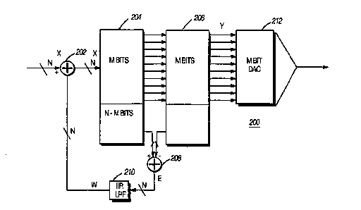
In a quantization noise reduction circuit (200), a feedback signal (W) is added to an input signal (X) to the quantization circuit
to reduce quantization noise. The feedback signal is generated as a filtered difference between a sample of an N bit signal (X') and a
time coincident sample of an M bit quantized signal, where M < N. The feedback signal is subtracted from the input signal (X) prior to
quantization thereby introducing out of band noise into the input signal for reducing in band noise in the quantized signal (Y).


French Abstract

Dans un circuit de réduction du bruit de quantification (200), un signal de rétroaction (W) est ajouté à un signal d'entrée (X) dans le circuit de quantification afin de réduire le bruit de quantification. Le signal de rétroaction est généré en tant que différence de filtrage entre l'échantillon d'un signal (X') à N bits et un échantillon à coïncidence temporelle d'un signal quantifié à M bits où M < N. Le signal de rétroaction est déduit du signal d'entrée (X) avant la quantification, ce qui permet d'introduire du bruit hors bande dans le signal d'entrée afin de réduire le bruit de bande dans le signal quantifié (Y).

Claims

Note: Claims are shown in the official language in which they were submitted.


-6-
CLAIMS
1. An apparatus for reducing quantization noise comprising:
a first adder having a first input coupled to receive a N bit input
signal;
a N bit latch having an input coupled to receive an output of the
first adder;
a M bit hard quantizer having an input coupled to receive an
output of the N bit latch, where M < N, and an M bit output;
a second adder having a first input coupled to receive a N bit
sample from the N bit latch and a second input coupled to receive a N
bit sample from the M bit hard quantizer where the N bit sample from
the M bit hard quantizer comprises M bits of the N bit sample and at
least one N - M zero bit;
a filter having an input coupled to receive an output of the
second adder and an output coupled a second input of the first adder.
2. The apparatus of claim 1 wherein the first adder is operable to
take a difference between the first input and the second input.
3. The apparatus of claim 1 wherein the second adder is
operable to take a difference between the first input and the second
input.
4. The apparatus of claim 1 wherein the filter is a low pass filter.
5. The apparatus of claim 1 wherein the filter has a cut-off
frequency substantially below a usable bandwidth of the N bit input
signal.
6. The apparatus of claim 1 wherein the filter has a gain greater
than unity.

-7-
7. The apparatus of claim 1 wherein the N bit sample from the M
bit hard quantizer comprises M most significant bits of the N bit
sample from the N bit latch and at least one N - M zero bit.
8. The apparatus of claim 1 wherein the N bit sample from the M
bit hard quantizer comprises M most significant bits corresponding to
M most signficant bits of the N bit sample from the N bit latch and N -
M zero bits.
9. A method of reducing quantization noise:
taking a difference between a N bit sample of a N bit input
signal and a N bit quantized sample comprising bits of the N bit
sample, where M < N, and N - M zero bits;
filtering the difference to form a filtered difference; and
subtracting the filtered difference from the N bit input signal.
10. The method of reducing quantization noise as in claim 9
wherein the step of taking a difference comprises taking a difference
between a N bit sample of a N bit input signal and a N bit quantized
sample comprising M most significant bits of the N bit input signal and
N - M zero bits.

Description

Note: Descriptions are shown in the official language in which they were submitted.


WO 96125809 2 1 8 5 a 2 6 PCTNS95/171118
-1 -
METHOD AND APPARATUS FOR REDUCING
QUANTIZATION NOISE
Field of the l~l~rc.llio
The present invention relates generally to digital signal
pruues:~ir~!J and more particularly to a method and apparatus for
reducing quantization noise in digital signal ~,~ces~i"g 1" ' ~s.
Background of the l"~_l,lion
Digital signal ~,ucessi"u, is evolving as the preferred
;III~JIC Illt:llldliul~ in many signal ,~uces~ g _p,~ ~b. The advent
of improved, higher speed and lower cost digital signal pruuea
15 (DSPs) and other digital circuit elements coupled with increased
flexibiiity and accuracy of digital circuits is driving a move to
converting a number of signal ~,,u~e:,aillg ap; ~5 from the
analog forum to the digital fonum. Digital signal p,u~aasi,,g while
offering the above ",~:"liol,ed advantages and other advantages,
20 does not come without some dl uL- For example some
1r ~s, particularly in the field of radio frequency (RF)
communications are inherently analog. Signal p,~ces:,i"g for RF
often require converting an analog signal for example
an RF or i"l~""adid~ frequency (IF) signal to a digital signal and
25 likewise converting digital signals to analog signals.
In many digital ,UI u~ ~S~il l9 1 ~, 15, including those
accu",u~ ed in a wideband digital transceiver, the precision of a
signal must be converted from a high level of precision to a lower
level of precision. For example a signal Itu~s~lad as 32 bits of
30 illlUlllldliUI1 may have to be reduced to a signal l~ult,s~ d as 16 bits
of illfvlll .I. This is due to the limited ~rr' - of certain digital
plu~s~ lg elements such as, for example digital-to-analog
converters (DACs~. In making such a conversion however, there is a
loss of i"'~ Illdli~l1. One will d,~ulc:~dlt~ in the above example that 32
3.~ bits can represent more ill~UlllldliUII than 16 bits at a given data rate.
The result of this loss of ill~Ulllldliol, is quantization noise.

W096/2S809 2 1 85026 PCT/US95/17018 ~
-2 -
Referring to FIG. 1, a typical example is shown to illustrate the
effects of quantization noise. In the .,, 'i , illustrated, a 16 bit
digital signal X of given frequency is to be converted to an analog
signal by DAC 10. However, DAC 10 is only a 12 bit device.
5 Therefore, the signal X must be first converted to a 12 bit signal. A
typical approach is to use a hard quantizer 12 which truncates the
least significant bits (LSBs), in this case the 4 LSBs, of signal X to
create a 12 bit signal Y. The noise relative to the carrier signal in
decibels (dBc) of this I, ~' n is given as:0
noise (dBc) = 20 log 2-n
where n is the number of bits of the DAC. Thus, the noise levei is (-
72) dBc for the 12 bit DAC and would be, for example, (-78) dBc for a
15 13 bit DAC, etc. Often the noise is distributed overthe entire Nyquist
bdll '\.;d~ll and the noise power per Hertz is negligible. However,
frequently the noise appears at discreet frequencies, like second and
third har,,lullics of the signal, which pose significant problems.
To overcome the problem of noise dwelling at particular
20 frequencies, it has been proposed to introduce psue~uldndu,,, noise
to the signal, often referred to as dithering. A number of dithering
techniques are taught in U.S. Patents Nos. 4,901,265, 4,951,237,
5,073,869, 5,228,054 and 5,291,428. A major disadvantage of
dUhering is the requirement of having to provide pseu~uldl-d~", noise
25 generator circuitry which is often complex making the
illl,Ul~ llLdliu17 intensive and costly.
Therefore, a need exists for a method and apparatus for
reducing quantization noise without siy" " I~ly increasing the cost
and c~",,ul~xi~y of the digltal signal p,uces:,i"g circuit.
Brief D~ s ;~,liol, of the Drawings
FIG. 1 is a block diagram IC:,UI~5~" ~ of a prior art 16 bit to
2 bit quantization circuit;

2 1 85026 i
WO 96/25809 PCT/US95/17018
-3 -
FIG. 2 is a block diagram r~ se"ldtiu" of a quantization
circuit in acco,da"ce with a preferred ~",bo~i",~"l of the present
invention;
FIG. 3 is a transfer function rt:ult:s~l lldli~l~ of a filter for use in
5 the quantization circuit shown in FIG. 2;
FIG. 4 is graph spectrally illustrating quantization noise based
upon truncation without the present invention; and
FIG. 5 is graph spectrally illustrating the ~ v~ al~ce of the
quantization circuit of FIG. 2.
Detailed De i~,lion of the P,~ F~ d E~ 3 ,l
According to the present invention, a feedback signal is
provided to the input of a quantization circuit to reduce quantization
15 noise. The feedback signal is generated as a filtered difference
between a sample of the N bit signal and a time c~i"ciclt~"I sample of
a M bit quantized signal where M < N. The feedback signal is
subtracted from the input signal prior to quantization thereby
introducing out of band noise into the input signal for reducing in
20 band noise in the quantized signal.
With reference to FIG. 2, a N bit to M bit where M < N,
quantization circuit 200 in dccor~dl~ce with the present invention is
shown. A N bit signal X is coupled to a summer 202 where a N bit
feedback signal W is subtracted. The resulting signal X' is then
25 sampled in a N bit latch 204 and ~ol~colllitdl '~y quantized in a M bit
hard quantizer 206. Hard quantizer truncates the N - M LSBs of
signal X' effectively setting the M - N LSBs to a value of zero. A N bit
enror signal E, is generated in summer 208 as the difference between
the M most ~iyl li~i~;dliUI, bits (MSBs) of the N bit sample of X' ~=
30 contained in latch 204 and the M bit quantized sample contained in
hard quantizer 206. The LSBs of the N bit sample of X' pass
Ull~ l,anged. Error signal E is filtered through filter 210 creating N bit
feedback signal W. It should be dpplt:~ idlt:d, however, that any M bits
of signal X' may retained in hard quantizer 206 d~u~,,.l;,,g on the
35 particular l~F i~n.

W096/25~09 ~ J.,,JIllVi~
-4-
Further shown in FIG. 2 is a 12 bit DAC 212 for converting hard
quantizer output signal Y to an analog signal. It should be
~"~ ood, however, that quantization circuit 200 of the present
invention is useful in any digital signal lu,uces:,i"g , ,~' ,
5 requiring a conversion from a high precision ill~u,,,,aliol) signal to a
lower precision il~fulll~dliull signal where it is critical to avoid
introduction of quantization noise.
Filter 210 is chosen to pass only c~""uu"~"l~ of error signal E
which are out of band with respect to input signal X. In the preferred
10 t""Lo~i",~"l, filter 210 is a low pass filter which sUL::~ld,~';l'~/
maintains the noise cu,,,,uu,,~,,t~ introduced into signal X' by
feedback signal W at low frequencies and away from the band of
interest. This is illustrated in FlGs. 4 and 5. As can seen in the FIG. 4,
without the present invention, spurious noise Cul",u~ ";~, illustrated
at fs. having signicant energy are present around the signal of
interest illustrate at fx As can be seen in FIG. 5, while there is a
substantial amount of energy below a frequency ffco, the cut off
frequency of filter 210, there is only a low level of noise which is
sul,:,ld"ti~lly evenly distributed about the signal of interest at
frequency fX In testing the present invention, a noise floor of (-93)
dBc was observed about fX as compare to (-72) dBc as may be
typically expected from a 12 bit quantizer without the present
invention. These data were generated ,~f~.~",;i"g the analog signal
output of DAC 212.
Another feature of the quantization circuit 200 is that when
signal X is not present, or is suL:,ld, .ti..lly zero, there is no noise
output. With prior art dithering techniques, psuedu,dlldu", noise is
continuously input to the quantization circuit. When no input signal is
present, the output signal of the quantization circuit is the
30 pseudorandum noise. In the present invention, when input signal X is
absent or su~:,ldl ,ti~lly zero, the difference taken between the N bit
sample of X' and the M bit quantized sample is suLa~d"~i. l'y zero.
Hence, the output of quantization circuit 200 is zero when no input
signal is present.

WO 96t25809 2 1 8 5 0 2 6 PCT/IIS95117018
-5-
As described with respect to a preferred implt~ ldlioll of
quantization circuit 200, error signal E is a 16 bit signal. However,
since it is the N - M LSBs which primarily contribute to error signal E,
a N - M bit signal could be 5llh5titllt~i In such an illl,ulc~ llldliun, the
sign illfU~ dliol~ of error signal E will be lost. Hence, it may be more
desirable to illl,ul~ lll a (N - M) + 1 bit error signal which retains the
sign bit from signal X'. Such an illl,UItlll~llldlio,~ simplifies the data
path for error signal E as well as reduces the size of filter 210.
With reference to FIG. 3, a transfer function for a preferred
0 il 11~ l lel lldliOIl of filter 210 is shown. As can be seen in FIG. 3, filter
210 is a 3 real pole filter which can be illl~Jl~lll~lllt~d using three full
adders 302, 304 and 306 and one delay element 308. In the
preferred ~",l,odi",e"l of the present invention, the poles of filter 210
are selected to be at 15/16 which allows for the simplified
illl,UIellll:~llldliUl~ shown in FIG. 3. As can be seen, this illlpl~ llldliu
advantageously cl;.llilldl~s the need for multipliers which allows a
simplified illl,Ul~ llldliol~ of filter210 in an ~,, " 'i~., specific
integrated circuit (ASIC). Filter 210 further includes an overall gain
factor, in the preferred ~",~io.li",t:"l ap,ulu~illldl~ly 100 dB. Gain is
provided at each stage of filter 210 which enhances the level of
feedback signal W with respect to input signal X and hence the noise
generating effect of feedback signal W on input signal X.
As will be d,U,JI~ ' from the foregoing, the quantization
circuit 200 of the present invention provides for a greatly simplified
illl~ul~ llldliul~particularlywithrespecttoASICi"l~ llldlioll The
c~;~ll;lldlio~ of the pseudurdi,d~", noise generator previously required
for dithering techniques and advantageous selection of filter design
minimize required gates in the ASIC. These and many other
advantages and uses of the present invention will be a,u,u,~cidled by
3û those of ordinary skill in the art from the foregoing des.;,i~,~iu17 and the
following claims.
We claim:~

Representative Drawing
A single figure which represents the drawing illustrating the invention.
Administrative Status

2024-08-01:As part of the Next Generation Patents (NGP) transition, the Canadian Patents Database (CPD) now contains a more detailed Event History, which replicates the Event Log of our new back-office solution.

Please note that "Inactive:" events refers to events no longer in use in our new back-office solution.

For a clearer understanding of the status of the application/patent presented on this page, the site Disclaimer , as well as the definitions for Patent , Event History , Maintenance Fee  and Payment History  should be consulted.

Event History

Description Date
Inactive: IPC from PCS 2022-09-10
Inactive: First IPC from PCS 2022-09-10
Inactive: IPC from PCS 2022-09-10
Inactive: IPC expired 2009-01-01
Inactive: IPC from MCD 2006-03-12
Application Not Reinstated by Deadline 1999-12-29
Time Limit for Reversal Expired 1999-12-29
Inactive: Abandoned - No reply to s.30(2) Rules requisition 1999-02-24
Deemed Abandoned - Failure to Respond to Maintenance Fee Notice 1998-12-29
Inactive: S.30(2) Rules - Examiner requisition 1998-11-24
Inactive: Status info is complete as of Log entry date 1998-07-23
Inactive: Application prosecuted on TS as of Log entry date 1998-07-23
All Requirements for Examination Determined Compliant 1996-09-06
Request for Examination Requirements Determined Compliant 1996-09-06
Application Published (Open to Public Inspection) 1996-08-22

Abandonment History

Abandonment Date Reason Reinstatement Date
1998-12-29

Maintenance Fee

The last payment was received on 1997-09-19

Note : If the full payment has not been received on or before the date indicated, a further fee may be required which may be one of the following

  • the reinstatement fee;
  • the late payment fee; or
  • additional fee to reverse deemed expiry.

Patent fees are adjusted on the 1st of January every year. The amounts above are the current amounts if received by December 31 of the current year.
Please refer to the CIPO Patent Fees web page to see all current fee amounts.

Fee History

Fee Type Anniversary Year Due Date Paid Date
Request for examination - standard 1996-09-06
MF (application, 2nd anniv.) - standard 02 1997-12-29 1997-09-19
Owners on Record

Note: Records showing the ownership history in alphabetical order.

Current Owners on Record
MOTOROLA, INC.
Past Owners on Record
JAMES FRANK LONG
YUDA YEHUDA LUZ
Past Owners that do not appear in the "Owners on Record" listing will appear in other documentation within the application.
Documents

To view selected files, please enter reCAPTCHA code :


To view images, click a link in the Document Description column. To download the documents, select one or more checkboxes in the first column and then click the "Download Selected in PDF format (Zip Archive)" or the "Download Selected as Single PDF" button.

List of published and non-published patent-specific documents on the CPD .

If you have any difficulty accessing content, you can call the Client Service Centre at 1-866-997-1936 or send them an e-mail at CIPO Client Service Centre.


Document
Description 
Date
(yyyy-mm-dd) 
Number of pages   Size of Image (KB) 
Description 1996-08-21 5 235
Abstract 1996-08-21 1 40
Claims 1996-08-21 2 58
Drawings 1996-08-21 3 48
Representative drawing 1997-10-20 1 6
Reminder of maintenance fee due 1997-08-30 1 111
Courtesy - Abandonment Letter (Maintenance Fee) 1999-01-25 1 184
Courtesy - Abandonment Letter (R30(2)) 1999-04-20 1 172
PCT 1996-09-05 1 48