Note: Descriptions are shown in the official language in which they were submitted.
` 2185091
SYSTEM FOR THE PROCESSING OF PULSES RESULTING FROM THE INTERACTION OF A
GAMMA PARTICLE WITH A CdTe RADIATION DETECTOR
DESCRIPTION
TECHNICAL FIELD
The invention relates to a system for processing electronic pulses resulting
from the interaction of a gamma particle with a cadmium telluride detector
in order to correct the charge losses due to said detector.
The invention has applications in the field of gamma spectrometry and in
particular for the implementation of a portable spectrometer and a CdTe
crystal imager e.g. usable in medicine and numerous nuclear fields.
PRIOR ART
In the gamma spectrometry field, use is frequently made of cooled germanium
spectrometers, which have a very good resolution. However, they have
various disadvantages. Thus, due to the cooling of the germanium it is
necessary to use either liquid nitrogen, or a cryogenic motor, which
involves a certain weight and certain overall dimensions. It is conse-
quently not possible to envisage the production of easily transportable,
autonomous, compact, lightweight systems based on cooled germanium detec-
tors.
In addition, germanium has a relatively low atomic number of 32, which leadsto a high total absorption volume for energies above 200 keV. Consequently
this limits to 1 cm the spatial resolution of cooled germanium-based imaging
systems.
Germanium also has a small forbidden band width (0.7 eV), which does not
permit operation at ambient temperature.
However, wide forbidden band semiconductors exist, which allow operation
at ambient temperature. Among these reference is made to mercuric iodide, as
well as cadmium telluride (CdTe). Thus, CdTe has the advantage of a suff-
iciently wide forbidden band of 1.45 eV to operate at ambient temperature.
B 12260.3 BM
- 2 - 2185091
It also has a relatively high density (6 g.cm ), as well as high atomic
numbers (48 and 52), which permits a total absorption in detectors of only a
r few millimetres.
Therefore cadmium telluride is of particular interest in spectrometry. At
low energy, i.e. for energies below 50 keV, the spectrometric performance
characteristics of cadmium telluride are intermediate between those proposed
by a conventional scintillator and those proposed by cooled germanium.
However, such performance characteristics cannot at present be maintained at
high energy, because cadmium telluride detectors have very significant
charge losses, so that in a spectrum there is a large left continuum of the
spectral lines. This poor spectral response at high energy consequently
limits the resolution of cadmium telluride detectors and consequently their
use is often limited to low energy.
It is therefore necessary to quantify the charge losses of such a CdTe
detector in order to correct them. The only correction criterion for the
charge losses of the detector is the rise time of the pulse resulting from
the interaction of the gamma particle on the CdTe detector. This pulse rise
time is representative of the attenuation of the amplitude of said pulse.
Thus, the higher the charge losses and the longer the pulse rise time, the
greater the attenuation. It is therefore possible to again find the real
energy of the incident gamma particle on the basis of a combination of the
amplitude and the rise time of the pulse.
EURORAD at present manufactures a gamma spectrometry measuring apparatus
making it possible to correct such charge losses. This measuring apparatus
can be adapted to CdTe crystal detectors of the travelling heater method
(THM) type making it possible to perform on the one hand a measurement of
the amplitude of the pulse resulting from the interaction of a gamma part-
icle with the CdTe detector and on the other a measurement of the rise time
of said pulse. This measuring apparatus also permits an immediate correc-
tion of the charge losses of the detector, because the information obtained
at the output of said apparatus can be directly interpreted as a single
energy spectrum.
B 12260.3 BM
~ 3 ~ 2 1 8 5 0 9 1
- A CdTe crystal has rise times between approximately 500 ns and 8 ,us.However, as a result of its design, said apparatus is limited to maximum
rise times of 2 ~s and beyond the latter the pulses are no longer taken into
account by the electronic processing circuit. This leads to a relatively
high efficiency loss on the part of the apparatus.
In addition, in said apparatus, the correction of the charge losses is
brought about by means of analog electronics which have to be adapted
whenever the detector is changed by means of potentiometric settings or
controls, which are performed during a calibration procedure. However, said
calibration procedure is complex, because the different detectors used have
a wide dispersion of characteristics. Thus, for each CdTe crystal change,
the calibration procedure must be repeated.
Therefore this apparatus does not make it possible to construct a multi-
crystal imager because, in this case, this would require the same number of
specific electronics as detectors used, which would lead to an unacceptable
increase in the number of controls and overall dimensions.
DESCRIPTION OF THE INVENTION
The object of the invention is to obviate the aforementioned disadvantages.
To this end, it proposes a system for processing pulses from CdTe detectors
in order to correct the charge losses of said detectors. This processing
system, which can be connected to one or more CdTe detectors without any
electronic control, takes into account all the pulses having rise times
between 500 ns and 8 ~s and proposes a very simple calibration procedure for
each detector.
More specifically, the invention relates to a system for processing pulses
resulting from the interaction of a gamma particle with a cadmium telluride
(CdTe) radiation detector having:
- a charge preamplifier able to amplify these analog pulses,
- electronic measuring means ensuring a measurement of the amplitude of each
pulse, as well as a measurement of the rise time of said pulse,
characterized in that:
B 12260.3 BM
- 4 - 2185~9i
- the electronic measuring means comprise an amplitude circuit ensuring the
acquisition of the amplitude of the pulse and a time circuit ensuring a
minimizing of the noise of the pulse, as well as a detection of the end of
the pulse rise time, said two circuits being coupled in order to ensure the
determination of the pulse rise time.
Advantageously, the electronic measuring means incorporate a ramp circuit
connected to the amplitude circuit and to the time circuit.
According to an embodiment of the invention, the electronic measuring means
also incorporate a logic control unit connected to the amplitude circuit, to
the time circuit and to the ramp circuit, in order to control the informa-
tion exchange between these circuits.
Preferably, the processing system for the pulses resulting from the inter-
action of a gamma particle with a cadmium telluride (CdTe) radiation detec-
tor also has correction means for correcting, as a function of the rise time
and the amplitude of the pulse, the charge losses of the detector.
Advantageously, said correction means are data processing means able tomodel the charge losses of the detector, followed by the determination and
correction, as a function of said modelling and the rise time determined by
the measuring means, the charge losses due to the detector.
The invention also relates to a process for the correction of charge losses
on the basis of digitized measurements of the amplitude and the rise time
of pulses supplied by a cadmium telluride detector. This process has a
first measuring stage for each rise time of the response of the detector
to calibrated stresses and the determination of the variation relation of
said responses as a function of the rise time and a second stage of correct-
ing charge losses by applying said relation to new measurements.
BRIEF DESCRIPTION OF THE DRAWINGS
5 Fig. 1 diagrammatically shows a connection circuit of the different means
constituting the processing system from pulses from the CdTe detector
8 12260.3 BM
~ 5 ~ 2185091
according to the invention.
Fig. 2 diagrammatically shows the mimic diagram of the electronic card
permitting the determination of the amplitude and the rise time of
the pulse from the CdTe detector.
Fig. 3 shows the timing diagrams of different signals encountered in the
electronic card and at the output of the latter.
0 Figs. 4A and 4B show amplitude/time diagrams revealing the spectra of the
lines of the pulses from the CdTe detector.
DETAILED DESCRIPTION OF EMBODIMENTS OF THE INVENTION
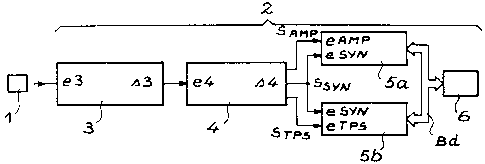
Fig. 1 diagrammatically shows the various means constituting the systemaccording to the invention and their interconnections, as well as the CdTe
detector to which the system is connected. In fig. 1 the CdTe detector is 1
and the elements constituting the system according to the invention is 2.
As shown in fig. 1, the output of the detector 1 is connected to the input
e3 of a charge preamplifier 3 ensuring the transformation of the information
coming directly from the detector 1 into an analog pulse which can be elec-
tronically processed. This charge preamplifier 3 includes a polarization
circuit. The preamplifier and the polarization circuit are of known types,
so that there is no need for a detailed description here.
The charge preamplifier 3 is connected by its output s3 to electronic meas-
uring means 4, which consist of an electronic card permitting biparametric
measurements, namely the amplitude of the pulse and its rise time. This
electronic card is called the "BIPAR card".
As will be explained hereina~ter, said electronic BIPAR card makes it pos-
sible to determine on the one hand the amplitude of the pulse from the
detector l and on the other the rise time of said pulse. At the output of
said electronic BIPAR card 4 are consequently obtained the three signals
necessary for the remainder of the processing, namely:
B lZ260.3 BM
- 6 - 2185091
- - an amplitude signal SAMp corresponding to the amplitude of the pulse from
the detector 1,
- a time signal STps indicating the rise time of the pulse from the detector
1 and
- a synchronization signal SSyN also emitted by the electronic card 4 in
order to synchronize all the processing operations to be carried out on
SAMp and STps.
The amplitude signal SAMp and the synchronization signal SSyN are both
supplied to an analog/digital coder (A/D), designated 5a. In parallel, the
time signal STps and the synchronization signal SSyN are transmitted to an
analog/digital coder 5b.
Each of the A/D coders 5a and 5b converts the analog signal received from
the electronic card 4 into a digital signal which can be processed by the
data processing means 6. These A/D coders 5a and 5b carry out conversions
of the signals SAMp and STps in synchronization with one another as a result
of the signal SSyN. The digital signals emitted by the A/D coders 5a and 5b
are then supplied to data processing means 6 by means of a data bus Bd.
According to the invention, each of the coders 5a and 5b has a RAM memory
in which are stored the data, i.e. the different signals SA~p and STps
received from the electronic card and to which the data processing means 6
can have access when they wish via the data bus Bd.
The data processing means 6 will process the data relative to the amplitude
and rise time of the pulse from the CdTe detector in order to quantify the
charge losses. These processings will be described in greater detail herein-
after.
The electronic BIPAR card 4 in fig. 1 is shown in greater detail in fig. 2.
This electronic card 4, which is connected, as was seen in fig. 1, to the
output s3 of the charge preamplifier 3, receives on its input e4 the analog
pulse from the charge preamplifier 3.
This electronic card 4 has an input circuit 7 into which is introduced the
B 12260.3 BM
~ 7 ~ 2 1 8 5 0 9 1
analog pulse from the preamplifier by means of a coaxial connecting cable.
The input e4 of the analog card 4 consequently also corresponds to the input
of the input circuit 7, whose function is to:
- adapt the input impedance of the electronic card 4 to a previously defined
value, which is advantageously 50 ohms, said impedance value being charac-
teristic of the coaxial cable connecting the charge preamplifier 3 to the
electronic BIPAR card 4, said impedance adaptation or matching having the
advantage of avoiding the appearance of an overvoltage on the transmitted
analog pulse;
- amplifying the analog pulse received with a predetermined gain so as to
obviate the losses linked with the adaptation, said amplification gain being
e.g. 5;
- choosing the polarity sign of the analog pulse as a function of the
polarity of the pulse from the charge amplifier, so that the processing
subsequently carried out is only performed on positive pulses.
In order to perform these functions, the input circuit 7 has an input ampli-
fier 8 ensuring the impedance matching to the previously defined value and
the amplification of the pulse supplied by the preamplifier. To the ampli-
fier 8 is connected an inverter 9 equipped with straps 9a, 9b, 9c in order
to optionally reverse the polarity sign.
The signal then obtained at the output s7 of the input circuit 7 is con-
sequently adapted so as to be processed by the amplitude circuit 10 and the
time circuit 18. It therefore acts simultaneously on two channels, namely
the amplitude channel 10 (or amplitude circuit 10) and the time channel 18
(or time circuit 18).
The first aim of the amplitude circuit 10 is permit the measurement of the
amplitude of the pulse from the detector in order to accurately acquire the
maximum of said pulse following a shaping optimizing the signal to noise
ratio.
This function of detecting the maximum of the pulse is ensured by two ele-
ments constituting the base of said amplitude circuit 10, namely a band
pass filter optimizing the signal to noise ratio and a peak detector.
B 12260.3 BM
- 8 - 2 1 8 5 0 9 1
- More specifically, the amplitude circuit 10 incorporates a C-R passive
differentiator 11 connected to the output s7 of the input circuit 7. This
differentiator 11 makes it possible to carry out a pseudo-pole-zero cancel-
lation so as to ensure a rapid return to the 0 V voltage level following
the passage of a pulse, which thus makes it possible to prepare the arrival
of the following pulse. For example, said differentiator 11 can have a
cutoff frequency of 234 kH at -3 dB and can be implemented on the basis of a
resistance of approximately 10 Kohms in parallel with a capacitance of
approximately 8.6 nF in order to implement the pole-zero cancellation func-
tion.
Connected to the output sll of the differentiator 11, the amplitude circuit10 has a low pass filter 12 permitting the optimization of the pulse signal
to noise ratio. According to the invention, the filter 12 is an order 8
BESSEL integrating filter with a cutoff frequency of 500 kH at -6 dB making
it possible to act on the pulse without causing an overvoltage on the latter.
The output s12 of the filter 12 is connected to two amplifier stages 13 and
14. More specifically, these gain amplifiers 13 and 14 have the function
of increasing the gain of the pulse to be processed, so as to permit a
more precise detection of the maximum of said pulse.
According to the invention, these amplifiers are inverting amplifiers, the
amplifier 13 having a gain A and the amplifier 14 a gain B. For information
purposes, the gain A of the amplifier 13 can be -4 and the gain B of the
amplifier 14 -5.75.
According to an embodiment of the invention, the second inverting amplifier
14 can incorporate an offset control.
The output s14 of the second gain amplifier 14 is connected on the one hand
to a peak detector 15 and on the other to a comparator 17, which supplies
a signal SPULSEA
The peak detector 15 makes it possible to acquire the maximum of the pulse
and is controlled by a logic TTL signal STDp supplied by the logic control
B 12260.3 BM
~ '
- 9- 2185091
- unit 30 to be described hereinafter. More specifically, when the signal
emitted by the logic unit 30 is at 1, the peak detector 15 is blocked at 0 V.
~ Conversely, if the signal emitted by the logic unit 30 is at 0, the peak
detector 15 is in the acquisition mode.
More specifically, the signal STDp emitted by the logic unit 30 controls two
transistors, which are not shown in the drawing in order not to overburden
it and namely a first transistor for zeroing the memory capacity and a
second transistor for avoiding the peak detector switching on noise, which
would then generate switching interference.
The output sl5 of this peak detector is connected to a sample and hold cir-
cuit 16 ensuring the storage of the maximum amplitude value. This sample
and hold circuit 16 is also controlled by the logic control unit 30 by a
signal SsHA.
At the output sl6 of said sample and hold circuit is obtained the amplitude
signal S~Mp representative of the maximum amplitude of the processed pulse.
This signal SAMp will subsequently be used by the data processing means 6
for determining the charge losses.
In parallel with the pea~ detector 15, the output s14 of said second gain
amplifier 14 is connected to a comparator 17. The latter ensures the com-
parison of the signal amplified by the amplifiers 13 and 14 with a low
threshold SB, which makes it possible to initiate the measurement of the
pulse and mark an absolute start pulse or cue for the determination of the
rise time. Thus, as shown in fig. 2, the signal SsB from the comparator
17 is supplied to the logic control unit 30, which is connected to the time
circuit 18, which thus permits the synchronization of the amplitude circuit
10 with the time circuit 18.
The rising front of the signal SsB is characteristic of the start of the
pulse rise time. The reception of said signal SsB by the logic unit 30
consequently conditions the remainder of the processing.
As explained hereinbefore, the output s7 of the input circuit 7 is connected,
B 12260.3 BM
-lO- 2185091
~ in parallel to the amplitude circuit 10, to the time circuit 18. The time
circuit 18 has a comparable architecture to the amplitude circuit 10, so
that only the novel or different elements will be described.
The time circuit 18 incorporates a differentiation circuit 19 connected to
the output s7 of the input circuit. Unlike the differentiator 11 of the
amplitude circuit 10, said differentiation circuit 19 has no pseudo-pole-
zero cancellation, because there is no need for the return to 0 V to be
precisely known. In the time circuit 18 the function of the differentiation
circuit 19 is to better mark the passage to the maximum of the pulse, which
is a vital time for said measurement.
According to an embodiment of the invention, said function is performed by
means of a double passive C-R filter and e.g. said filter can have a cutoff
frequency of 7.2 kHz at -6 dB.
The output S19 of the differentiation circuit 19 is connected to the input
e20 of a low pass filter 20. Advantgeously, said filter 20 is an order 8
BESSEB integrating filter and it has a similar function to the filter 12 of
the amplitude channel, but preferably has a cutoff frequency of approx-
imately 1 MHz at -6 dB in order to filter the noise without deteriorating
the original shape of the pulses.
It should be noted that the choice of filters is inter alia conditioned by
the time lags which they induce. The greatest time lag is caused by the
amplitude channel, which includes the lowest frequency filter. However,
unlike that of the amplitude channel, the time channel filter must not have
a too high low cutoff frequency otherwise it will authorize peak detections
following the passage of the peak on the time channel.
In the same way as for the amplitude channel 10, the output s20 of the low
pass filter 20 is connected to two inverting amplifier stages 21 and 22
of respective gains A and B. According to an embodiment, the gain A of the
amplifier 21 is -2 and the gain B of the amplifier 22 is -3.75.
At the output s22 of the second amplifier stage, i.e. of gain amplifier 22,
B 12260.3 BM
11 21-85091
- the pulse is on a continuous level of 1 V. The control of this continuous
voltage can be implemented by means of a potentiometer or a divider bridge,
- whose calculation is optimized as a function of the offset voltages.
The output s22 of these inverting amplifiers 21 and 22 is connected to a
peak detector 23, whose basic operation is identical to the peak detector
15 of the amplitude channel 10.
However, this peak detector 23 is used differently as compared with the case
of the amplitude channel 10. Thus, for the time channel 18, it is used so
as to determine the end of the rise time of the pulses. This makes it
possible to operate on both slow or fast pulses (for our application, the
gamma of the rise times is between 500 ns and 8 ,us) and independently of
their shapes. In other words, this circuit is automatically adapted to the
low frequency part of the spectrum of the pulses, which is more or less
extensive as a function of the charge losses.
In order to optimize the operation of the peak detector 23, a modification
is necessary by the addition of a resistor and a capacitor, compared with
the standard, known diagram of the peak detector 15. For example, the
values of these components can respectively be approximately 10 Kohms and
33 pF.
In said time circuit 18, the function of the peak detector 23 is to supply
the end of pulse rise time information. These are properties of internal
signals STAs and STsO of said peak detector 23 in the acquisition phase
making it possible to acquire such an information. STAs is the control sig-
nal of the peak detector 23 and STsO tlle output signal equal to the maximum
voltage of the pulse at the input e23 of the peak detector 23. Thus, when
the pulse is in the rise phase, the voltage signal STsO is below the voltage
signal STAs. However~ the passage to the maximum of the pulse gives rise
to a change in the voltages, i.e. STsO hecomes higher than STAs. Thus,
said two voltage signal STsO and STAs are introduced into a comparator 24,
which carries out the comparison between said two signals in order to estab-
lish whether, as explained hereinbefore, STsO exceeds STAs. Determination
then takes place to establish if the pulse is in the rising phase or has
B 12260.3 BM
2 1 850~1
reached its maximum.
- The output s24 of the comparator 24 is connected to one of the inputs of
the logic control unit 30 and supplies a logic signal SFTM, whose rising
front marks the rise time end.
The logic control unit 30 is also connected to the peak detector 23 of the
time circuit, in the same way as for the peak detector 15 of the amplitude
circuit 10. Thus, it supplies to the two peak detectors 15 and 23 the same
logic signal STDp ensuring their synchronization.
The logic unit 30 can also supply the comparator 24 with another logic
signal St making it possible to block the signal SFTM at 0 at the start
of the measurement in order to avoid interfering transient voltages.
According to the invention, the amplitude channel 10 and time channel 18 are
designed so that their joint operation permits the measurement of the rise
time on the one hand and on the other an amplitude measurement coherent with
that of the rise time with a view to a mathematical processing. It is then
said that these two channels are coupled. This coupling makes it possible
to determine the pulse rise time on the basis of the determination of the
rising fronts of the signal SsB (clearing the low threshold) of the ampli-
tude channel 10 and the signal SFTM (pulse marking the rise time end) of the
time channel 18. Thus, the pulse rise time is determined indirectly due on
the one hand to the signal SsB ~easured on the amplitude channel 10 and
the other to the signal SFTM measured on the time channel 18. These two
data relative to the clearing of the low threshold and the pulse or cue mar-
king the end of the rise time are both fed to the logic control unit 30,
which returns said informations to a threshold/ramp circuit 25.
The coupling of said two time and amplitude channels makes it possible to
obtain freedom from the very varied shapes which the pulses can have when
supplied by CdTe detectors. As a result of a narrow band pass filter, the
amplitude channel 10 leads to a constant pulse shape. Thus, the start pulse
marked by the signal SsB for the rise time measurement corresponds to a same
starting reference for all the pulses which have to be processed by the
B 12260.3 BM
- 13 - 2185091
- system. Moreover, the time channel 18, due to a wide band pass filter,operates with respect to the real shape of the voltage in such a way as to
- detect the real end of the pulse rise time and thus take account of charge
loss variations.
Thus, the coupling of these amplitude and time channels makes it possible to
indirectly electronically measure the pulse rise time by means of an infor-
mation representative of said rise time.
As stated hereinbefore, the BIPAR electronic card incorporates a circuit 25
known as a threshold/ramp circuit, which has on the one hand a voltage
source 26 supplying the complete BIPAR card with reference voltages used in
the comparators 17 and 29. A reference voltage SB known as the low thresh-
old is in particular used in the comparator 17, where it is compared with
the signal SpuLsEA. This voltage source 26 also supplies a reference volt-
age SS called the security threshold and whose use will be described herein-
after. According to an embodiment of the invention, said reference voltage
source incorporates accessible potentiometers on which it is possible to
effect chosen threshold controls. The threshold/ramp circuit 25 also has a
ramp circuit 27 receiving at lts input e27 a signal STR emitted by the logic
control unit 30. When said signal STR is at 0, a constant current generator
linearly charges a capacitor, but when the signal STR is at 1, said same
capacitor is forced to 0 V.
The ramp circuit 27 also has an inverting gain amplifier connected to the
capacitor and which can e.g. have a gain of -6.45.
The signal then obtained at the output s27 of the ramp circuit 27 is a sig-
nal, whose linear portion is representative of the pulse rise time.
A control or setting of the continuous starting voltage of the ramp circuit
27 makes it possible to tune the ramp in a window compatible with that of
the analog/digital coder 5b connected to the output s28 in order to digiti~e
the rise time signal.
According to a variant of the invention, the voltage ramp obtained as a
B 12260.3 BM
'--
21 85091
- result of the constant current generator of the circuit 27 is regulatable,
which permits an adaptation to different converter types.
The signal obtained in this way at the output s27 of the ramp circuit 27 is
introduced into a sample and hold circuit 28 which, in the acquisition mode,
follows the ramp and, following a rising front of the signal SFTM, stores
the value in the ramp when the signal SsHR from the control logic 30, com-
mands it.
At the output s28 of the sample and hold circuit 28 is then obtained the
signal STps representative of the rise time of the pulse from the CdTe
detector.
To the output s27 of the ramp circuit 27 is also connected a comparator 29
ensuring a comparison between the signal at s27 from the ramp 27 and a
security threshold SS supplied by the reference voltage circuit 26. This
makes it possible to fix a maximum limit of the rise time (to increase the
resolution quality of the spectrum) or detect interfering events such as
noise, which can trigger the low threshold SB, but not the end of the rise
time SFTM. Tne comparator 29 generates a logic signal SsR, which is supp-
lied to the logic control unit 30, which controls all the circuits described
hereinbefore.
Unit 30 more particularly has the following functions. It ensures the
sequencing of the operations during a normal measurement and in particular
the operation of detecting the clearing of the low threshold SB and the
passage into the measuring mode. It also ensures the acquisition of the
rise time and the amplitude maximum, the storage of the data in the sample
and hold circuits and the digital conversion request by the synchronlzation
square wave pulses SSyN connecting the electronic BIPAR card to the A/D
converters shown in fig. 1. It detects the stacks, whilst monitoring the
low threshold. This function is conditioned by the separation performance
characteristics of the filter 12 with respect to the amplitude channel 10.
The term "stack" is used for the result of two gamma interactions leading to
an overlap of the first pulse by the second pulse from the CdTe detector. It
also monitors the base line, i.e. checks whether the voltage of 0 V is
B 12260.3 BM
21 85091
- stable. When a measurement is ended, the logic control unit 30 checks that
a pulse is not present before authorizing a new cycle, so as to ensure that
~ said cycle will start from a "proper" base line. In the opposite case, the
logic unit 30 will decide on a waiting procedure to be carried out until the
normal measuring mode is again possible. It carries out the control of the
signal SsR marking the upper limit of the ramp.
Fig. 3 shows various timing diagrams revealing the different signal encoun-
tered within the BIPAR electronic card and which are mostly controlled by
the logic control unit 30.
On channel A of fig. 3 is shown the pulse, such as is obtained at the out-
put s22 of the double amplifier stage 21, 22 of the time channel 18, i.e.
the pulse occurring at the input e23 of the peak detector 23.
On channel B curve Cl represents the signal obtained at the output sl4 of
the double amplifier stage 13 and 14 of the amplitude channel 10, i.e. the
signal occurring at the input el5 of the peak detector 15. The mixed line
curve represents the low threshold voltage SB. Curve C2 represents the sig-
nal S~p obtained at the output of the amplitude channel 10, i.e. the signalrepresenting the maximum amplitude of the pulse from the CdTe detector.
This signal is offset or staggered by a time lag R compared with the signal
of channel A. All the signals C to K will be offset by said time lag R
compared with the signal of channel A.
On channel C of fig. 3 is shown the curve C3 corresponding to the signal
STAs obtained at the output s23 of the peak detector 23, as well as the
curve C4 corresponding to the signal STsO obtained at the same output of the
peak detector 23.
On channel D of fig. 3 is shown by means of curve C5, the ramp signal
obtained at the output s27 of the ramp circuit 27 and curve C6 represents
the rise time signal STps obtained at the output s28 of the BIPAR electronic
card.
On channel E of fig. 3 is shown the shape of the signal SsB obtained at the
B 12260.3 BM
- 16 - 2 1 8 5 0 9 1
- output sl7 of the comparator 17 of the amplitude channel 10.
- On channel F is represented the signal STDp supplied by the logic control
unit 30 to each of the peak detectors 23 and 15.
Channel G of fig. 3 shows the signal SFTM obtained at the output s24 of the
comparator 24 of the time channel 18.
Channel H of fig. 3 shows the signal STR supplied by the logic control unit
30 to the ramp circuit 27.
Channel I of fig. 3 shows the signal SsHR emitted by the logic control unit
30 and supplied to the sample and hold circuit 28.
Channel J of fig. 3 shows the signal SsHA supplied by the logic control unit
30 to the sample and hold circuit 16.
Channel K of fig. 3 represents the synchronization signal SSyN supplied by
the logic control unit 30 to the analog/digital converters 5a and 5b in order
to permit a synchronization during the digitizing of the amplitude signal
SAMp and rise time signal STps.
On considering these various timing diagrams, it will be seen that when a
pulse appears at the input of the BIPAR electronic card, the rising front of
the signal SsB initiates a measurement, which brings about the zeroing of
the signal STDp, as well as the signal St . The rising front of the signal
SFTM then brings about the storage of the ramp value at this time on the
order of the signal SsHR and then the amplitude value on the order of the
signal SsHA. Immediately, the signal STR is set to 1, which again brings
the ramp to 0. A clock with a chosen period of e.g. 6 ,us is then authorized
to sequence the emission of rise time and amplitude signals to the analog/
digital coders, which represents the generation of the signal SSyN.
According to a variant of the invention, a delay line is inserted in the
time channel 18 in order to permit the use of frequencies of filters
incompatible in phase shift terms, the propagation time of the time channel
B 12260.3 BM
21 85091
being smaller than that of the amplitude channel 10.
- According to another variant of the invention, specific base line restora-
tion and stack detection circuits can be added, which have better perform-
ance characteristics than those implemented by the logic control unit 30.
Such a variant makes it possible to increase the counting frequency of the
BIPAR electronic card.
According to yet another variant, whilst retaining the same BIPAr electron-
ics architecture, the filter cutoff frequencies, the amplifier gains, the
control of the peak detector 23 of the time channel 18 and the gradient of
the ramp 27 can be modified in order to adapt to detector types other than
CdTe detectors, for which the simultaneous measurement of the amplitude and
the rise time has an interest.
According to another variant, whilst significantly complicating the ampli-
tude channel 10 and the time channel 18, the electronic BIPAR card could
proces bipolar pulses.
As has been seen in fig. 1, the analog/digital converters 5A and 5B are
connected by means of a data bus Bd to data processing means 6 of the PC
type.
~oreover, as explained hereinbefore, the BIPAR electronic card makes it
possible to determine a measurement of the amplitude and the rise time of
the pulse coming from the CdTe detector with a view to determining the corr-
ection of the detector charge loss. It is this charge loss correction which
is determined by means of the computer 6, because the relation between the
rise time and the charge loss is not immediate. Thus, the relation between
the rise time and the charge loss is dependent both on the electronics and
the CdTe detector used. It is therefore necessary to carry out a calibra-
tion for each detector. According to the invention, the data processing
means 6 consequently make it possible to determine the "amplitude/rise time"
relation for each detector and for a given BIPAR electronics.
The calibration process consists of measuring, for each pulse rise time,
B 12260.3 BM
- 18 - 2 1 8 5 0~ 1
- the detector response to calibrated stresses, i.e. lines of known radio-
active elements. Two lines can be sufficient to obtain a satisfactory
- correction.
In order to measure the detector response for all the rise times, it is
necessary for said two lines to have a certain minimum energy, in order to
bring about a depth penetration of the crystal of each detector, but at the
same time not an excessive energy, so that the calibration time is not too
long. In other words, the calibration of the device consists of exposing
the detector which it is wished to use to a mixture of these two sources
and then record the number of events received for each amplitude and rise
time.
For example, for detectors having crystals with a thickness of 2 mm, the
57Co line at 122 KeV and 133BA line at 356 KeV are completely satisfactory.
These two elements also have the advantage of relatively long life periods.
More specifically, the data processing and calibration process used by the
data processing means 6 operates in the following way:
- the data are represented in an amplitude/time diagram, where the abscissa
axis is the axis of the amplitudes and the ordinate axis the time axis,
- for each rise time, the spectrum of the amplitude lines is plotted,
- in the calibration phase, the process consists of automatically calculat-
ing a mathematical law representative of the variation of the maximum of the
lines as a function of the energy and the rise time, in accordance withmathematical criteria dependent on the desired precision,
- in the normal measurement phase, the correction law deduced from the cali-
bration is directly applied to the data read in to the memory.
Fig. 4A shows in an amplitude/rise time/event number diagram, where the
x axis comprises 1024 channels and the z axis 512 channels, the number of
events received for each amplitude and rise time. On the basis of this plot
dotted lines show the positions of the maxima corresponding to the energies
E1 and E2. These positions were transferred to fig. 4B, which is a diagram
of the rise time as a function of the amplitude. For each rise time, start-
ing from the shortest times, the first significant maxima are sought. For
B 12260.3 BM
- 19 ~ 2 1 8 ~09 1
- each longer rise time, definition takes place of two regions of interest,
each corresponding to lines, based on the results obtained for the immedi-
- ately lower rise time.
This operation consists of determining the positions of the maxima Clt and
C2t, as well as the width of the lines in these regions of interest for each
rise time t. This is followed by the calculation of the gain and offset
correction parameters in the following way:
GAIN (t) = (E2 - E1)/(C2t - Clt) ;
OFFSET (t) = (El - GAIN (t) x Cl ).
These parameters are then recorded in a file, which constitutes the calibra-
tion file of the detector. It is thus possible to carry out a series of
measurements with the same detector without having to recommence the
operation, because the necessary data have been stored during the initial
calibration.
Any change of detector requires a new calibration, unless the new detector
has already been calibrated. If radioactive calibration sources are not too
prejudicial with respect to the measurement, the calibration and measurement
stages can be simultaneous.
More specifically, this operation consists of carrying out a maximum searcll
in a region of interest (Nl, ~2) of the spectrum. The spectrum is smoothed
by taking a current mean relating to a number DIM of channels, in which DIM
= (N2 - Nl)/4.
The derivative D of the smoothed spectrum (SL) is then calculated:
D(i) = SL(i f DIM/2) - SL(i - DIM/2).
The passage from O to D is obtained by linear interpolation between the
two channels surrounding it, said value being the position of the line. The
positions of the right and left extremes of D make it possible to estimate
the total, mid-height width of the peak of the line (FWHM), by applying a
B 12260.3 BM
- 20 ~ 21 85091
- relation dependent on the dimension of the region of interest:
FWHM = [RIGHT - LEFT] - O.87 x (DIM/2) ,
the LEFT and RIGHT values obtained at time t-l defining the limits Nl and N2
of the region of interest at time t.
The process implemented by said data processing means consists of correcting
any subsequent measurement on the basis of the data of the calibration file
in order to generate a corrected spectrum with respect to the charge losses.
This operation consists of redistributing the events measured in the channel
C with the rise time t between the energies:
GAIN (t) x c + OFFSET (t)
and
GAIN (t) x (c + 1) + OFFSET (t).
Any subsequently performed measurement using the calibrated detector can
then be corrected in the same way in real time or deferred time.
The previously described correction process can obviously be simplified by
using a single calibrated spectrum line, obviously this being detrimental
to the precision. However, it is also possible to use more than two spec-
trum lines, so as to further increase the calibration precision.
This process can also be performed on digitized measurements of the ampli-
tude and rise time of pulses supplied by a detector having charge losses,
in the case where said measurements would be supplied by an electronic appar-
atus other than a BIPAR electronic card, e.g. the apparatus manufactured by
EURORAD and referred to under "Prior art" in the present text.
The device according to the invention, adapted to a high quality CdTe detec-
tor, makes it possible to obtain a simple system, which is flexible in use,
easily transportable, relatively inexpensive and having very good spectro-
scopic performance characteristics.
It also makes it possible to implement a camera gamma without photomulti-
pliers and therefore with all the resulting material gains. This camera
B 12260.3 BM
- 21 ~ 21 85091
- gamma can be used in numerous fields, i.e. medical imaging, the control and
dismantling of nuclear power stations, gamma astronomy, etc.
B 12260. 3 BM