Note: Descriptions are shown in the official language in which they were submitted.
2185955
DIELECTRIC RESONATOR CAPABLE
OF VARYING RESONANT FRl?QUENCY
The present invention relates to a dielectric resonator
capable of varying its resonant frequency for use in a microwave or millimeter
wave
band.
A demand for mobile communication systems in 900 MHz
and quasi-microwave bands has increased rapidly in recent years and a future
deficiency of usable frequencies is therefore apprehended. Systems adapted to
multimedia communications such as communication s~,rstems for transmitting
images
or image information are being studied. Such conununication systems must be
realized as large-capacity high-speed communication systems. The use of
millimeter wave frequency bands which are practically unused and in which the
band width and the capacity of a communication channel and the communication
speed can easily be increased has been taken into consideration.
Conventionally, cavity resonators have generally been used
as microwave and millimeter wave band filters for use in oscillators and
filters.
Recently, however, cylindrical TEo,a mode dielectric resonators have come into
wide use in place of high-priced large cavity resonators. In 1975, a practical
TEo,a
mode dielectric resonator of this kind was made having high stability with
respect
to temperature by using a temperature-characteristic-compensated dielectric.
In
general, the temperature characteristics of TEo,a mode dielectric resonators
are
determined by the temperature characteristics of the material of the
resonator.
218595
'Therefore, TEo,a mode dielectric resonators have the advantage of being free
from
the need for using an expensive metal such as Kovar or Invar to form the
cavity.
Also, variable frequency dielectric resonators have recently
been studied for use in voltage controlled oscillators, for example.
Fig. 13 is a perspective view of a conventional variable
frequency dielectric resonator constructed by using a TEo,a mode dielectric
resonator
301. This variable frequency dielectric resonator consists of a variable
frequency
microstrip line resonator MR350 having a varactor diode 304, and the TEola
mode
dielectric resonator 301. That is, on an upper surface of a dielectric
substrate 306
having a grounding conductor 307 formed on its lower surface, a strip
conductor 302
and a strip conductor 303 are formed so that one end of the strip conductor
302 and
one end of the strip conductor 303 face each othc;r with a predetermined
spacing.
The strip conductor 302 and the grounding electrode 307 between which the
dielectric substrate 306 is interposed form a microstrip line resonator MR302
while
the strip conductor 302 and the grounding electrode 307 between which the
dielectric substrate 306 is interposed form a micros,trip line resonator
MR303. The
varactor diode 304 is connected in series between the strip conductors 302 and
303.
Thus, the variable frequency microstrip line resonator MR350 is constituted of
the
microstrip line resonators MR302 and MR303 and the varactor diode 304.
The TEo,a mode dielectric resonator 301 is placed on the
upper surface of the dielectric substrate 306 close to the strip conductor
302. The
TEola mode dielectric resonator 301 and the variable frequency microsh-ip line
resonator MR350 are thereby coupled with each other electromagnetically, thus
constructing the conventional variable frequency dielectric resonator
constituted of
the TEo,a mode dielectric resonator 301 and the variable frequency microstrip
line
resonator MR350.
2
2185955
The strip conductor 305 formed on the upper surface of the
dielectric substrate 306 is placed close to the TEo,a mode dielectric
resonator 301,
thereby constructing the microstrip line M305 which is constituted of the
strip
conductor 305 and the grounding conductor 307 with the dielectric substrate
306
interposed therebetween and which is electromagnetically coupled with the
variable
frequency dielectric resonator.
In the thus-constructed conventional variable frequency
dielectric resonator, the resonance frequency is variable by changing the
electrostatic capacity of the varactor diode 304. The electrostatic capacity
of the
varactor diode 304 is changed by changing a reverse bias voltage applied to
the
varactor diode 304. Also, an external circuit, e.g., a negative resistance
circuit or the
like can be connected to the resonator through the; microstrip line M305.
A variable resonance frequency type of cavity resonator
may also be made by providing a varactor diode in a portion of a cavity or by
being
arranged so that the size of a cavity is changeable.
The conventional variable frequency dielectric resonator
constructed by using the TEo,d mode dielectric resonator 301, however, has a
complicated structure and is high-priced because tlhe two resonators, i.e.,
the TEo,d
mode dielectric resonator 301 and the variable frequency microstrip line
resonator
MR350, are used. Also, the resonance frequency of the conventional variable
frequency dielectric resonator cannot easily be' adjusted. Further, since the
conventional variable frequency dielectric resonator is constructed by using
the two
resonators: the TEo,d mode dielectric resonator :301 and the variable
frequency
microstrip line resonator MR350, not a simple single mode but two modes, i.e.,
an
even mode and an odd mode, occur. Therefore, if the conventional variable
frequency dielectric resonator is used in an oscillator, a mode jump can occur
easily
from a desired resonance mode to a resonance mode different from the desired
3
2185955
resonance mode to cause oscillation at a resonance frequency different from
the
desired resonance frequency. Also, cavity resonators of the variable resonance
frequency type are disadvantageously large in si2;e and high-priced.
In view of the above-described problems, an object of the
present invention is to provide a variable frequency dielectric resonator
capable of
easily adjusting a resonance frequency, reducing occurrence of a mode jump
when
used in an oscillator and being manufactured at a lower cost in comparison
with the
conventional variable frequency dielectric resonator.
To achieve this object, according to one aspect of the
present invention, there is provided a variable frequency dielectric resonator
capable
of resonating at a resonance frequency, comprisW g a dielectric substrate
provided
between two conductor plates facing each other and having a first surface and
a
second surface opposite from each other, a first electrode formed on the first
surface
of the dielectric substrate and having a first opening formed in a
predetermined
shape over a central portion of the first surface ~of the dielectric
substrate, and a
second electrode formed on the second surface of tl~ie dielectric substrate
and having
a second opening formed in substantially the same shape as the first opening
and
positioned opposite from the first opening. Spacing between the dielectric
substrate
and the conductor plates and a thickness and a dielectric constant of the
dielectric
substrate are set such that the portion of the dlielectric substrate other
than a
resonator formation region between the first opening and the second opening,
interposed between the first and second electrodes, attenuates a high-
frequency
signal having the same frequency as the resonance frequency. The variable
frequency dielectric resonator also comprises a slit formed in at least one of
the first
and second electrodes so as to connect with the corresponding one of the first
and
second openings, a third electrode formed in thc; slit in such a manner as to
be
insulated from the first and second electrodes, and a~ variable capacitance
connected
between the first or second electrode and the third electrode in the vicinity
of the
4
2185955
position at which the first or second opening connects with the slit, the
electrostatic
capacitance thereof being variable according to a change in a voltage applied
between the first or second electrode and the third electrode. The resonance
frequency of the dielectric resonator is changed lby changing the voltage
applied
between the first or second electrode and the third electrode.
According to another aspf:ct of the present invention, in the
above-described variable frequency dielectric resonator, the variable
capacitance has
a fixed electrode and a movable electrode each forrr~ed as a thin-film
conductor. The
fixed electrode and the movable electrode are supported on an insulating base
so as
to face each other through a cavity formed in the :insulating base.
According to still another aspect of the present invention,
in the above-described variable frequency dif;lectric resonator, the variable
capacitance comprises a varactor diode.
These and other objects., features and advantages of the
present invention will become apparent from the i:ollowing detailed
description of
embodiments of the invention with reference to the accompanying drawings.
A presently preferred embodiment of the present
invention will now be described, by way of example only, with reference to the
accompanying drawings, in which:
Fig. 1 is a cross-sectional view of a variable frequency
dielectric resonator 81 which represents a first embodiment of the present
invention;
Fig. 2 is a longitudinal sectional view taken along the line
A-A' of Fig. 1;
~~85955
Fig. 3 is a longitudinal sectional view of a TEo,o mode
dielectric resonator 81 a for explanation of the principle of resonance in the
variable
frequency resonator 81 shown in Fig. 1;
Fig. 4 is a longitudinal sectional view of a dielectric
substrate 3 for explanation of the principle of resonance in the TEolo mode
dielectric
resonator 81a shown in Fig. 3;
Fig. 5 is a circuit diagram showing an equivalent circuit of
the TEo,o mode dielectric resonator 81a shown in Fig. 3;
Fig. 6(a) is a longitudinal sectional view of a TEo,o mode
dielectric resonator 81b which was used as a model for analyzing the operation
of
the TEo,o mode dielectric resonator 81a shown in Fig. 3;
Fig. 6(b) is a cross-sectional view taken along the line B-B'
of Fig. 6(a).
Fig. 7 is a graph showing the relationship between the
resonance frequency and the diameter d of a resonator formation region 63 in
the
TEo,o mode dielectric resonator 81a shown in Fig. 3;
Fig. 8 is a longitudinal sectional view of an electric field
strength distribution in the longitudinal sectional ~~iew of Fig. 6(a);
Fig. 9 is a longitudinal sectional view of a magnetic field
strength distribution in the longitudinal sectional view of Fig. 6(a);
6
2185955
Fig. 10 is a cross-sectional view of a variable frequency
dielectric resonator 82 which represents a second embodiment of the present
invention;
Fig. 11 is a longitudinal sectional view of variable
capacitors 90a and 90b shown in Fig. 10;
Fig. 12 is a circuit diagram showing an equivalent circuit
of the variable frequency dielectric resonator 81 shown in Fig. 1; and
Fig. 13 is a perspective view of a conventional variable
frequency dielectric resonator.
<First Embodiment>
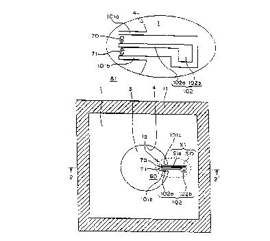
Figs. 1 and 2 are a cross-sectional view and a longitudinal
sectional view, respectively, of a variable frequency dielectric resonator 81
which
represents a first embodiment of the present invention. Fig. 1 shows a section
along
a lateral plane between a varactor diode 70 and an upper conductor plate 211.
As shown in Figs. 1 and 2, the variable frequency dielectric
resonator 81 of the first embodiment has a resonator formation region 60
formed in
a central portion of the dielectric substrate 3 provided between upper and
lower
conductor plates 211 and 212 opposed to each other. The resonator formation
region 60 is defined between an opening 4 formed in a central portion of an
electrode 1 and an opening 5 formed in a central portion of an electrode 2.
The
electrode 1 is formed on the upper surface of the dielectric substrate 3 while
the
electrode 2 is formed on the lower surface of the dielectric substrate 3.
A slit S 1 is formed in the electrode 1 so as to connect with
the opening 4. A bias electrode 102 is formed in the slit S 1 so as to have an
end
7
X2185955
projecting into the opening 4. Electrodes lOla and lOlb are provided on the
opposite sides of the bias electrode 102. Each o~F the electrode lOla and lOlb
is
formed close to the bias electrodes 102 so as to have one end opposed to the
end of
the bias electrode 102 projecting into the opening 4 and to have the other end
connected to the electrode 1.
A varactor diode 70 is connected between the
corresponding opposed end of the electrode 101 a amd the end of the bias
electrode
102 while a varactor diode 71 is connected betwef:n the end of the electrode
lOlb
and the corresponding opposed end of the bias electrode 102. A predetermined
direct current voltage is applied between the electrodes lOla and lOlb and the
bias
electrode 102 to apply a reverse bias voltage bel:ween the two terminals of
the
varactor diodes 70 and 71. The resonance frequency of the dielectric resonator
can
be varied by changing the reverse bias voltage.
The variable frequency dif:lectric resonator 81 of the first
embodiment will now be described in more detail with reference to the
drawings.
As shown in Figs. 1 and 2, the electrode 1 is formed on the
upper surface of the dielectric substrate 3 provided between the upper and
lower
conductor plates 211 and 212 opposed to each other, and the circular opening 4
having a diameter d is formed over a central portion of the upper surface of
the
dielectric substrate 3. Also, the electrode 2 having; the opening 5 having the
same
configuration as the opening 4 is formed on the lower surface of the
dielectric
substrate 3. The dielectric substrate 3 has a predetermined dielectric
constant and
has a square shape each side of which has a length D. The diameter d of the
opening 4 and 5 is smaller than the length of each side of the dielectric
substrate 3,
and the opening 4 and 5 are formed so as to be coaxial with each other.
B
2185955
A cylindrical resonator formation region 60 is defined in the dielectric
substrate 3 with these openings. The resonator formation region 60 is a
cylindrical region
formed at the center of the dielectric substrate 3 and has an upper end
surface 61 on the
opening 4 side and a lower end surface 62 on the opening 5 side. The resonator
formation
region 60 also has a virtual circumferential surface 360 formed in the
dielectric substrate 3.
The distance between the dlielectric substrate 3 and the upper conductor
plate 211, the distance between the dielectric sut~strate 3 and the lower
conductor plate 212,
the dielectric constant and the thickness t of the dielectric substrate 3 and
the diameter d of the
openings 4 and 5 are set to such values that a standing wave occurs when a
high-frequency
signal having the same frequency as the resonance frequency of the vauiable
frequency
dielectric resonator 81 is input to the resonator formation region 60.
The electrode 1 is formed on the entire area of the upper surface of the
dielectric substrate 3 except for the upper end surface 61 while the electrode
2 is formed on
the entire area of the lower surface of the dielectric substrate 3 except for
the lower end surface
62. An annular portion of the dielectric substrate 3 other than that in the
resonator formation
region 60 is interposed between the electrodes 1 aand 2 to form a parallel-
plate waveguide. The
dielectric constant er and the thickness t of the dielectric substrate 3 are
set to such values that
a cut-off frequency of this parallel-plate wavegu:ide in a TEo,o mode which is
a fundamental
propagation mode of the parallel-plate waveguidle is higher than the resonance
frequency of
the TEo~o mode dielectric resonator 81. That is, the annular portion of the
dielectric substrate
3 other than the resonator formation region 60, interposed between the
electrodes 1 and 2,
forms an attenuation region 203 for attenuating; a high-frequency signal
having the same
frequency as the resonance frequency. In other words, the dielectric constant
er and the
thickness t of the dielectric substrate
9
?_ 185955
3 are selected so that the attenuation region 203 attenuates a high-frequency
signal
having the same frequency as the resonance frequency.
The slit S 1 is formed in the electrode 1 so as to connect
with the opening 4. The slit S 1 is formed of a strip electrode formation slit
S 1 a
which is defined by a predetermined length from its end open to the opening 4,
which length is sufficiently larger than its width, and a terminal electrode
formation
slit S lb which is formed into a generally square shape and one side of which
has a
length larger than the width of the strip electrode formation slit S 1 a. The
slit S 1 is
formed so that the lengthwise direction of the drip electrode formation slit S
la
coincides with the direction normal to a circle defining the circumference of
the
opening 4.
The bias electrode 102 is formed by connecting a terminal
electrode 102b having a generally square shape and provided for connection to
a
bias conductor wire (not shown) and a strip electrode 102a smaller in width
than the
terminal electrode 102b and having a length sufficiently larger than its
width. The
bias conductor wire has its one end connected to the terminal electrode 102b
and the
other end connected a variable voltage DC power source through a high-
frequency
coil or the like, for example. The bias electrode 102 is formed in the slit S
1 while
being insulated from the electrode 1. The bias electrode 102 is formed so that
the
terminal electrode 102b is positioned in the termiinal electrode formation
slit Slb,
and so that the lengthwise direction of the strip electrode 102a is parallel
to the
lengthwise direction of the electrode formation slit S 1 a, with one end of
the strip
electrode 102a projecting in the opening 4.
The electrodes lOla and lOlb are formed parallel to the
strip electrode 102a on the opposite sides of the strip electrode 102a so that
one end
of each of the electrodes lOla and lOlb is opposed to the projecting end of
the strip
electrode 102a, with the other end of each of the electrodes lOla and lOlb
connected to the electrode 1 in the vicinity of the position at which the slit
S 1 and
the opening 4 meet each other. The varactor diode 70 is connected between the
projecting ends of the electrode l0lb and the strip electrode 102a while the
varactor
diode 71 is connected between the projecting ends of the electrode lOlb and
the
strip electrode 102a. The cathode terminal of the varactor diode 70 is
connected to
the strip electrode 102a while the anode terminal of the varactor diode 70 is
connected to the electrode lOla. Also, the cathode terminal of the varactor
diode
71 is connected to the strip electrode 102a while flue anode terminal of the
varactor
diode 71 is connected to the electrode lOla.
The dielectric substrate 3 with the electrodes 1 and 2 is
provided in a cavity 10 formed in a conductor case 1 l, as described below.
The
conductor case 11 is formed by square upper and lower conductor plates 21 l
and
212 and four side conductors. Inside the conductor case 11, the cavity 10 is
formed
as a square prism having a height h and a square cross section each side of
which
has a length D. The dielectric substrate 3 is placed in the cavity 10 so that
the side
surfaces of the dielectric substrate 3 contact the <.~ide conductors of the
conductor
case 11, and so that the distance between the upper surface of the dielectric
substrate
3 and the upper conductor plate 211 of the conductor case 11 and the distance
between the lower surface of the dielectric substrate' 3 and the lower
conductor plate
212 of the conductor case 11 are equal to each other and approximately equal
to a
distance hl shown in Fig. 2, which is the distance between the surface of the
electrode 1 or 2 and the upper or lower conductor plate 211 or 212. A free
space
formed between the electrode 1 and the portion of the upper conductor plate
211
other than the portion of the same facing the upper end surface 61 of the
dielectric
substrate 3 forms a parallel-plate waveguide. The distance hl is set to such a
value
that a cut-off frequency of this parallel-plate wave;;uide in a TEolo mode
which is
a fundamental propagation mode of this parallel-plate waveguide is higher than
the
resonance frequency. That is, the free space between the electrode 1 and the
portion
of the upper conductor plate 211 other than the portion of the same facing the
upper
11
X185955
end surface 61 of the dielectric substrate 3 forms an attenuation region 201
for
attenuating a high-frequency signal having the s~une frequency as the
resonance
frequency. In other words, the distance h 1 is selected so that the
attenuation region
201 attenuates a high-frequency signal having the same frequency as the
resonance
frequency.
Similarly, a free space formed between the electrode 2 and
the portion of the lower conductor plate 212 other than the portion facing the
lower
end surface 62 of the dielectric substrate 3 forms a parallel-plate waveguide.
The
distance hl between the electrode 2 on the dielectric substrate 3 and the
lower
conductor plate 212 of the conductor case 11 is set to such a value that a cut-
off
frequency of this parallel-plate waveguide in a TE,"o mode which is a
fundamental
propagation mode of this parallel-plate waveguide is higher than the resonance
frequency. That is, the free space between the electrode 2 and the portion of
the
lower conductor plate 212 other than the portion of the same facing the lower
end
surface 62 of the dielectric substrate 3 forms an attenuation region 202 for
attenuating a high-frequency signal having the same frequency as the resonance
frequency. In other words, the distance hl is selected so that the attenuation
region
202 attenuates a high-frequency signal having the same frequency as the
resonance
frequency. The variable frequency dielectric resonator 81 of the first
embodiment
is thus constructed.
The operation of the variable frequency dielectric resonator
81 of the first embodiment constructed as described above will now be
described.
The principle of resonance in the variable frequency dielectric resonator 81
can be
explained in the same manner as the principlf; of resonance in a TEo,~ mode
dielectric resonator 81a which is constructed b~y removing the slit S1, the
bias
electrode 102, the electrodes lOla and lOlb and the varactor diodes 70 and 71
from
the variable frequency dielectric resonator 81. Therefore, the principle of
resonance
in the TE~,o mode dielectric resonator 81a will first be described with
reference to
12
Z~$59~~
Figs. 3 to 9 and the principle of changing the resonance frequency of the
variable
frequency dielectric resonator 81 will next be described.
In the TEo,o mode dielectric resonator 81a shown in Fig.
3, a resonator formation region 60 in which a standing wave occurs when a
high-frequency signal having the same frequency as the resonance frequency is
input is formed at the center of a dielectric substrate; 3, as in the case of
the variable
frequency dielectric resonator 81 shown in Fig. 1, while attenuation regions
201,
202, and 203 which attenuate a high-frequency signal having the same frequency
as
the resonance frequency are formed. When the TEoto mode dielectric resonator
81 a
is excited by a high-frequency signal having the same frequency as the
resonance
frequency, the TEo,o mode dielectric resonator 8~1a has an electromagnetic
field
confined in the resonator formation region 60 and in free spaces in the
vicinity of
the resonator formation region 60 to resonate, as shown in Fig. 3.
The principle of the operation of the TEolo mode dielectric
resonator 81a will now be described in more detail. Fig. 4 is a cross-
sectional view
of a central portion of the dielectric substrate 3 for explaining the
principle of the
operation of the TEo,o mode dielectric resonator 81a. In Fig. 4, the upper end
surface 61 and the lower end surface 62 are shown, each being assumed to be an
approximation of a magnetic wall. In the resonator formation region 60 between
these surfaces, a TEoo mode of a cylindrical wave having propagation vectors
only
in directions toward the axis of the resonator formation region 60 or a TEoo+
mode
of a cylindrical wave having propagation vectors only in directions away from
the
axis of the resonator formation region 60 toward a c;ircumferential surface
360 exists
as a propagation mode. The symbols (+) and (-) attached to TE as superscripts
respectively denote a cylindrical wave having propagation vectors only in
directions
toward the axis of the resonator formation region ti0 and a cylindrical wave
having
propagation vectors only in directions away from the axis of the resonator
formation
region 60 toward the circumferential surface 360. The lower surface 6 of the
13
2185955
electrode 1 adjacent to the upper surface of the dielectric substrate 3 and
the upper surface 7
of the electrode 2 adjacent to the lower surface of the dielectric substrate 3
function as electric
walls. Incidentally, a cylindrical wave is an electromagnetic wave which can
be expressed by
a cylindrical function such as a Bessel Function or a Hankel function. In the
following
description, a cylindrical coordinate system is used in which the z-axis is
set along the axis of
the resonator formation region 60, the distance in a radial direction away
from the axis of the
resonator formation region 60 is represented by r, and the angle in the
circumferential direction
of the resonator formation region 60 is represented by f.
Under the above-described boundary conditions, an electromagnetic
field distribution in TEomo mode can be expressed by equations (1) and (2) by
using the
cylindrical coordinate systems. In the equations (1) and (2), HZ represents a
magnetic field in
the axial direction of the resonator formation region 60, i.e., the direction
of z-axis, and Ef
represents an electric field in the f direction. Also, ka is a wavelength
constant, w is the
angular frequency, and m is the permeability of the dielectric substrate 3.
HZ = ka2U ...(1)
Ef=j~ (llUl~r) ...(2)
In these equations, U is an electromagnetic field scalar potential, which
is ordinarily expressed by superposition of a cylindrical wave having
propagation vectors only
in directions toward the axis of the resonator formation region 60 and a
cylindrical wave
having propagation vectors only in directions from ithe axis of the resonator
formation region
60 toward the circumferential surface 360. That is, it can be expressed by the
following
equation (3) using constants c, and c2, H ~'~(k~r) which is a 0-order first
Hankel function and
Ho 2~ (k,r) which is a 0-order second Hankel function:
U = c, Ho'~(k,r) + c2H ~2~(k,r) ...(3)
where k, is an eigenvalue determined by the boundary condition in the
direction of radius
vectors. It is necessary to satisfy a perfect standing; wave condition: c, =
c2 in order that both
14
2185955
the magnetic field HZ and the electric field Er be finite on the axis of the
resonator formation
region at which r=O. From this condition and relational expressions (4) and
(5), the
electromagnetic field scalar potential U can be expressed by equation (6)
using Jo(K,.r) which
is a 0-order first Bessel function.
Ho'~(~r) = Jo(k~') +JI'o(kTr) ...(4)
H ~2~(k~') = Jo(k~') -JYo(~') ...(5)
U = ~o(k~) ...(6)
where A = c,+ c2.
From equations (1), (2) and (6), the magnetic field HZ and the electric field
Ef
can be respectively expressed by the following equations (7) and (8):
HZ = ~o~2~Jo(k~') ...(7)
Ec=Jw(k~') ...(8)
It is necessary to set kr to such a value as to satisfy the following equation
(9)
in order that the electric filed Efbe substantially zero at the virtual
circumferential surface 360
of the resonator formation region 60 at which r = ro = d/2.
k,ro = 3.832 ...(9;1
The magnetic field HZ and the electric field Ef in the resonating state in the
TEolo mode can be obtained by substituting in equations (7) and (8) the value
of kr satisfying
this equation (9).
~i
2185955
Thus, the magnetic field HZ and the electric field have been obtained under
the
condition that Ef = 0 is satisfied when r = ro, that is, the electric field Ef
is zero at the virtual
circumferential surface 360 of the resonator formation region 60. Actually,
however, TE~,~
modes, which are high-order modes, occur in the vicinity of the end surfaces
of the electrodes
1 and 2 at the circumferences of the openings 4 and 5, and the magnetic field
HZ and the
electric field Ef couple with electromagnetic fields of TEo"~ modes, so that
distortions occur
in the magnetic field HZ and the electric field Ef. In TE~,~, n represents
even numbers. This
condition can be expressed in an equivalent circuit such as that shown in Fig.
5. In Fig. S, a
transmission line LN1 represents paths of propagation in TEo"~ modes in the
resonator
formation region 60 in the direction toward the axis of the resonator
formation region 60 and
in the direction from the axis of the resonator formation region 60 toward the
circumferential
surface 360. If there is no electric field component a1; the circumferential
surface 360 at which
r = ro, that is, if the circuit as seen rightward from a point A is
electrically short-circuited,
resonance occurs only in the TEo~« mode of the fundamental wave to satisfy
equation (9).
In the case of the present model, however, the boundary conditions are
discontinuous at r = ro, so that the cylindrical wave .couples with evanescent
waves in TEo,z"
modes with respect to n3 1 in the resonator formation region 60, and couples
with evanescent
waves in TEo,z"+1+ modes with respect to n3 0 in the attenuation region 203
between the electric
walls. Accordingly, in the equivalent circuit of Fi;g. S, an inductor L1
represents magnetic
energy of evanescent waves in TEo.z" modes while an inductor L2 represents
magnetic energy
of evanescent waves in TEo.zn+1+ modes. Also, inductors L11 and L12 represent
16
215955
magnetic energy of the corresponding regions .and couple with each other by
inductive coupling.
As can be understood from this equivalent circuit, the
perfect standing wave condition of the TEoot modes can always be satisfied
although the resonance frequency of the TES"o mode dielectric resonator 81 a
varies
depending upon the reactance determined by the inductors L l and L 12
connected
to the point A.
In this model, the upper and lower surfaces of the
propagation region, i.e., the upper end surface 61 and the lower end surface
62 of
the resonator formation region 60, are assumed to be magnetic walls. In an
actual
model, however, the resonance frequency becomes higher by several tens of
percent
by the effect of magnetic perturbation of the upper and lower conductor plates
of the
conductor case 11 in comparison with the case where there is no magnetic
perturbation.
The result of electromagnetic field analysis made with
respect to the TEolo mode dielectric resonator 81 a will next be described.
Methods
have been reported which are ordinarily used to analyze the electromagnetic
field
of TE mode dielectric resonators based on a variation method or a mode
matching
method. In the TEo,o mode dielectric resonator 81a, however, high-order TEo
modes (n: even number) occur at the inner surfaces of the electrodes l and 2
forming
the circumferential ends of the openings 4 and 5, as described above.
Therefore, it
is difficult to use a variation method or a mode matching method for
electromagnetic
field analysis in the vicinity of the inner cit~cumfe:rential surfaces of the
electrodes
l and 2. For this reason, a finite element method was used for electromagnetic
field
analysis of the TEo,o mode dielectric resonator 81a. Electromagnetic field
analysis
was made by using a two-dimensional finite element method suitable for
electromagnetic field analysis of a device having a rotation symmetry
structure in
17
2185955
order to increase the calculation speed and calculation accuracy. This (mite
element
method treats as unknown parameters the values of tangential components at an
elemental boundary segment of the r-direction and z-direction components of
the
electric field expressed in the cylindrical coordinate system and the value of
the
f direction component at the elemental boundary segment of the electric field.
This
method is advantageous in that any spurious solution cannot easily be
calculated and
that the problem of an error due to singularity of the electric field in the
vicinity of
the center axis can be avoided.
Fig. 6(a) is a longitudinal sectional view of a TEolo mode
dielectric resonator 81b which was used as a model for analyzing the
electromagnetic field of the TEolo mode dielectric resonator 81a. Fig. 6(b) is
a
cross-sectional view taken along the line B-B' of Fig. 6(a). The TEo,o mode
dielectric resonator 81b differs from the TE~IO mode dielectric resonator 81a
in that
a circular dielectric substrate 3a is used in place of the square dielectric
substrate 3,
and that a conductor case l la having a circular cross-sectional shape is used
in place
of the conductor case 11 having a square cross-sectional shape. An electrode
la
having an opening 4a and an electrode 2a havin;~ an opening Sa are
respectively
formed on the upper and lower surfaces of the dielectric substrate 3a to form
a
resonator formation region 63, as are the corresponding electrodes in the
TEolo mode
dielectric resonator 81a. Also, the dielectric substrate 3a is provided in a
cavity l0a
formed in the conductor case 1 la, as is the dielectric substrate 3 in the
TEolo mode
dielectric resonator 81a. The dielectric substrate 3a, the openings 4a and Sa
and the
cylindrical cavity l0a are disposed so as to be; coaxial with each other. The
above-described two-dimensional finite element method can be used with respect
to the thus-constructed TEo,o mode dielectric resonator 81b. If the diameter D
1 of
the cavity l0a is set to a predetermined value larger than the diameter d of
the
resonator formation region 63, the resonator formation region 60 of the TEolo
mode
dielectric resonator 81a and the resonator formation region 63 of the TEo,o
mode
dielectric resonator 81b have equal electromagnetic field distributions. Thus,
the
18
- z~s~9~5
TEo,o mode dielectric resonator 81b can be used as a model for
elect<~omagnetic field
analysis of the TEo,o mode dielectric resonator 8 la.
Referring to Fig. 6(a), the z-axis, which is an axis of
rotation symmetry, was set so as to coincide with tree axis of the resonator
formation
region 63, and a plane of z = 0 was assumed to be a magnetic wall. A center
point
of the axis of the resonator formation region 63 v~ras assumed to correspond
to z =
0 of the z-axis. Structural parameters were set as shown below and the
relationship
between the resonance frequency of the TEo,o mode dielectric resonator 81b and
the
diameter d of the upper end surface 64 of the resonator formation region 63
was
calculated with respect to different values of ~~the thickness t of the
dielectric
substrate 3a, i.e., 0.2 mm, 0.33 mm, and 0.5 mm to obtain the result shown in
the
graph of Fig. 7.
(1) (Dielectric constant er of dielectric substrate 3a) = 9.3
(2) (Height h of cavity l0a) = 2.25 mm
It can be clearly understood from Fig. 7 that the TE~,o
mode dielectric resonator 81b resonates in the millimeter wave band from 40 to
100
GHz if the structural parameters are set as described above. It can also be
understood that the resonance frequency becomes lower if the thickness t of
the
dielectric substrate 3a is increased while the diameaer d of the upper end
surface 64
of the resonator formation region 63 is fixed, and that the resonance
frequency
becomes lower if the diameter d of the upper end surface 64 of the resonator
formation region 63 is increased while the thickness t of the dielectric
substrate 3a
is fixed.
Fig. 8 shows a distribution of the strength of the electric
field Ef when the structural parameters were set as described above. In Fig.
8,
19
2185955
contour lines SE represent the distribution. Also, 1=ig. 9 shows a
distribution of the
strength of the magnetic field HZ represented by contour lines SH. As can be
clearly
understood from Fig. 8, the strength of the electric i:ield is distributed in
a tonic form
in the f direction. As can be clearly understood from Fig. 9, the z-component
of the
magnetic field is distributed so as to be maximized at the center of the
resonator.
These distributions are very close to those in the electromagnetic
distribution of the
conventional TEo,d mode dielectric resonator. However, it can be understood
that
electric energy and magnetic energy are concentrated more strongly inside the
resonator formation region 63 because the regions outside the resonator
formation
region 63 have a cut-off effect much higher than that in the conventional
TEoJd mode
dielectric resonator. Therefore, the mutual action. between circuit elements
can be
reduced and a circuit configuration having a higher integration density can
therefore
be expected.
As described above in detail, the TEoJO mode dielectric
resonator 81a can be caused to resonate at a desired resonance frequency by
setting
the diameter d and so on to predetermined values. A resonance current which is
a
high-frequency current flows on an edge portion of the electrode 1 in the
vicinity of
the resonator formation region 60 in the TEolo mode dielectric resonator 81a.
The
variable frequency dielectric resonator 81 of the first embodiment has, in the
construction of the TEoJO mode dielectric resonator 81a, the varactor diodes
70 and
71 connected between the electrodes lO la and lOllb connected to the edge
portions
of the electrode 1 on which the high-frequency current flows, and the bias
electrode
102 formed in the slit S 1.
From the above, an equivalent circuit of the variable
frequency dielectric resonator 81 shown in Fig. 12 can be formed in which a
capacitance C 10 and an inductor L 10 corresponding to the TEolo mode
dielectric
resonator 81 a and a variable capacitor C 1 corresponding to the series
connection
capacitance of the varactor diodes 70 and 71 are connected in series.
J
2~~5955
Accordingly, the equivalent electrostatic capacity of the
variable frequency dielectric resonator 81 expressed by the series connection
of the
capacitor C 10 and the variable capacitor C 1 is variable by changing the
electrostatic
capacity of the varactor diodes 70 and 71. The electrostatic capacity of the
varactor
diodes 70 and 71 is changed by changing the bias voltage applied between the
electrode 101 and the bias electrode 102 formed in the slit S 1. The resonance
frequency of the variable frequency dielectric resonator 81 is variable by
changing
the equivalent electrostatic capacity in this manner. If the equivalent
electrostatic
capacity of the variable frequency dielectric resonator 81 is increased, the
resonance
frequency of the variable frequency dielectric resonator 81 becomes lower. If
the
equivalent electrostatic capacity of the variable frequency dielectric
resonator 81 is
reduced, the resonance frequency of the variable frequency dielectric
resonator 81
becomes higher.
The variable frequency dielectric resonator 81 constructed
as described above is a single-mode resonator arranged by using one TEo,o mode
dielectric resonator 81a so that the resonance frequf:ncy of the TEo,o mode
dielectric
resonator 81a can be directly changed. Therf;fore, if the variable frequency
dielectric resonator 81 is applied to an oscillator, occurrence of a mode
jump, i.e.,
a change to a resonance mode other than the TES"o mode causing oscillation at
a
frequency other than the resonance frequency in the TEolo mode, can be
reduced.
When the variable frequency dielectric resonator 81 is
manufactured, the slit Sl and the bias electrode 1CI2 can be formed
simultaneously
with the electrode 1, so that the variable frequency dielectric resonator 81
can be
manufactured at a comparatively low cost.
The variable frequency dielectric resonator 81, an
oscillation circuit, an amplifier circuit and the like can be formed on one
dielectric
substrate in such a manner that the resonator formation region 60, the slit S
1 and the
21
285955
varactor diodes and so on are provided in and on a part of one dielectric
substrate
while a negative resistance circuit, an amplifier circuit and the like are
provided on
another part of the dielectric substrate. In this manner, a microwave circuit
including the variable frequency dielectric resonator 81 can easily be
manufactured
at a low cost.
The variable frequency dielectric resonator 81 can easily
be coupled with a nonradiative dielectric waveguide~ (NRD guide) and can
therefore
be coupled with an external circuit in a simple m~u~ner.
The variable frequency dielectric resonator 81 of the first
embodiment is formed so as to have the electrodes lOla and lOlb and the strip
electrode 102a one end of which projects into the opening 4. Also, as shown in
Fig.
8, the electric field becomes stronger at a position closer to the center of
the opening
4. That is, the electrodes lOla and lOlb and the strip electrode 102a are
formed so
as to project to a position in the opening 4 at which the electric field is
strong, so
that the electrodes lOla and lOlb and the strip electrode 102a can be strongly
coupled with the electric field at the time of resonance. Consequently, the
amount
of change in resonance frequency can be increased in comparison with the case
where the varactor diodes 70 and 71 are connected in the vicinity of the
position at
which the slit S 1 and the opening 4 meet each other.
Also in the variable frequc;ncy dielectric resonator 81 of the
first embodiment, the cathode terminals of the varactor diodes 70 and 71 are
connected to the strip electrode 102a while the anode terminals of the
varactor
diodes 70 and 71 are respectively connected to the electrodes lOla and lOlb.
In this
manner, the capacitance of the varactor diode 70 and the capacitance of the
varactor
diode 71 are connected in parallel with each other between the electrode 1 and
the
bias electrode 102. Accordingly, the total capacitance of this parallel
connection is
the sum of the two capacitances. Therefore, the total capacitance can be
changed
22
2185955
by a large amount by a small change in the r~°verse bias voltage, so
that the
resonance frequency can also be changed by a large amount.
<Second Embodiment>
Fig. 10 is a cross-sectional view of a variable frequency
dielectric resonator 82 which represents a second embodiment of the present
invention. Fig. 10 shows a section along a lateral pl'~,ane between variable
capacitors
90a and 90b and an upper conductor plate 211. The variable frequency
dielectric
resonator 82 shown in Fig. 10 differs from the variable frequency dielectric
resonator 81 of the first embodiment in the following respects:
( 1 ) A slit S2 is provided in place of the slit S 1 shown in Fig.
1. The slit S2 is formed of a terminal formation slit S2b and a strip
electrode
formation slit S2a. The strip electrode formation slit S2a has sub- slits 25a,
25b,
26a, 26b, 27a, and 27b.
(2) A bias electrode 103 formed of a strip electrode 103a and
a terminal electrode 103b is provided in place of the bias electrode 102 shown
in
Fig. 1.
(3) Variable capacitors 90a and 90b connected to the electrode
103a and an electrode 1 are provided in place of varactor diodes 70 and 71
shown
in Fig. 1.
In the variable frequency .dielectric resonator 82 shown in
Fig. 10, the slit S2 is formed in the electrode 1 so as to connect with the
opening 4.
The slit S2 is formed of the strip electrode formation slit S2a which is
defined by a
predetermined length from its end open to the opening 4, which length is
sufficiently
larger than its width, and a terminal electrode formation slit S2b which is
formed
23
2185955
into a generally square shape and one side of which has a length larger than
the
width of the strip electrode formation slit S2a. 'Che slit S2 is formed so
that the
lengthwise direction of the strip electrode formavtion slit S2a coincides with
the
direction normal to a circle defining the circumference of the opening 4.
In the strip electrode formation slit S2a of the slit S2, the
pair of sub-slits 25a and 25b, the pair of sub-slits ~:6a and 26b, and the
pair of sub-
slits 27a and 27b axe formed at intervals of about ,~,gl/4 in the lengthwise
direction
of the strip electrode formation slit S2a. That is, the sub-slit 25a is formed
so as to
open into one side of the strip electrode formation slit S2a at a distance of
~,g,/4
from the position at which the slit S2 connects with the opening 4 while the
sub-slit
25b is formed so as to open into the other side of the strip electrode
formation slit
S2a opposite from the sub- slit 25a. The symbol ~,g, represents a propagation
wavelength at the resonance frequency of the TEolo mode dielectric resonator 8
I a
in a coplanar line formed with the strip electrode formation slit S2a and the
strip
electrode 102a. The sub-slits 26a and 26b and thf: sub- slits 27a and 27b have
the
same configuration as the sub-slits 25a and 25b.
Each of the sub-slits 25a, 26a, 27a, 25b, 26b, and 27b has
a length of ~,g~/4 and is L-shaped. That is, each of the sub-slits 25a, 26a,
27a, 25b,
26b, and 27b is formed with a portion having a prf:determined length from the
end
open to the strip electrode formation slit S2a and perpendicular to the
lengthwise
direction of the strip electrode formation slit S2a, and another portion set
parallel to
the lengthwise direction of the strip electrode; formation slit S2a by being
perpendicularly bent toward the opening 4. The symbol ~,g2 represents a
propagation wavelength at the resonance frequency of the mode dielectric
resonator
81a in slot lines formed by the sub-slits 25a, 26a, 2',Ia, 25b, 26b, and 27b.
The sub-
slit 25a formed as described above forms a slot line shorted at the end 25t
and
having a length of ~,g2/4. The end 25z of the sub-slit 25a at which the sub-
slit 25a
connects with the strip electrode formation slit S2a can be regarded as an
open end
24
2185955
at the frequency corresponding to the TEolo propagation wavelength ~,g2, i.e.,
the
resonance frequency of the TEolo mode dielectric resonator 81 a, thus forming
a trap
circuit. The sub-slits 25b, 26a, 26b, 27a, and 27b have the same function as
the sub-
slit 25a. By these sub-slits, a resonance current flowing on the edge portion
of the
electrode 1 at the circumference of the opening 4 ca~1 be prevented from
flowing into
the bias electrode 103.
In the second embodiment of the present invention, each
of the sub-slits 25a, 26a, 27a, 25b, 26b, and 27b is L-shaped. However, this
is not
indispensable to the present invention. For example, the sub-slits may be
formed
straight.
The bias electrode 103 is formed by connecting the
generally-square terminal electrode 103b for connecting the bias conductor
wire (not
shown) and the strip electrode 103a smaller in width than the terminal
electrode
103b and having a length sufficiently larger than its width. The bias
conductor wire
has its one end connected to the terminal electrode 103b and the other end
connected
to a variable voltage DC power source through a high-frequency coil or the
like, for
example. The bias electrode 103 is formed in the slit S2 while being insulated
from
the electrode 1. The bias electrode 103 is formed so that the terminal
electrode 103b
is positioned in the terminal electrode formation slit S2b, and so that the
lengthwise
direction of the strip electrode 103a is parallel to the lengthwise direction
of the
electrode formation slit S2a, with one end of the strip electrode 103a being
positioned at the end of the slit S2 open to the opening 4.
The variable capacitors 90a and 90b, having the same
construction, are connected to the strip electrodc°, 103a and the
electrode 1 in the
vicinity of the end of the slit S2 open to the opening 4. The variable
capacitor 90a
is connected between an extreme end portion of the strip electrode 103a and a
portion of the electrode 1 facing one of the two sides of the extreme end
portion of
285955
the strip electrode 103a while the variable capacitor 90b is connected between
the
extreme end portion of the strip electrode 103a and a portion of the electrode
1
facing the other side of the extreme end portion of the strip electrode 103a.
Thus,
the variable capacitors 90a and 90b are connected in parallel with each other
between the bias electrode 103 and the electrode 1.
As shown in Fig. 11, each of the variable capacitors 90a
and 90b has a fixed electrode 92 and a movable electrode 93 each of which is
formed as a thin-film conductor and which are supported on an insulating base
94
so as to face each other through a cavity 95 formed in the base 94. That is,
the
insulating base 94 is formed of, for example, a silicon substrate for forming
a
semiconductor device, and the fixed electrode 92 is formed by aluminum
deposition
or the like on the bottom surface of a recess formed by cutting the silicon
substrate
on the upper surface side. The movable electrode 93 is formed in the same
manner
over the opening of this recess so that its position is maintained in a
floating state
while facing the fined electrode 92 through the cavity 95 formed
therebetvveen. The
fixed electrode 92 and the movable electrode 93 have terminal portions (not
shown)
formed so as to extend therefrom. A bias voltage is applied between these
terminal
portions. The shape of each of the fixed electrode 92 and the movable
electrode 93
as viewed in plan can be freely selected. For example, it may be rectangular
or
circular. Also, the method of supporting these electrodes may be freely
selected.
When a bias voltage is applied between the fixed electrode
92 and the movable electrode 93 in the variable capacitors 90a and 90b
constructed
as described above, the movable electrode 93 facing the fixed electrode 92
through
the cavity 95 and supported in a floating state flexes relative to the fixed
electrode
92 due to Coulomb force so as to change the distance between the fixed
electrode
92 and the movable electrode 93. The electrostatic capacity between the fixed
electrode 92 and the movable electrode 93 is thereby changed, thus obtaining
the
electrostatic capacity according to the applied bias voltage.
26
2155955
As described above, each of the variable capacitors 90a and
90b has the fixed electrode 92 and the movable electrode 93 facing each other
through the cavity 95, and the electrostatic capacity is changed by changing
the
distance between the fixed electrode 92 and the movable electrode 93 through
the
Coulomb force. Because this effect is achieved without using a semiconductor
device or the like having a comparatively large loss, the withstand voltage
and the
unloaded Q can be increased in comparison with the use of the varactor diodes
70
and 71 of the first embodiment.
In the variable frequency dielectric resonator 82 of the
second embodiment constructed as described above, the variable capacitors 90a
and
90b are connected in parallel between the edge portion of the electrode 1 on
which
a high-frequency current flows and the bias electrode 103 formed in the slit
S2.
Thus, the variable frequency dielectric resonator 82 can be represented by the
equivalent circuit shown in Fig. 12, as in the case of the first embodiment.
That is,
it can be represented by a series connection of capacitance C 10 and inductor
L 10
corresponding to the TEolo mode dielectric resonator 8 la and variable
capacitor C 1
corresponding to the variable capacitors 90a and 90b.
Accordingly, the equivalent electrostatic capacity of the
variable frequency dielectric resonator 82 expressed by the series connection
of the
capacitor C 10 and the variable capacitor C 1 is varialble by changing the
electrostatic
capacity of the variable capacitors 90a and 90b. 'The electrostatic capacity
of the
variable capacitors 90a and 90b is changed by chanl;ing the voltage applied
between
the electrode 1 and the bias electrode 103 formed in the slit S2. The
resonance
frequency of the variable frequency dielectric resonator 82 is variable by
changing
the equivalent electrostatic capacity in this manner. If the equivalent
electrostatic
capacity of the variable frequency dielectric resonator 82 is increased, the
resonance
frequency of the variable frequency dielectric resonator 82 becomes lower. If
the
equivalent electrostatic capacity of the variable frequency dielectric
resonator 82 is
27
2185955
reduced, the resonance frequency of the variable frequency dielectric
resonator 82
becomes higher.
The variable frequency dielectric resonator 82 of the
second embodiment constructed as described above has the same advantages as
the
first embodiment and can have a higher unloaded Q than that of the first
embodiment because the variable capacitors 90a and 90b having a higher
unloaded
Q than that of the varactor diodes 70 and 71 are used.
<Examples of modification>
The first and second embodiments of the present invention
have been described as a resonator using varactor diodes 70 and 71 and a
resonator
using variable capacitors 90a and 90b. According to the present invention,
however,
a switching device such as a PIN diode capable of operating in an on-off
manner
according to the direction of application of a bias voltage may be used in
place of
the varactor diodes or variable capacitors. If a variable frequency dielectric
resonator is constructed by using such a switching device, the resonance
frequency
can be changed in correspondence with the on-off operation of the switching
device
and the variable frequency dielectric resonator can be applied to a frequency
shift
keying (FSK) modulator, for example.
In the first and second embodiments, openings 4 and 5 are
formed into a circular shape. According to the present invention, however,
openings
4 and 5 may alternatively be formed into any other shape, e.g., a square or
polygonal
shape. Even in such a case, the resonator can operate in the same manner and
as
advantageously as the first and second embodiments.
The first and second embodiments have been described as
resonators using conductor case 11. However, the present invention is not
limited
28
X185955
to this and only upper and lower conductor planes may be used in place of the
conductor case 11. Even in such a case, the resonator can operate in the same
manner and as advantageously as the first and second embodiments.
29