Note: Descriptions are shown in the official language in which they were submitted.
WO 95/26076 PCT/SE95/00279
~~~861~08
_,_
' TITLE OF INVENTION: CONNECTING ARRANGEMENT
TECHNICAL FIELD
The invention relates generally to a connecting arrangement
and more specifically to such a connecting arrangement that
comprises a number of transistors that can be activated~and
deactivated by a control signal connected to the control
terminals of the transistors to form, by means of the
control signal, a circuit between two conductors with
resistive properties and values.
More specifically, this circuit presents,a resistance value
that corresponds to the_value of the control signal, such as
a voltage value, by which a set resistance value can be
changed in dependence of a selected other voltage value with
an increasing resistance value corresponding to an
increasing voltage value.
"~=y:v:
When the expression "resistive properties" is used in the
following description and claims it will be understood that
this expression refers to not only purely resistive
properties but also substantially resistive properties.
It will further be understood that when the expression
"transistor" is used it refers, not only to a single
transistor, but also to one or several transistors connected
in parallel or series, or any other configuration of
- transistors, which present functions and/or properties that
' are similar to a single transistor.
The present invention is, more specifically, meant to be
used as a terminating impedance with resistive properties
belonging to a signal receiving circuit, adapted to receive
WO 95/26076 PCT/SE95/00279
.~ - 2180100
- 2 -
voltage pulses that appear on one or two conductors intended
to transfer signals. The bit-rate of the voltage pulses can
exceed 150 Mb/s.
DESCRIPTION OF THE EARLIER KNOWN PRIOR ART
It is previously known, and it is within the characteristics
of transistors manufactured with CMOS technology, such as
NMOS transistors, that the drain-source section of these
transistors presents resistive properties, or substantially
resistive properties, within an initial voltage range of the
drain-source voltage (VDS) for various values of the gate-
source voltage (VAS), and it is thereby known to use this
property in various circuit connections.
It is thus previously known to use one or several
transistors to form a circuit connected between two
conductors and presenting resistive properties and values,
where the current resistance value depends on the selected
voltage value of a control signal connectable to the gate
terminals) of the transistor(s).
~~. i:,'~ _.
It is further known that..:signal receiving circuits are
equipped with matching impedances, with.resistive
properties, to adapt the signalling across~the signalling
conductors, wherein the resistance value of the matching
impedance is adjustable to present a momentary resistance
value that corresponds to the momentary impedance conditions
of the signal transmission.
Taking the measures and characteristics associated with the
present invention under consideration it can be mentioned
that it is previously known, through U.S. Patent No.
5,194,765, to control the matching impedance of a
transmitter digitally, with a control~circuit intended for
this purpose.
WO 95/26076 PGT/SE95/00279
_' _ ~1~6104
- 3 -
A paper. by Knight et al., "A Self-Terminating Low-Voltage-
Swing.CMOS Output Driver" IEEE Journal of Solid State
_ Circuits; dol. 23; pp. 457-464 (Apr. 1988 describes a CMOS
circuit intended to generate a digital.signal at an output
terminal that has a specific and controlled output
impedance.
The circuit arrangements described here are thus digitized
and transmitter related.
DISCLOSURE OF THE PRESENT INVENTION
TECHNICAL PROBLEMS
In view of the known prioir art, as described above, it ought
to be regarded as a technical problem to be able to create a
circuit which is equipped with a signal receiver that can be
regulated by an analog control voltage, where the resistive
properties of the circuit can be varied within certain
limits by connecting one or several analog control signals
to one or several control terminals of one or several
transistors.
,.;;_ .
It is the a technical problem to be able to realize the
importance of connecting each and every one of these control
signals to the gate terminals of a group of transistors
where the drain terminals and source.terminals of the
transistors are connected to two receiver-related signalling
conductors at the same time as the control signal, in the
form of a control voltage, is selected so that the operating
point of a transistor will be within, or at least close to,
the region where the transistor presents resistive
properties.
It must also be regarded as a technical problem to be able
to realize the importance of letting~a first control .
connection, intended for a first control signal, coact with
a first group of transistors, and a second control
WO 95/26076 pCT/SE95/00279
~ZB~i~v
- 4 -
connection, intended for a second control signal, coact with
a second group of transistors, and so on, in order to
provide various combinations that will enlarge the available
region of resistive values.
It is a further technical problem to be able to realize the
importance of selecting the number of transistors within a
first group to be different from the number of transistors
Within a second group in order to further enlarge the ~~~
available region of resistive values.
It must also be regarded as a technical problem to be able
to realize the importance that a connecting arrangement
presenting resistive properties of the above-described kind,
i5 as receiver-related terminating resistances, will have
within a system intended to transfer information-carrying
signals with digital voltage pulses and high frequency and
with the selected transistors preferably being NMOS
transistors.
There is also a technical problem in being~able to realize
the advantages obtained with a connecting arrangement of the
above-described kind, when the circuit,: connected between
the two conductors, is intended to serve as a terminating
impedance with substantially resistive.properties either :'
i.
connected between the signalling conductors and a reference
potential (VT) or between the conductors.
There is, besides this, a technical problem to be able to
realize the advantages obtained by using a gate matrix and
an edge-related macro circuit from~a base-bar of a gate
matrix, to the terminating circuit.
There is further a technical problem to be able to realize
the advantages obtained by letting the second of the two
WO 95/26076 PCT/SE95/00279
:~~~~s~.~
- 5 -
conductors be a conductor that presents a voltage reference,
such as a conductor connected to ground potential:
It must also be regarded as a technical problem'.to form,
from a base-bar, with a thereto applied metal layer, a
circuit that is connectable as a receiver-related
terminating impedance, with resistive properties, within a
.. signal receiving unit, that can be used in "single-ended"
signalling and form active parallel terminating impedances
within a signal receiving unit adapted to "differential"
signalling.
It must also be regarded as a technical problem to be able
to realize the importance of letting the control signal, or.
control signals, be controlled through specific connecting
means.
It should, besides this, be regarded as a technical problem
to be able to create such conditions so that the connecting
means can be controlled to generate a digital..signal for set
resistance values and/or an analog signal to select any
resistance value within.the.available resistance range.
It must also be regarded as a technical: problem to be able
to realize the importance of letting~the connecting means be
a number of analog transmission gates, each and every one
controllable into an active or inactive state.
There is also a technical problem in being able to realize
the importance of that the analog transmission gates should
be activated or deactivated by means of a signal inverting
circuit.
It must also be regarded as a technical problem to be able
to realize the importance and necessity of that an analog
transmission gate should be coordinated to a control
WO 95/26076 PCT/SE95/00279
- 6 -
connection of a group of transistors, such as NMOS
transistors.
There is also a technical problem to-be able tolrealize the
advantages and the available resistance values that will be
provided by letting a control voltage, passing through
respective analogue transmission gate be given digitised
voltage values or analogue voltage values.
It is, besides this, a technical problem to be able to
realize the importance of that certain group-related w
transistors, such as NMOS transistors, should be selected
for digitized voltage values, and certain other group-
related transistors should be selected for analog voltage
values in order to create selected impedance or resistance
values.
It is a further technical problem to be able to realize the
importance of that a control connection should be given a
voltage value corresponding to a selected terminating
reference and regulated by a specifically constructed
regulating circuit.
There is, besides this, a technical problem o be able to
create such conditions so that the selected transistors,
and/or transistor connections, can present a large region
with resistive properties and thereby a large regulating
area.
It is thereby a technical problems to be able to create such
conditions so that the voltage between the drain and source
terminals can be selected up to, or somewhat below, 1,5 V.
It ought to, besides this, be regarded as a technical
problemto create conditions so that a connection of various
selected resistance values, with resistance variations
WO 95!26076 PGT/SE95/00279
~18G~.fl4
weighted in a unanimous way according to a digital series,
can be performed by means of a connection of one or several
selected groups of transistors.
It is a further technical problem to be able to realize the
possibilities that are provided as, besides this, an analog
control voltage can be selected in order to control
continuously the resistance variations to a selected value.
' i0 SOLUTION
With the intention of providing one or more of the above-
stated needs, the invention provides a connecting
arrangement comprising a number of transistors that can be
activated and deactivated by a control voltage, serving as a
control signal, connected to the control terminals of the
transistors. In this way, a circuit connected between two
conductors is formed, where the circuit presents resistive
properties and values and is adapted to be used as a
terminating impedance, having resistive-properties, and
preferably related to a signal receiver and/or a signal
transmitter such that it can be regulated by in each case,
an analog control voltage.: ' .
According to one aspect of the invention, with such a
connecting arrangement, the used analog,control signal, in
the form of a control voltage, is connectable to one or
several of a number of available control connections. Each
control connection is connected to the control terminals of
a group of transistors where the other terminals of the
transistors are connected to the conductors, and the control
voltage is selected so that the operating point of the
transistors will be within, or at least close to, the region
where the transistor presents resistive properties.
WO 95!26076 PCT/SE95/00279
_ g _
In one embodiment of the invention, the control terminal is
the gate terminal and the other terminals are to be~the
drain terminal and the source terminal of-a CMOS transistor.
The control voltage is normally selected to be high within
the active region of the transistor and the voltage across
the drain and source terminals is selected to be low within
the active region of the transistor.
A first control connection coacts with a first group of
transistors, and a second control connection coacts with a
second group of transistors, and so on_
The number of transistors within the first group is selected
to be different from the number of transistors within
a~cther group.
The number and dimensioning of the transistors, such as NMOS
transistors, within available groups is selected between the
groups so that a connection of one or several selected
groups will be able to provide various resistance values,
preferably with a resistance variation weighted in a
unanimous way according to a digital series, which in
combination with the analog control voltage will permit
resistance values to be selected from a continuous
resistance variation.
One of the conductors may constitute a signalling conductor
for transferring digital information-carrying voltage
pulses, while the other of the two conductors may constitute
a conductor that presents a voltage reference, such as a
ground reference.
The circuit is connectable as the terminating impedance,
with resistive or substantially resistive properties, of a
signal receiving unit adapted to "single-ended" signalling,
WO 95!26076 PCTlSE95l00279
. 2186100 .
_ g _
or as the terminating impedance of a signal receiving unit
adapted to "differential" signalling.
The control signal or control signals, appearing.on one or
~ several control connections, is/are controlled through
connecting means that are pre-connected to the circuit.
Such connecting means can preferably be a number of analog
transmission gates that preferably can be activated and'
deactivated by a control circuit, such as a signal inverting
circuit.
One analog transmission gate is coordinated to the
respective control connection of a group of transistors.
The. control voltages of a number of selected analog
transmission gates can be given digitized voltage values or,
alternatively, analog voltage values.
A control connection can be given an analog.voltage value
from a regulating circuit for generating a regulated control
voltage corresponding to a terminating reference.
The size of the transistor is selected in a way that
presents a large region with resistive properties and so
that the voltage across the drain and source terminals is
selected up to or below 1,5 V.
ADVANTAGES
The advantages primarily afforded by a connecting
arrangement and a circuit presenting resistive properties
and values according to the present invention are that it is
.possible to select, as a matching impedance in a signal
receiving and/or signal transmitting unit, a momentary
resistance value for the circuit depending on an analog
control signal, preferably in the form of a control voltage:
CA 02186100 1999-04-16
It has further been found that a circuit of this kind
advantageously can be connected as the terminating
impedance, with resistive properties, of a signal receiving
unit, where the circuit can be integrated within a gate
matrix and that the circuit can be acquired and structured
through a configuration of the metal-layer positioned on a
base-bar and constituting an edge-related macro-surface.
The control signal and its connection to one or several
1o control connections is performed through connecting means
comprising a number of analog transmission gates, the
transmission gates also being formed through the
configuration of a metal-layer on a base-bar.
Therefore, according to this invention, a connecting
arrangement presenting resistive properties and values
comprises a plurality of transistor combinations connected
between two conductors. At least one first control signal
line (control connection), having an analog control voltage
2o is connected to a first group of transistors creating a
first transistor combination, wherein the first transistor
combination is activated or deactivated in response to an
analog control voltage on the first control signal line.
At least one second control signal line (control
connection), having an analog or digital control voltage is
connected to a second group of transistors creating at
least a second transistor combination, wherein
- 10 -
CA 02186100 1999-04-16
the second transistor combination is activated or
deactivated in response to the analog or digital control
voltage. The analog control voltage and the analog or
digital control voltage provides an operating voltage point
of each transistor in the first and second transistor
combinations approximately within a region where the each
transistor in the first and second transistor combination
presents resistive properties.
BRIEF DESCRIPTION OF THE DRAWINGS
An exemplifying embodiment of a connecting arrangement with
a circuit presenting resistive properties and values, and
an application thereof in a signal receiving circuit
intended for information carrying signals, will now be
described in more detail with reference to the accompanying
drawings, in which:
Fig. 1 illustrates, in horizontal view, a gate
matrix that the present connecting
2o arrangement advantageously can be built
into;
Fig. 2 illustrates a cross section through the gate
matrix, according to Fig. 1, to illustrate
- l0a -
WO 95/26076 PCT/SE95/00279
- 11 -
the principal construction of a gate matrix
of this kind, with a base-bar and an
overlying metal layer; .
Fig. 3 illustrates a principal wire diagram of a
circuit that generates a control voltage:
Fig. 4 illustrates in a simplified wiring diagram
one of several available signal receiving
circuits where the terminating load or
. matching impedance of the circuit is to be
regulated and adapted according to the
present invention;
Fig. 5 illustrates a more detailed wiring diagram of
___ ,. a circuit;_..presenting resistive properties,
which is to be able to replace the
illustrated permanent terminating load or
matching impedance in Fig.'''4;
_.
:.J..,
Fig. 6 illustrates an exemplifying embodiment of
connecting~means intended to transfer one or
several analog and digital control signals;
Fig. 7 illustrates characteristic graphs concerning
..x
NMOS transistors; and
Fig. 8 illustrates the voltage/time diagram at
various resistance values acquired through
the transistor connections according to
' Figs. 5 and 6.
WO 95/26076 PGT/SE95/00279
218600
- 12 -
DESCRIPTION OF THE PREFERRED EMBODIMENT
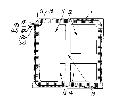
With reference to Fig. l a plane view of a gate matrix 1, or
an integrated circuit, is illustrated. This circuit
.<
comprises a base-bar 20 and thereto applied metal layers,
intended to form required connecting conductors between the
NMOS and PMOS transistors, resistances, etc., formed within
the base-bar. The base-bar 20 is formed so that during the
manufacturing process a gate sea 10 is formed with a central
position.
Other functional units 11, 12, 13, 14, such as memory units,
calculating circuits, processors and likewise, can also be
positioned within or around the gate sea 10, but these parts
are not further described since they are not an essential
part of the present invention.
A gate matrix l, according to the embodiment illustrated in
Fig. l,.is equipped with a large number of edge related
connecting surfaces or pads (bond-pads), where one of these,
given a position at the top left edge, has been numbered 15.
' -.:
This bond-pad 15 is a partvof an edge-related circuit 16:
The circuit 16 is a control voltage generating circuit made
out of NMOS transistors and/or likewise, which is
illustrated in Fig. 3.
The circuit 16 only has one connecting surface for an
external connection, cahich is the bond-pad 15, and this is
intended to connect to a selected reference resistance. The
reference resistance is connected with one connection to the
bond-pad 15, and the other connection is connected to a
circuit external ground potential or likewise {not
illustrated).
WO 95/26076 ~ ~ PGT/SE95/00279
- 13 -
Next to the circuit 16 there are one or several I/O
circuits, where a first of these has been given the number
17.
Each and every one of the I/O circuits 17 can have one or
two bond-pads 17a,~17b for a signal receiving circuit and
for a signal transmitting circuit, intended to connect
..,
external conductors (Ll, L2).
The I/O circuit 17 presents two external bond-pads 17a, 17b
intended to coact with one conductor each (Ll, L2) for the
information-carrying signals and a "differential" signal
transmission.
Each and every such I/O circuit can be equipped with
required bond-pads (~17a, 17b) for incoming information-
carrying signals and required bond-pads .or outgoing
information-carrying signals.
These bond-pads will not be described in more~detail since
the number of, and the positions of, these bend-pads, and
-..~,~:
the distribution of the bond=pads, is not a part of the
present invention.
The basis of the invention is that an input-circuit, a ~ v.
signal receiving circuit, is to be provided with various
selected resistance values as terminating impedances.
The edge-related surface area belonging to the circuit 17
and the input circuit requires hereby the access of an
adjacent surface area 18, where the terminating impedance,
according to Fig. 5, and the circuit 60 can be formed, which
will be described in more detail in the following.
Fig. 2 illustrates a cross section of a gate matrix 1
comprising a base-bar 20 where, in a known way, a number of
~~VO 95126076 ~ ~ ~ PCTISE95/00279
- 14 -
NMOS transistors, PMOS transistors, and other connecting
elements required in a "standardized" or custom-designed '
gate matrix are formed.
On top of the base-bar 20 there is a first metal layer 21
and a first isolating layer 22, a second metal layer 23 and
a second isolating layer 24, and yet a.third metal layer 25.
The metal layer 21 is~mainly intended to form the required
connecting conductors between the used PMOS and/or NMOS
transistors in the base-bar 20 in order to create a
predetermined connection of these transistors.
The isolating layer 22 is intended to separate these
conductors from the second metal layer 23 that mainly is
ntended to .supply power to selected points of meta?_ lay ar
21.
The NMOS and PMOS transistors and required~connecting
conductors used by the circuit 16, intended among other
things for a used differential operational ainglifier, are
thus supplied by the base-=bar 20 of the gate matrix 1 and
the mechanical and electrical connections are mainly done
through the metal layer 21 but also through the metal layer 'r'
r: iy.
23. a
With this background the present invention will now be
illustrated.
The indicated circuit 16, according to Fig. 3, is thus
intended both to provide a resistance value, serving as a
reference, made out of a parallel connection of an external
reference resistance 35, connected between a bond-pad 16 and
ground potential, and an internal adjustable resistance 37,
and to provide an adjustable control voltage, or
insignificantly variable control voltage, that is to control
WO 95/26076 PGT/SE95/00279
2~ss~oo
- 15 -
the momentary resistance value of an input impedance or
input resistance belonging to a signal receiving circuit 40
within a signal receiving unit in the I/O circuit 17.
The control voltage is thus adjustable to provide the
resistive component of the input impedance with a value that
is appropriate for signalling matching. The control voltage
can thereby be considered as constant over short periods of
time and variable over longer periods of time to be able'to
compensate for slow trends, such as temperature variations.
The basis of the function of the circuit is that minor
variations of the control voltage insignificantly influence
variations of the resistance value of the matching circuit
that presents resistive properties and belongs to the signal
rYCeiving circ:ui.t.
A circuit 31 for generating a control voltage on conductor
30 comprises, according to Fig. 3, a differential
operational amplifier 32 having two input terminals 32a, 32b
and one output terminal 32c. ~v'
The circuit 31 comprises also two current circuits 33, 34
(which can be resistances) serving as current generators, -:..
- >':
where one of these circuits 33 conducts.a current through a '~E
resistance 35, and preferably the circuit is externally
connected and serves as a reference, to-ground potential 36.
The voltage "U1" that appears across the resistance 35 is
connected to one input 32a of the two input terminals of the
operational amplifier 32.
The other circuit 34 of the two current circuits conducts a
current through an NMOS transistor 37 to ground potential,
and the voltage "U2" that appears across the drain and
source terminals of the NMOS transistor is connected to the
WO 95/26076 21 g 610 0 p~/SE95I00279
- 16 -
other input terminal 32b.
The control voltage appears on the output terminal 32c of
the operational amplifier 32 and is connected, via a
conductor 37a, to~the gate terminal 37g of the NMOS .
transistor 37.
Fig. 4 is intended to illustrate a signal receiving unit 40,
' belonging to an I/O circuit 17, with a signal receiving
circuit (not shown) to which the conductors L1, L2 are
connectable, each of the conductors having one bond-pad 17a,
17b. Voltage variations, representing a digital
information-carrying signal, appear on the conductors, and
the conductors are both connected to a terminating load 41,
in the form of one NMOS transistor each 42, 43.
It should be noticed that in the embodiment illustrated in
Fig..4, the received information-carrying voltage pulses or
voltage variations can be of a very low frequency and
exhibit good quality reception and signal.processing.
''
An increase of the frequency up to the,'kilohertz (kHz) range
does not present any problems with required reception and
signal processing.
With a circuit according to the present~invention, however,
in a practical application, voltage pulses appear on the
conductors L1, L2 with a frequency_from the megahertz (MHz)
range up to the gigahertz (GHz) range, as the invention is .
applied according to a "differential" or "single-ended"
signalling system.
If a "single-ended" signalling system is used, one of the
conductors, say L2, is connected to a reference voltage or
simply just disconnected, and the NMOS transistor 43 can be
omitted.
WO 95/26076 pCT/SE95/00279
- .-
- 17 -
Fig. 4 illustrates the possibility to not only connect the
control voltage 30' to the terminating load 41 of-:the I/O
' circuit 17 but also to the terminating lbad 4la of an
adjacent I/O circuit, and so on, to further terminating
loads, the further terminating loads not shown but
indicated.
These parallel-connected terminating loads can thus belong
to remaining I/O circuits belonging to the shown gate~matrix
1.
The generated and adjusted control voltage on conductor 30
.also apgears on the conductor 30', and the adjusted
resistance value of the NMOS transistor 37, in parallel with
i5 the reference resistance 35, corresponds to a resistance
- value of the NMOS transistors 42, 43'; which is controlled by
the control voltage 30.
The resistance values of the NMOS transistors 42, 43 can
thus be regarded as replicas of the adjusted resistance
value within the circuit 16.
-~-~,.-
If the resistance values of the NMOS transistors 42, 43,
with a generated control voltage and a selected value of the
reference resistance 35, do not match the transmission media
(conductors L1, L2), then it is possible to achieve such a
match by changing the value of the reference resistance 35.
' The ground potential or zero potential or selected
terminating voltage 36 (VT) of the circuit 31 is to be the
same as the corresponding potential of the circuit 41.
A connecting arrangement according to the present invention
can thus, in Fig. 3, replace the shown transistor 37 or, as
exemplified in the following description and illustrated in
Fig. 4, replace the shown transistor 42 and/or the
WO 95/26076 PGT/SE95/00279
- 18 -
transistor 43. A connecting arrangement according to the
present invention can also make use of the resistance "R1"
according to the illustration in Fig. 4.-
The connecting arrangement according to Fig. 5 comprises a
number of NMOS transistors, oriented in a row "N", where
each and~every gate terminal of the transistors points to
the left while the drain and source terminals of the
transistors point to the right.
The latter are, according to the pattern illustrated in .
Fig. 5, connected to a conductor "0" presenting a voltage
reference (VT), normally in the form of a ground reference,
a signal conductor "L1", or a signal conductor "L2".
The voltage reference (VT)-or terminating voltage can, as
illustrated, be zero-potential and/or ground potential, but
it can also be another, negative or positive, potential.
To simplify the following description it is'~assumed that the
reference potential is zero-potential. .~i:;.._
The NMOS transistors in Fig. 5 have been numbered NT50 to
NT74 next to the gate terminal of each respective
s, ,
transistor.
To be operated, the invention uses at least one analog
control signal that is connected to one or several control
connections numbered 51, 52, 53, 54.
Every control connection is connected to the-,gate terminals
of a group of NMOS transistors, and the drain and source
terminals of the transistors are connected to the
conductors L1, L2, and "0" respectively. The control
signal, in the form of a control voltage, and the remaining
parameters of the used transistors are selected to be
.4.
WO 95126076
PGT/SE95/00279
- 19 -
within; or at least close to, the resistive region of the
drain-source section of the transistors.
.< ,
Fig. 5 illustrates thus that a first control connection 51
coacts with a first group of transistors, where the group
NT54, NT55 is connected between the voltage reference
conductor "0" and the conductor L1, and the group NT51, NT58
. is connected between the conductor "0" and the conductor L2.
A second control connection 52 coacts with a second group of
transistors, grouped one by one, and numbered NT50, NT52.
A third control connection 53 coacts with a third group of
transistors, which is a series connection of the transistors
NT56, NT57; NT60, NT61; NT64, NT65; and NT68, NT69, where
the pair-wise transistors NT64, NT65 and NT60.,..NT61 (.and
NT53) are deactivated since the drain and source terminals
are connected to the conductor "0".
A fourth control connection 54 finally indicated by Fig. 5
coacts with a fourth group of transistors NT~2_ NT63, NT66,
NT67; and NT70, NT71, NT72~,~NT73.
The transistor NT74 is illustrated~as disconnected.
~...:1
The number of transistors within a first group, such as the
group related to the connection 5I, is different from the
number of transistors within a second group, such as the
~ group related to the connection 52. The same applies also to
the transistors related to connections 53 and 54.
The embodiment shown in Fig. 5 indicates that the number of
NMOS transistors can be chosen to be between ~ and 4
transistors.
WO 95/26076
PCT/SE95/00279
- 20 -
By ~ transistor is meant a series connection of two
transistors, and.by:.2, 3, or 4.transistors is meant a
parallel connection of two, three, or._four transistors.
It is evident that the number and configuration of the used
group-related transistors provide a specific resistance
value depending on the selected voltage value of the
connections 51, 52, 53, 54.
The conductors constitute signalling conductors where
digital information in the form of voltage pulses is
transferred.
To be able to create conditions for a signal receiving
circuit to evaluate voltage pulses with a high rate, for
..instance more than.200.Mb/s, a well-matched impedance.is
required; depending on the parameter variations of the so
called terminating resistances.
The circuit, according to the invention and:~~Figs. 5 and 6,
can advantageously be connected as a terminating impedance
in a signal receiving unit.
The circuit 50 can be used with "sirigleTended" signalling,
with one of the conductors (L1 or L2.) connected to a fixed
reference voltage or simply disconnected, or with
"differential" signalling according to the illustrated
wiring diagram in Fig. 5.
The required control signals, appearing as voltage values on
connections 51, 52, 53, 54, are adjusted with connecting
.;
means 60 illustrated in Fig. 6.
The connecting means 60 comprises a number of analog
transmission gates 61, 62, 63, 64, each made out of one NMOS
WO 95/26076 ~ PCT/SE95J00279
- 21 -
transistor and one PMOS transistor connected to each other
in parallel.
Each and every one of these analog transmission gates 61-64
can be activated or deactivated by a signal inverting
circuit 65 comprising one NMOS transistor and one PMOS
transistor connected to each other in series.
A high signal on conductor 66 to the inverting circuit 65
disconnects all the analog transmission gates 61-64, and a
' low signal on conductor 66 connects the analog transmission
gates 61-64.
The potential of the signal connections 51-54 is connected
to the potential of the "0" conductor through the
_ transistors 61a;. 6.2a; 63a, 64a upon disconnection of.fihe
transmission gates.
An analog transmission gate 61 coasts with a first control
connection 51 related to a first group of transistors; a
second analog transmission gate 62 coasts with a second
. control connection 52 related to a second group of
transistors; and so on.
The control voltage belonging to the~analog transmission r:'
gate 6l~and appearing on the conductor 67 can be given a
digitized voltage value, which will result in the
transistors NT54, NT55; NT51, NT58 presenting a previously
determined resistance value.
If the control voltage belonging to the analog transmission
gate 61 is given analog voltage values, then the transistors
NT54, NT55; NT51, NT58 will present a resistance value
corresponding to the voltage value on,~the conductor 67.
v.
WO 95/26076 PCTlSE95/00279
_ 2~8~~.00
- 22 -
These conditions apply also to the analog transmission gate
62 with conductor 68, the transmission gate 63 with
conductor 69, and the transmission gate 64 with
conductor 70.
The exemplified embodiment illustrates that the voltage
value appearing on conductor 30' corresponds to a selected
terminating reference generated by the circuit 16
illustrated in Fig. 3.
it is obvious that digital or analog control voltages can be
connected to any of the transmission gates depending onset
requirements and provided possibilities.
The voltage variations on conductor 30' can thus be
connected to one or several of the conductors 67-70.
It can be advantageous to connect the voltage variations on
conductor 30' to one or several of the conductors 67-70
depending on used supply voltage, or other parameters, in
order to thereby create a terminating resistance that is
adjustable to the present~conditions, such asr.temperature,
process parameters, supply voltage, etc:_
The circuit 50 requires a macro area~of.its own, preferably
immediately adjacent to the macro area of the signal
receiving unit or the macro area of the circuit 16.
The number of transistors, or the gate-width, can be
selected so that the control voltage can be as high as
possible, but still within the present supply,_voltage and
output voltage of the amplifier.
Tf the voltage VDS would be so high that the drain-source
section of the transistors no longer presents resistive
WO 95126076 PCTISE95/00279
21$6100
- 23 -
properties, then the transistors would operate as current
generators.
.< ,
Fig: 8 illustrates a voltage/time diagram at various
selected resistance values provided by the transistor
connections according to Fig. 5.
The following resistance values have been used during the
time intervals A - P. ~ w
4x 2x x x/2 "R"
(54) (51) (52) (53) [ohm]
A 0 0 0 0 0,0
B 0 0 0 1 0, 5
C 0 0 1 0 1~0
D 0 0 1 1 1, 5
E 0 1 0 0 2, 0
F 0 1 0 1 2, 5
G 0 1 1 '_- ~0 3 , 0
H 0 i - . 1 ~ i 1!"'~ 3 , 5
I 1 0 0 0 4, 0
J 1 0 0 1 4, 5
K 1 0 1 0 5 , 0 ~;
L 1 0 1 1 5, 5.
M 1 1 0 0 6, 0
N 1 1 0 1 6, 5
O 1 1 1 0 7, 0
P 1 1 1 1 7, 5
This digital connection ence, wherethe digital value
sequ
"1" is intended representone of many values,
to available
illustrates how number nd dimensioning
the a of the
transistors within availablegroups are selected be tween the
groups so connection as described above of
that a sequential
WO 95/26076 PCT/SE95/00279
~~.86~U~
- 24 -
indicated-groups will be able to provide a series of
resistance values in steps of 0,5 ohm..
This.is performed with a resistance variation weighted in a
unanimous way-according to a digital series. .
It is possible to select a resistance value from a
continuous resistance variation by selecting and applying an
analog control voltage to one or several of the connections
51-54.
If a voltage of 0,25 V is desired, this can be achieved by
selecting the resistance values of the time interval E or F
or, alternatively, selecting an adjusted resistance value
between these two. ,
it is evident that an arrangement according to the invention
can be adapted to be used as a terminating impedance related
to a signal transmitting unit, or any other device that
reguires a matching impedance, as well as a_signal receiving
unit, even though the exemplifying embodiment in this
description have described the arrangement related to a
signal receiving unit.
It will be understood that the invention is not restricted
to the aforesaid and illustrated exemplifying embodiments
thereof and that modifications can be made within the scope
of the following claims.