Note: Descriptions are shown in the official language in which they were submitted.
CA 02186104 1999-03-18
SIGNAL RECEIVING AND SIGNAL PROCESSING UNIT
The present invention relates to a signal receiving and signal
processing unit. The invention relates more specifically to a
signal receiving circuit and a signal processing circuit where
the character of the signals are in the form of pulse-shaped
voltage variations having a selected high repetition
frequency, such as from the megabit per second (Mb/s) area up
to the gigabit per second (Gb/s) area, more than 1 Mb/s and
preferably more than 100 Mb/s.
The voltage variations are controlled to represent a digital
information-carrying signal, with an internal structure, by a
transmitting circuit. The digital signal is distorted by,
among other things, the signal transferring conductor. The
receiving circuit is intended to be able to detect and receive
a thus distorted digital signal.
Units of this kind are used to adapt received (distorted)
signals into transmitted signals having an internal signal
structure. A received signal which presents a somewhat
erroneous voltage level and/or is not adapted to a certain
common mode (CM) area is to be adapted, by the signal
processing unit, to an internal signal structure more suitable
to the requirements that are needed in an exchange of signals.
3Q Such signal receiving and signal processing units are
connected to a conductor adapted to transmit information-
carrying signals in the form of voltage pulses. The conductor
is connected to a transistor, belonging to a signal receiving
circuit, to have an effect upon a current by using variations
in the voltage pulses and the voltage value of a pulse. The
current is in the form of pulses that are passing through the
transistor, and the current is generated by voltage pulse
variations and a voltage level. In the signal processing
CA 02186104 1999-03-18
- 2 -
circuit, the current is adapted to an information-carrying
form better suited to the internal circuit structure than the
received signal was.
Signal receiving and signal processing units of this kind have
been useful to evaluate the information content in voltage
pulses having pulse rates in the range of up to 200 Mb/s.
Signal receiving and signal processing units of this kind have
been adapted to be able to detect pulse-shaped voltage
variations appearing on a single conductor (single-ended
signalling), or appearing on or between t~~ro conductors
(differential signalling).
The follocaing description will, in the interest of simplicity,
be limited to the application where differential signalling is
used, even though the invention is applicable to both types or
signalling systems.
It is obvious to one skilled in the art what measures are to
be taken to keep the voltage potential of one conductor at a
constant level, which is required at single ended signalling.
This will, nevertheless, be described in the following.
It is known to use various techniques to manufacture these
signal receiving and signal processing units to thereby
achieve various working conditions.
Both Complementary Metal Oxide Semiconductor (CMOS) technology
and bipolar technology have been used to manufacture signal
receiving units and signal processing units of the
aforementioned kind. The following description will mainly
describe CMOS technology, as the differences in function due to
the use of bipolar technology are of minor significance and are
obvious to one skilled in the art. It is further obvious to one
skilled in the art what changes are
WV yJILOUl2f PCT/SE95/00280
' _ ~~gs~o~
required to adapt CMOS technology and/or bipolar technology to
other known technologies.
When manufacturing units of this kind there are, among other
things, the following criteria that are of significant
importance.
A. The span and voltage values of the CM area
pertaining to the signal receiving circuit and
the signal processzii~ circuit.~'(The CM area is
the voltage area that the received voltage
pulses are to be within to be detected by the
signal receiving circuit, in a differential
transmitting system.)
B- The limiting value of the repetition frequency,
which is the highest frequency of the voltage
variations on the conductors that can be
detected and distinguished frcm each other by
the signal~~eceiving circuit and thereafter -
processed by the signal processing circuit.
C. The voltage variations or amplitude variations
that are required to detect the signals, where
small amplitudes can be accepted at low rates,
but at higher rates greater amplitudes are
required.
It is knocan to connect the information-carrying signals that
3'U appear on the conductors to the gate connections belonging to
PMOS transistors, cahere the CM area comprises the voltage area
from somewhat above half of the supply voltage (Vcc) docan to
zero potential_
The use of a PMOS transistor and a post-connected current
mirror or a post-connected cascode connection likecaise
provides a downward extending CM area, to somewhat below zero
potential (approximately -0.7 V).
CA 02186104 1999-03-18
- 4 -
It is also known that P-channel Metal Oxide Semiconductor
(PMOS) transistors present a lower limiting value of the
repetition frequency (up to 200 Mb/s) than that provided by
N-channel Metal Oxide Semiconductor (NMOS) transistors.
S
Using NMOS transistors instead of PMOS transistors caould
provide a CM area extending from the supply voltage down to
somewhat below half the supply voltage. This is not acceptable
since, in a practical application, the CM area has to be at
least within the area that is provided with PMOS transistors
and a post-connected current mirror or a cascode connection.
When constructing signal receiving and signal processing units
of aforementioned kind, it is known to use and coordinate two
transistors within the signal processing circuit so that a
current passing through a first transistor is mirrored to be
the same through a second transistor, and the drain-source
voltage of the second transistor can be permitted to vary
relatively greatly in relation to the current variation
through the first transistor.
It is also previously known to make the current through the
second transistor further independent of the drain-source
voltage (a high impedance current generator) by means of a
cascode connection. Other current mirror connections are also
known, such as a connection having three transistors known as
the "Wilson Current Mirror".
3O
CMOS technology uses PMOS transistors and NMOS transistors,
and in the following, transistors will be described with an
"N" or a "P" before their reference numerals to indicate
whether the transistor is an NMOS or a PMOS transistor,
respectively.
CA 02186104 1999-03-18
- 5 -
The expression "current mirror" will in the following
description and claims be understood to cover every kind of
current mirror regardless of whether two, three, or more
transistors are used. The Wilson circuit and the cascode
circuit represent current mirror connections that provide
better attributes when connected as current generators.
While the following description uses the term "NMOS
transistors", this term should be considered to include
bipolar NPN transistors and equivalent transistors of other
technologies. Bipolar PNP transistors and the like are also to
be included in the term "PMOS transistors".
It is further known that selected current values through a
signal receiving transistor are, within a certain area, in
direct proportion to the ability to receive, detect, and
process signals of a higher rate.
The upper Limit of the current value is set to where the
transistor leaves or goes out of the amplifying mode because
of the current density within the transistor.
The present invention can be regarded as a further
development of the signal receiving and signal processing
unit that is described in more detail in Canadian Patent
Application 2,182,943 filed February 16, 1995 by the
present inventor.
Considering the prior art, as described above, and with
respect to the trend within this technical field, it should be
regarded as a technical problem to be able to present a signal
receiving unit where the transistor or transistors belonging
to the signal receiving circuit are supplied through a
specific current generating circuit where the value of the
current through the transistor is adjustable in order to be
WO 95/26078 PCT/SE95/00280
2.~8~104
- 6 -
able to change the maximum rate so that the signal receiving
circuit has the ability to receive, detect, and process at a
higher transfer rate.
It must also be regarded as a technical problem to be able to
create'conditions where a selected current value is selectable
in several steps so that one of several fixed current values
can be selected along with one of several available maximum
transfer rates.
It is also a technical problem that when the current values
are adjustable in steps, each and every one of these steps
should be formed through the activation of one or several
devices belonging to a current generating circuit, where every
device is generating a partial current.
There is a technical problem in being able to indicate such
.k_
construction details so that the partial-current generating
devices can be activated and deactivated by means of a control
circuit in order to gene~~ate digital and/or analog signals.
There is also a technical problem to be able to indicate that
respective partial-current generating device is to be
activated and deactivated by means of a controlled transistor
where the voltage value of the gate terminal of a control
transistor is determined by the state of two series-connected
transistors, one being a PMOS transistor and the other being
?.
an NMOS transistor, where the;~gate terminals of the series-
connected transistors should be mutually connected and
affected by the output signal of the control circuit.
Zt should also be regarded as a technical problem to be able
to indicate a current-generating circuit which besides this is
able to provide an analog adjustment of the current value.
It is a further technical problem to be able to realise~.the
technical connecting measures that are required so that the
CA 02186104 1999-03-18
- 7 _
current generating circuit can be connected or disconnected
through a voltage pulse appearing on a conductor.
With the intention of solving one or more of the aforesaid
technical problems, the present invention relates to a signal
receiving and signal processing unit connected to at least one
conductor adapted to transmit information-carrying signals in
the form of voltage pulses. The unit comprises
a signal-receiving circuit including a transistor connected to
the conductor to have an effect upon a current by using
variations in the voltage pulses and a voltage value of a pulse,
where the current is in the form of pulses that are passing
through the transistor and the current is generated by the
voltage-pulse variations and a voltage level. A signal-
processing circuit adapts the current to information carrying
form. The transistor is connected with at least one other
transistor to form a current mirror, and the ability of the
signal-receiving circuit to receive, detect, and process the
signals is adjustable through a current-generating circuit in a
way so that an increasing current value provides a detection of
a voltage pulse at an increased rate and vice versa.
In one embodiment, the current values are adjustable in steps
that are formed by the activation of one or several devices
belonging to a current-generating circuit, where every device
is generating a partial current.
The partial-current generating devices are activated and
deactivated by a control circuit that can be activated by
digital signals.
Partial-current generating devices are activated and
deactivated by a controlled transistor. The voltage value of
the gate terminal of the control transistor is determined by
the state of two series-connected transistors, one being a
PMOS transistor and the other being an NMOS transistor, where
the gate terminals of the series-connected transistors are
CA 02186104 1999-03-18
_ g _
mutually connected and affected by a digital output signal of
the control circuit.
According to another embodiment of the present invention,
the current can be adjusted in an analog way to select a
maximum rate from a continuous rate scale of the signal to
detect and process the information-carrying signals. The
current-generating circuit can be connected or disconnected
through a logical signal, such as a voltage pulse,
appearing on a conductor.
The advantages primarily afforded by an inventive signal
receiving and signal processing unit, according to the present
invention, is that hereby has the possibilities to adjust the
ability of the signal receiving circuit to receive, detect,
and process signals been provided by means of an adapted
current value. The current is adjustable such that an
increasing current value provides an increased maximum
transfer rate, and the signal receiving and signal processing
can be performed with a high separation ability, and vice
versa.
Preferred embodiments of a signal receiving and signal
processing unit in accordance with the present invention will
nova be described in more detail with reference to the
accompanying drawings, in which:
CA 02186104 1999-03-18
- 9 -
Figure 1 illustrates a general block diagram of a unit
according to the invention;
Figure 2 illustrates a cairing diagram of a signal
receiving and signal processing unit; and
Figure 3 illustrates a wiring diagram of a current
generating circuit.
A unit according to the invention is illustrated by the block
diagram in Figure 1, which shows a signal receiving and signal
processing unit 1 and a current-generating circuit 10. The
current-generating circuit 10 can be affected by a control
circuit 100 in order to generate one of several available
fixed current values.
The circuit l0 is also able-to generate a current value
according to an analog voltage value through the control
circuit 100.
A current value that has been selected in an analog cvay can be
added to one or several of the fixed current values.
Reference may be made to the description of the
aforementioned Canadian Patent Application for a more
detailed understanding of the signal receiving and signal
processing unit 1, according to Figures 1 and 2.
3g
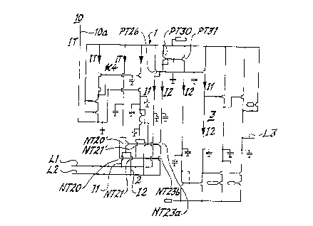
The signal receiving and signal processing unit 1 is thus
connected to one or several conductors L1, L2, respectively
adapted to transmit information-carrying signals in the form
of voltage pulses. The conductor L1 is connected to a
transistor NT20 belonging to a signal receiving circuit 2. A
WO 95/26078 PCT/SE95100280
- 10 -
transistor NT21 is provided for the conductor L2.
The variations in the voltage pulses on the conductors L1, L2
and the voltage value of a pulse have an effect upon both a
pulse-shaped current 11 passing through the transistor NT20
and a pulse-shaped current 12 passing through the transistor
NT21. A signal processing circuit 3 adapts a current signal
into an information-carrying form on the conductor L3.
The transistor NT21 belonging-to the signal receiving circuit
2 is coordinated with at least one other transistor NT23b to
mutually form a current mirror. The total current IT passing
through each transistor is adjustable through the current-
generating circuit 10 connected to the conductor 10a. The
ability of the signal receiving circuit to receive, detect,
and process the signals is thus adjustable such that an
increasing current value provides an improved and increased
sensitivity, improving the reliability of reception and
increasing the rate of processing, and vice versa.
The total current value IT is adjustable in steps where each
and every step is formed by the activation of one or several
devices 11, 12, 13 belonging to the current-generating circuit
10 in Figure 3. The devices 11, 12, 13 each generate a partial
current.
The partial-current generating devices 11, 12, 13 are
activated and deactivated by ~~oltage pulses that appear on
conductors 16a, 17a, respectively. The voltage pulses are
activated by control circuits 15, 15a.
A conductor 16a belonging to the control circuit 15 is
connected to the first and third partial-current generating
devices 11, 13, while a conductor 17a belonging to the control
circuit 15a is connected to the second and third partial-
current generating devices 12, 13.
WO 95/26078 PCT/SE95/00280
- 11 -
A low signal is generated on the outgoing conductors 16a or
17a in response to a high signal from the control circuit 100
on conductor 16 or 17.
A control circuit 100 is arranged to select and activate the
signals appearing on the conductors 16,17, 21, in order to
thereby select a current value or combination of current
values corresponding to a desired highest bit rate.
The control circuit 100'can also generate an analog signal on
the~conductor 20 to activate or deactivate the devices 1'l, 12,
13 or 14.
Only the device 11 is described below since the illustrated
partial-current generating devices lI, 12, 13 in Figure 3 are
substantially the same. The first partial-current generating
device 11 can be activated to supply a current and deactivated
Y
Z~
by means of a controlled Nt~iOS transistor lla_ The voltage
value of the gate terminal of the control transistor is
determined by the state of two series-connected transistors,
one being a PMOS transistor and the other being an NMOS
transistor. The gate terminals of the series-connected
transistors are mutually connected and affected by the output
signal of the control circuit 100 and a signal that is
connected through the control circuit on the conductor 16a.
A low logical level appears on.conductor 16a if there is a
high logical level on conductci- 16, and the device 11 is only
activated if there simultaneously appears a low logical value
on the conductor 17.
The second device 12 is activated if a tom logical value
appears on conductor 16 and a high logical value appears on
conductor I7.
Not only the two devices 11 and 12 but also the third device
13 is activated at a high logical level on conductor 16 and
conductor 17.
1'1 V 7J/GUV /O
PCT7J~ysIUU2liU
- 12 -
A previously determined current value through the device 11 is
determined by the value of the transistor llb; the current
value through the device 12 is determined by the value of the
transistor 12b; and so on.
One of several available fixed current values (0; I11; I12;
and I11 + I12 + I13) can be selected through the circuit 10 at
the dimensioning of the devices 11, 12, 13.
An addition can be made to, each andwevery one-of-these current
values by a further analog~current value, I14 which is
proportional to the value of the voltage appearing on
conductor 21. This is useful for increasing the current value
above the fixed values that are provided by the devices 11,
12, and/or 13.
All devices 11, 12, 13 can be connected or disconnected
through a high or lo;a logical value, generated by the control
w circuit i00, on a conductcr 2Q.
The current "Iref" is cut off by the transistor connection
T30, and the conductor 32 is connected to the reference
voltage (zero level) on conductor 33 through a transistor T31.
The devices 11, 12, 13, 14 a-re blocked at a high level or
voltage on conductor 20.
The current value to the signal receiving circuit can be
adjusted in an analog way using an adjustable voltage value on
the conductor 21, even when the devices 11, 12, 13 are
3~ ._-rlisconnected, by activating the transistor 14a (activated by a.
cascode reference voltage) within the circuit 14 and
permitting the transistor 21a to adjust the current value
according to the current voltage value on the conductor 21.
The current value IT can be selected to be much higher then
"Iref" through the dimensioning of the transistor llb by using
a number of transistors connected in parallel.
WO 95/26078 PCT/SE95I00280
- 13 -
It will be understood that the invention is not restricted to
the illustrated exemplifying embodiments thereof and that
modifications can be made within the scope of the following
claims.
~x-
l: