Note: Descriptions are shown in the official language in which they were submitted.
W096/26523 2 1 8 6 1 4 1 PCT~S9~02258
AN ITERATIVE METHOD OF RECORDING ANALOG SIGNALS
BACKGROUND OF THE INVENTION
1. Field of the Invention:
The present invention relates to the field of non-
volatile integrated circuit analog signal recording and
playback devices wherein an analog signal is directly
stored in and read back from a storage cell.
2. Prior Art:
Application serial number 07/588,949 discloses a
high density integrated circuit, analog signal recording
and playback system wherein an analog input signal is
sampled a plurality of times and then, as additional
samples are being taken and temporarily held, a prior
set of samples of the analog signal are simultaneously
loaded into an equal plurality of storage sites or
memory cells, preferably EEPROM cells. In that system
the read process and circuitry connects each
electrically alterable MOS storage device in a source
follower configuration, which provides a one-to-one
relationship between the variation of the floating gate
storage charge (voltage) and the variation in the output
voltage, with an insensitivity to load characteristics.
That system's write process and circuitry provides a
multi iterative programming technique wherein a series
of coarse pulses program a cell to the approximate
desired value, with a series of fine pulses referenced
to the last coarse pulse being used for programming the
W096126523 2 1 ~ 6 1 4 1 -2- PCT~S95/02258
respective cell in fine increments to a desired final
programming level. The iterative write process is also
disclosed in detail in application serial number
07/636,879, with products generally in accordance with
these disclosures being sold by Information Storage
Devices, the assignee of the present invention, as its
ISD1016 devices.
BRIEF SUMMARY OF THE INVENTION
Method and apparatus for adjustment and control of
an iterative method of recording analog signals with on-
chip trimming techniques for later playback. The
invention allows setting of various parameters for the
multi iterative programming technique after chip
fabrication so as to allow tighter control and thus
higher resolution analog signal sample storage in a
given or minimum amount of time. Such parameters
include, but are not limited to:
1) the step down voltage from the coarse
programming cycle to the fine programming cycle.
This is required to ensure that the first fine
pulses do not cause programming, i.e. add charge
increments to the floating gate cells which are
greater than the expected amount for each fine
pulse in the center of the fine programming cycle
when it has reached equilibrium. In particular,
each fine pulse in the center of the cycle causes
essentially an equal amount of charge increment to
the floating gate of the EEPROM cell.
2) the incremental voltage increase between
each fine pulse.
W096/26523 2 1 ~ 6 1 4 1 PcT~s95lo225g
--3--
3) the pulse width of each fine pulse.
4) the number of fine pulses.
5) the incremental voltage increase between
each coarse pulse.
6) the pulse width of each coarse pulse.
7) the number of coarse pulses.
8) the offset, VOS, which stops further coarse
pulses and holds the last coarse level as a
reference for the following fine cycle.
BRIEF DESCRIPTION OF THE DRAWINGS
Figure 1 is a schematic circuit diagram of a part of
a-memory array and associated circuitry of an analog
storage device in accordance with the present invention.
Figure 2 is a schematic block diagram of a part of a
memory array and associated circuitry of an analog storage
device in accordance with an alternate and preferred
embodiment of the present invention.
Figure 3 is a detailed schematic diagram for the
diagram of Figure 2.
Figure 4 shows a block diagram of typical EEPROM
cells controlling blocks which adjust the multi
iterative programming technique parameters.
2186141
W096/26523 PCT~S95/02258
--4--
Figure 5 illustrates the prior art wherein the
voltage FV was switched from 2v to 0v at the beginning
of the fine cycle and then charged back to a 2v level by
the end of the fine cycle.
Figure 6 is a circuit diagram showing a fixed
voltage (FVSTEP) as applied to a switch SW2, which
switch is closed during the coarse cycle and passes
FVSTEP to FV which drives the bottom plate of C1 in
Figure 3.
Figure 7 is a circuit diagram showing the circuit
to control the value of FVSTEP.
Figure 8 is a circuit diagram showing the circuit
which drives the signal FVRCTL.
Figure 9 is a circuit diagram showing the circuit
that may be altered to adjust the incremental voltage
increase between each coarse pulse.
Figure 10 is a circuit diagram showing the circuit
for generating the signal VOS.
DETAILED DESCRIPTION OF THE INVENTION
The preferred embodiment of the present invention
represents a substantial improvement in the methods and
apparatus for iterative writing a signal sample to an
MOS storage cell for integrated circuit analog recording
and subsequent playback disclosed in copending U.S.
Patent application serial number 07/636,879, filed
January 2, 1991. To provide a basis for understanding
the nature of the improvement and the environment in
W096/26523 2 1 ~ 6 1 4 1 PCT~S95/02258
which the preferred embodiment is intended to operate, a
substantial part of the disclosure of that earlier
- application is repeated herein.
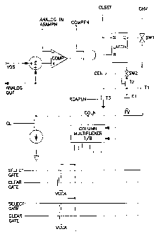
First referring to Figure 1, a basic implementation
of that invention may be seen. This figure represents a
section of a typical memory array with one column driver
consisting of comparator COMP, latch, high voltage (HV)
switch and column load, column multiplexer comprising
switches CMl to CMm and a memory array consisting of n rows
and m columns of transistor pairs Snm and Fnm. This figure
of course is representative of one specific embodiment as,
for example, there may be more than one column driver
multiplexed (or not multiplexed) into the array, there may
be more than one level of multiplexing of each column
driver into the array, etc. Also the figure shows a single
common node VCCA, but it may equally be separated into
different nodes. For the purposes of the description of
the first embodiment of that invention, the high voltage
switch is shown as a simple switch, though in another
embodiment disclosed herein the same consists of two
switches, together with means to superimpose a fine
adjustment voltage on a coarse voltage to more accurately
program the storage cell within the typical available time
for doing so.
A recording is made by the following sequence. The
cells to be written (programmed) are first erased
(cleared). This is done by applying a high voltage to the
clear gate CGn while maintaining a low voltage on the drain
of the cell. In the circuits of that embodiment, each row
has an independent connection in order to facilitate the
clearing of each row independently without disturbing the
analog samples recorded in other parts of the memory. The
low drain voltage is achieved by applying a low voltage to
VCCA. Since the high voltage on the clear gate causes the
2 1 86 1 4 i
W096/26523 PCT~S95/02258
--6--
floating gate transistor to be in a conductive state, the
low voltage is transposed to the drain. It would also be
possible to apply the drain voltage through the column and
select gate.
The voltage to be written is applied to ANALOG IN, a
SET signal is applied to set the latch and turn on the HV
switch, CL is taken low, all CG lines are taken low, and
the desired column multiplex lines (CMm) and select gate
lines (SGn) are taken high. Unselected columns and rows
have their CM and SG lines low. The first high voltage
pulse is then applied to HV and via the CMm and SGn
transistors to the drain of the addressed cell. The level
on CMm and SGn must be sufficient to pass the desired level
onto the cell drain. In the preferred embodiment of that
invention, CM and SG are higher than HV so that HV, the
regulated signal, is connected onto the drain without any
loss of voltage. It would also be possible to regulate CM
and/or SG in order to pass the desired level onto the
drain. As HV is applied to the drain, VCCA is also brought
positive. In the preferred embodiment of that invention,
the VCCA level, at this point in the procedure, is about 7
volts- this being higher than the maximum level to which
the Fnm transistor would otherwise pull VCCA by follower
action. (Note that although CGn is at VSS, the capacitive
coupling onto the floating gate causes the transistor to
conduct even though it may be strongly cleared.) The
purpose is to ensure that the column voltage does not
become suppressed due to a current path to VCCA. Non-
Suppression of VCCA could also be achieved by allowing VCCA
to float, which may be satisfactory for VCCA nodes with
small capacitance values and high voltage sources with low
source impedance values. These values generally do not
occur in practice. Now that the cell is in this writing
condition, electron tunneling may occur from floating gate
to drain, resulting in a net increase in the positive
W096/26523 2 1 8 6 1 4 1 PCT/u~55~2ZS8
charge residing on the float gate. After a certain time
period HV (and VCCA) is brought low, in the preferred
~ embodiment, and the discharge rate is controlled to avoid
unnecessary perturbations onto other nodes.
The cell is now configured into the read mode. CL is
taken high (connecting the current load onto the column),
CMm and SGn remain high to keep the same cell addressed
(although not necessarily at the same high voltages as
before) and VCCA is taken to a positive voltage. Note that
this configuration is a reversal from digital memories
where the VCCA node would be grounded. The total
resistance of the Snm transistor and the column multiplex
transistor(s) should be small compared to the effective
resistance of the load. The clear gate CGn voltage is
taken to a fixed level which is chosen to optimize the
voltage storage range - in the case of the preferred
embodiment that invention both VCCA and CGn are connected
to 4V. The voltage which is now output on the column is
compared with ANALOG IN. EN is brought high and if ANALOG
OUT is greater than ANALOG IN, the output of the comparator
goes high and resets the latch. The HV switch is thus
opened and the subsequent HV pulses are not connected to
the cell. (Typically such high voltage pulses are of
successively increasing amplitude.) If, however, ANALOG
OUT is less than ANALOG IN, then the latch remains set and
the next HV pulse is applied to the cell and the cells
obtains another increment of tunnel current. The cell is
alternatively configured in write mode and then read mode
until a comparison is reached or a maximum number of cycles
has been reached.
To play back the recording, the circuit is configured
continuously into the read mode. The configuration and the
cell operating conditions are exactly the same as during
the write comparison and thus an accurate reproduction is
W096t26523 2 1 8 6 1 4 l PCT~S95/02258
achieved.
The resolution of analog recording is improved if the
voltage increment on the EEPROM floating gate resulting
from each high voltage iteration is as small as possible.
In the case of commercially available speech recording
devices, resolutions range from 6 bits to 16 bits of
equivalent digital resolution. The recording method
employed herein causes the voltage on the floating gate to
be incremented during each high voltage pulse. The
resolution achieved depends on the width of the high
voltage write pulses and also on the amount of voltage
increment between each successive pulse. Better resolution
(i.e. smaller voltage increments) is achieved with narrow
pulses and/or with smaller voltage increments of the high
voltage pulse. However, this means that to cover the same
range of floating gate voltages (i.e. the same dynamic
range), there must be an increased number of applied high
voltage pulses. In a given recording architecture there is
a certain amount of time available to perform the writing
of one row before beginning the write of the next row.
This limits the number of pulses which can be applied and
consequently limits the resolution which can be achieved.
If the high voltage pulses increase linearly over the
complete range, then each increment would give
approximately equal increments to the floating gate. The
first few pulses (which generally would follow an erase
cycle) would probably cause a larger increment than
subsequent pulses, but this is the major exception.
The technique used in the preferred circuit of
Figure 2 of that invention uses two bursts of voltage
pulses (the method could be extended to more bursts).
The first burst of pulses has monotonically increasing
voltage levels (beginning with a level which produces a
weakly programmed cell and ending with a level which
W096/26523 2 1 ~ 6 1 4 l PCT~S95/02258
produces a strongly programmed cell - i.e. from 8 volts
to 18 volts). These will be called the coarse pulses.
Coarse pulses are applied to the cell until the cell
reaches a point where an additional pulse would program
it to a level which is beyond the desired level. A
second burst of pulses is now applied which has a
reduced voltage increment between adjacent pulses.
These are termed the fine pulses. The voltage level of
the first pulse in the fine burst is related to the
level of the last coarse pulse applied to the cell. It
can be the same level, slightly higher or slightly
lower, but the important thing is that it is a function
of the last coarse pulse height. Fine pulses are
applied to the cell until the cell is programmed to the
desired level. The voltage level of the fine pulses may
also have monotonically increasing values, but the
voltage increment is much smaller than the increment
during the coarse cycle. The fine pulses may also be of
a narrower width than the coarse pulses.
In this scheme, the resolution of the floating gate
voltage is determined by the voltage increment attained
during the fine cycle. The voltage range, however, is
determined by the coarse cycle.
Consider an ideal situation where:
Vr = Dynamic voltage range.
Vc = Floating gate voltage increment during coarse
pulses
Vf = Floating gate voltage increment during fine
pulses
NC = Number of coarse pulses
Nf = Number of fine pulses
Then,
Nc = Vr/Vc
21 86141
W096126523 PCT~S95/02258
--10--
Nf = Vc/Vf
and
Ntotal = NC + Nf
If the circuit did not use this dual (or multi)
increment technique however, and the same resolution was
required, then the total number of pulses required to
cover the range would be:
Ntota1 = Vr/Vf = Vr/(Vc/Nf) = Nc*Nf
As an example, suppose we have a range of lV, a
coarse increment of O.lV and a fine increment of lOmV.
Using the dual increment technique a total of 20 high
voltages would be required versus 100 pulses with pulses
of uniformly increasing magnitude.
In practice, the number of pulses required is
greater than the ideal case because: 1) one must begin
the coarse high voltage pulses at a lower level and
continue past the ideal high level in order to account
for manufacturing tolerances which change the
relationship between the applied high voltage signals
and the resulting voltages on the floating gate (e.g.
variations in tunnel threshold). This is necessary when
using either technique. 2) there must be a sufficient
number of fine pulses to cover the complete voltage span
of a single coarse step. At the upper end this is a
similar problem to 1), but at the lower end it is due to
practicalities in circuits which are used to implement
the technique.
A block diagram of a circuit which utilizes a dual
increment (coarse/fine) technique is shown in Figure 2.
In addition to the components of Figure 1, there is an
extra switch SW2, transistors T1, T2 and T3, capacitor
WO96t26523 2 1 ~ 6 1 4 1PCT~US95/02258
C1 and a voltage summing junction. To initialize the
circuit, a pulse is applied to CLSET to set the latch,
CEN is set high to close SW2 and a pulse is applied to
RCAPEN to discharge C1. The burst of coarse pulses is
then applied to CHV and consequently is also applied to
the cell provided that the latch remains set and SW1 is
closed, as described previously. One important
difference with this implementation compared to the
basic circuit is that the connection of CHV to COLN is
through the transistor T1. T1 requires a voltage on its
gate which, in turn is provided by SW2 and T2. During
the time that the cell voltage is read and compared with
ANALOG IN, a voltage Vos is added to the voltage on
COLN. The value of Vos is equal to or slightly greater
than the floating gate voltage increment that results
from a single coarse pulse. Adding Vos before the
comparison is made with ANALOG IN ensures that the latch
is reset one coarse pulse earlier than would otherwise
occur. At this time, the latch is reset and the cell is
thus programmed to a level which is no more than one
coarse increment below the desired level. Also the gate
voltage on T1 which corresponds to the last coarse pulse
before comparison is stored on C1.
The latch is now set once more by applying a pulse
to CLSET, CEN is taken low to open SW2 and the second
burst of high voltage (fine) pulses are applied to CHV.
These pulses are all of maximum amplitude, but the
voltage which is transferred onto COLN through T1
depends on the stored level on C1 and the follower
action of T1. The stored level on C1 is modulated by
the signal FV, which in the preferred embodiment, is a
ramp which begins at a low level (VSS) at the beginning
of the fine cycle and rises to a higher level (2V) at
the end of the fine cycle. The magnitude of the high
voltage pulses which are connected to the cell during
W096/26523 PCT~S95/02258
-12-
the fine cycle is therefore dependent on the highest
value reached during the coarse cycle and with
increasing amplitudes as determined by FV. As with the
coarse cycle, after each high voltage pulse the cell
voltage is read and compared with ANALOG IN. During the
fine cycle, however, Vos is held at VSS and the cell
voltage is incremented in fine increments until a
comparison is made.
Figure 3 shows a detailed schematic of the circuit.
T2, T3, T4, T6, T8 together with C1 and C2 create an
offset canceled comparator; T5, T7, T9, T10, T11, T12,
T13 and T14 create an additional gain stage and latch;
T15, T16, T17, T18, T23 and C3 create a high voltage
switch; Tl9, T20, T21, T22, T24 and C4 create another
high voltage switch; C5 is a holding capacitor and T29
acts as a source follower.
The write sequence begins with an erase cycle. In
the following description it is assumed that the
addressed cell has already been fully erased. When
reading, the cell is configured in a source follower
mode as previously described. The signal VCL applies a
bias to T32 such that T30, T31, and T32 act as a load to
VSS. (T30 is included to increase the voltage breakdown
on the COLN node). This technique could also be
utilized if the cell were configured in the arrangement
which is more conventional to memory arrays, but an
inversion would be necessary (for instance between the
cell and COLN).
At the beginning of the write (programming) cycle,
a negative pulse is applied to CLSET and a positive
pulse is applied to RCAPEN. This sets the latch (HVEN
goes high) and discharges C5 to OV. VCOMP provides a
bias such that T4 and T5 act as high impedance load
W096/26S23 2 1 8 6 1 4 1 PCT~S9s/022s8
devices. Likewise, VCOLHV causs T18 and T22 to behave
as load devices, in this case to VSS. P/R is held low
and is only allowed to go high during playback. CEN is
initially held low. CL is low during write and high
during read. The voltage which is desired to be written
into the EEPROM cell is applied to ASAMPN. The first
high voltage pulse of the coarse cycle is applied to
CHV. It could typically be about 10V amplitude with a
finite rise time and pulse duration. Since HVEN is low,
T17 is off and the voltage on the gate of T23 rises as a
result of the CHV ramp on C3. Other capacitances on the
gate of T23 are small relative to C3 and consequently
there is very little capacitive or voltage division.
There is also the self bootstrap effect of T23 itself
and so the gate of T23 increases in voltage by an amount
almost equal to CHV. The starting voltage on T23 gate
was (VCC - Vt) or about 4V, so with Vt typically about
lV, the transistor T23 is turned fully on and CHV is
conducted onto C4. The components T15, T16, T17, and
T18, T23 and C3 operate like a high voltage switch
enabled by HVEN (other implementations of the switch are
possible). In a similar fashion, the other switch using
T24 also conducts and C5 is charged to (CHV - Vt) - the
Vt drop is due to T25. T29 now conducts and allows COLN
to rise to (CHV - Vt - Vtn). Vt is the enhancement
threshold (of T25), and Vtn is the threshold of native
transistor T29. It is assumed that the Vt of T28 is
less than or equal to T25. Hence the CHV pulse is
applied to COLN and subsequently to the cell with a
small amount of voltage drop due to thresholds. After
CHV is returned to its low level, the voltage read from
the cell is compared with ASAMPN. CCK and CCK are
inverse signalsi CCK is initially high and gates ASAMPN
on to Cl via T2. T6 is also driven by CCK and biases
the invertor T8/T4 in its linear region and cancels the
offset. T7 gate has the same voltage as (matched) T8
W096/26523 2 1 8 6 1 4 l PCT~S95/02258
-14-
and its source is at VSS, so the invertor T5, T7, T9 is
also in the linear region. CCK then goes low and CCK
goes high. The cell has since been configured in its
read mode and thus the cell voltage is coupled onto Cl.
The change in voltage on the LHS of Cl is coupled onto
the gate of T8. (It is important that CCK goes low
before CCK goes high in order to ensure that there is no
charge loss through T6). Simultaneously, a positive
going signal is applied to Vos (in the preferred
embodiment it is 1.5V, derived from analog signal
ground) and couples additional charge onto T8. The
value of capacitor C2 is chosen so as to couple charge
that is equivalent to a voltage slightly greater than
the voltage increment that results on the floating gate
during each coarse pulse. Since the invertor is in its
linear region, the change at the gate of T8 causes a
corresponding change in the drain of T8, multiplied by
the gain of the invertor. The size of T6 is kept small
so as to minimize the capacitive coupling from CCK to
the input of the invertor. The coupling can be reduced
further by connecting an equal capacitor to the gate of
T8 but within equal and opposite phase of signal. This
can be a "dummy" transistor similar to T6, or, as is
often done, it can be a P-channel transistor in parallel
with T6 and driven by an opposite signal. these steps
were not taken, however, because the offset introduced
here is a systematic offset which is equal in all
similar circuits, including the reference circuit and is
therefore canceled out. If the comparator were realized
by some of the other techniques, such as those with
differential input pairs of transistors, the random
offset is ultimately superimposed on the recorded cell
voltage. The comparator circuit is thus realized with a
small number of components. The gain of the invertor
(and the subsequent stage T7), can be increased by using
a high impedance load device. In the case of this
W096/26523 2 1 ~ 6 1 4 1 PCT~S95/02258
implementation the high impedance is achieved by using
current mirror devices T4 and T5 in their saturated
reglons .
With the change is state of CCK and CCK, an
amplified difference level exists on the gate of T7.
After a short settling time, COMPEN is brought low. The
drain of T7 was previously held low by T10, but it now
is allowed to function as an additional gain stage,
providing an amplified, noniverted difference level at
this point. The transistors T11 through T14 form a CMOS
nand gate which is connected in a cross-coupled latch
arrangement with the last gain stage. Transistors T5,
T7, T9 and T10 serve a dual function - a gain stage and
a latch. If the cell voltage plus the 0.2V offset
caused by Vos is less than ASAMPN the latch remains set
(HVEN is high); if the cell voltage plus 0.2V is greater
than ASAMP the latch becomes reset when enabled by
COMPEN. The comparator is sensitive to input
differences in the order of lmV. The systematic offset
due to T6 coupling is about 17mV, which is expected to
be consistent to within 2mV across chip. With 3mV of
overdrive the latch settles to the final logic state in
1 microsecond.
The signal HVEN is used to enable the first switch
on the high voltage path. As long as the latch remains
set, the switch is enabled and CHV pulses of continually
increasing magnitude are applied to the cell. After the
latch has been reset, the switch is disabled. CHV
pulses may continue to be supplied, but they do not pass
through the switch transistor T23 and no further coarse
pulses are applied to COLN (the cell). The voltage on
C4 has been increasing during each CHV pulse that HVEN
was low. After HVEN goes high and the switch T23 stays
open, the highest value reached is retained due to the
W096/26S23 2 1 ~ 6 1 4 I PCT~S95/02258
-16-
diode action of T25 (RCAPEN is held low).
CHV pulses continue until their voltage level (and
the number of pulses) has been sufficient to strongly
program a cell. In this preferred design and process,
the maximum CHV level is 21V. After the last coarse CHV
pulse, all latches in the column driver circuits should
have been set (provided that all the ASAMPN voltage
levels are in the dynamic signal range).
The fine cycle now begins. CEN is taken high, thus
disabling the second switch; CLSET is pulsed low and
then high again, resetting the latch and enabling the
first switch. Another burst of CHV pulses is supplied,
this time of equal magnitude (21V) but with half the
repetition period of the coarse pulses. The shorter
pulses allow a smaller amount of charge to be tunneled
onto the floating gate during each high voltage pulse,
as well as allowing more pulses of smaller voltage
increments. The CHV pulses which are input to the
circuit are of maximum amplitude, but the voltage which
is applied to COLN depends on the stored voltage on the
gate of T29 and the high voltage storage capacitor. As
COLN rises with CHV, the coupling action onto the gate
returns the gate voltage to precisely the same level
that existed during the last coarse pulse and
consequently the level applied to COLN is the same level
as that which was applied during the last coarse pulse.
There is provision in the circuit for applying
adjustments to the COLN voltage, however. The bottom
plate of C5 is driven by another external signal FV.
The circuit would function if FV remained at a fixed
voltage throughout the complete write operation, but
enhanced performance is attained by manipulating FV.
The preferred implementation of the circuit and its
W096/26523 2 1 8 6 1 4 1 PcT~s95,02258
support circuits applies a ramp to FV. During the
coarse cycle, FV is held at a fixed level of about 2V
and is brought to OV at the beginning of the fine cycle.
FV ramps up linearly from OV at the beginning of the
fine cycle to 2V at the end of the fine cycle. This
ramp is superimposed on the voltage stored on C5 and
consequently on the voltage amplitude of the high
voltage pulses applied to COLN.
During the fine cycle, Vos is held at a fixed
voltage and not pulsed, as was the case during the
coarse cycle. Thus the cell floating gate continues to
increment in fine voltage steps until the read voltage
is greater than ASAMPN, at which time the latch is set,
switch T23 remains open and the cell does not receive
any further pulses.
In the preferred embodiment of that invention, the
coarse and fine programming characteristics are as
follows:
Number of coarse pulses 45
Number of fine pulses 90
Minimum coarse CHV voltage llV
Maximum coarse CHV voltage 2lV
Minimum coarse COLN voltage 9V
Maximum coarse COLN voltage 18V
Coarse CHV rise time 420mv/~sec
Fine CHV rise time 840mv/~sec
Coarse CHV pulse width (@ lv) 100 ~sec
Fine CHV pulse width (~ lV) 50 ~sec
FV ramp 0 - 2V
Vos pulse height 1.5V
In the embodiment of that invention just described
W096l26523 2 1 ~ 6 1 4 l -18- PCT~S95/02258
and for both series of programming pulses, once the read
and compare operations find that the desired programming
level for that series of pulses has been reached, a
latch blocks further programming pulses of that series
from passing to the cell, even though the read and
compare operations are in fact continued until the end
of the respective series of programming pulses. The
continuance of the read and compare operations is an
arbitrary design choice, but the blocking of further
programming pulses of that series from passing to the
cell once the desired compare is obtained is important,
as otherwise subsequent noise might disturb a subsequent
compare operation, allowing a much higher pulse of that
series to pass to the cell, resulting in a single but
large programming increment above the programming level
desired.
The present invention may be described by first
referring to Figure 3, and noting that the multi
iterative programming technique has several important
parameters which determine its ability to accurately
record the sampled analog signal. Such parameters
include, but are not limited to:
1) the step down voltage from the coarse
programming cycle to the fine programming cycle.
This is required to ensure that the first fine
pulses do not cause programming, i.e. add charge
increments to the floating gate cells which are
greater than the expected amount for each fine
pulse in the center of the fine programming cycle
when it has reached equilibrium. In particular,
each fine pulse in the center of the cycle causes
essentially an equal amount of charge increment to
the floating gate of the EEPROM cell.
2 1 û61 4 1
W096/26523 PCT~S95/02258
--19--
2) the incremental voltage increase between
each fine pulse.
3) the pulse width of each fine pulse.
4) the number of fine pulses.
5) the incremental voltage increase between
each coarse pulse.
6) the pulse width of each coarse pulse.
7) the number of coarse pulses.
8) the offset, VOS, which stops further coarse
pulses and holds the last coarse level as a
reference for the following fine cycle.
These parameters determine how well the multi
iterative programming technique records the sampled
signal, specifically how accurately, i.e. with how much
resolution, the signal is recorded, in a given or
minimum amount of time. With more time, these
parameters can be adjusted to give additional
resolution. However other factors, such as sample and
hold time degradation, silicon area, and real time
sampled data rates, limit the time available and
therefore the number of pulses for the total recording
cycle. With this limitation, the range of these
parameters are designed to give the best performance,
i.e. maximum resolution, minimum signal to noise ratio,
most accurate storage of analog signal, minimum
distortion, etc., based on the characteristics of the
non-volatile storage cell. In any practical
realization, these cell characteristics will vary
between different manufactured circuits. The prior art
adjusted for these manufacturing tolerances or
W096/26523 2 1 8 6 1 4 1 PCT~S95/02258
-20-
variations by, 1) setting the range of several
parameters wider than required, or 2), by adjusting each
fixed parameter with each fixed fabrication tool set to
match the observed variations.
The wider range of parameters such as the coarse
increment, fine increment, number of pulses etc. does
not optimize resolution, and later adjustments are
costly and time consuming. Therefore it is desirable to
have an improved method for reprogramming these
parameters "on silicon", i.e. after fabrication,
preferably at the wafer level or in packaged devices.
The result of this reprogramming will achieve the
following advantages.
1. It will obtain the maximum resolution for
a given number of iterations which are allowed for
a given programming cycle time, while allowing the
algorithm to accommodate variations in the EEPROM
cell characteristics.
2. It will make the fine ramp as shallow as
possible, increasing the resolution to which the
fine cycle can program a cell to match its analog
sampled voltage.
3. It will make a more robust algorithm to
maintain storage resolution during process
improvements, changes, shrinks, etc.
The present invention allows for, but is not
limited to, the control and adjustment of all the
parameters hereinbefore set out. The preferred
embodiment uses EEPROM cells which are programmed to a
high or low level and with detection circuitry gives a
fixed high or low digital logic level output. Figure 4
W096t26523 2 1 8 6 1 4 l PCT~S95/02258
-21-
shows a block diagram of typical EEPROM cells
controlling blocks which adjust the multi iterative
programming technique parameters. These levels are
programmed to the EEPROM cells by a method executed
external to the device, such as by a tester at wafer
test time. How these programmed digital levels adjust
the parameters are described below. However, even
though digital levels are described, it should be
obvious to anyone skilled in the art to use EEPROM cells
in other configurations, such as, but not limited to, a
stored analog level in the cell. Also anyone skilled in
the art could use storage devices other than EEPROM
cells in various other configurations.
The preferred embodiment of the invention allows
for the control and adjustment of the first two
parameters by controlling the FV signal of Figure 3.
These two parameters are, first, the step down voltage
from the coarse cycle to the fine (VSD), and second, the
incremental voltage increase between each fine pulse.
In the prior art, the voltage FV was switched from 2v to
Ov at the beginning of the fine cycle and then charged
back to a 2v level by the end of the fine cycle, as
shown in Figure 5. The fine cycle was comprised of 90
pulses. This caused the step down voltage (VSD) to be
(2v - Ov = 2v) and the ramp rate to be fixed at 2v/cycle
= 2v/90 pulses = 22.2 mv/pulse. These two parameters
were not independent of each other, i.e. when the VSD is
determined, then the ramp rate is fixed by charging from
Ov to VSD, and vise versa, the ramp rate was VSD/90
voltage increment per pulse. The current invention
separates these parameters and controls them
individually as described below.
In Figure 6, a fixed voltage (FVSTEP) is applied to
a switch SW2. This switch is closed during the coarse
W096/26523 2 1 8 6 1 4 1 PCT~S95102258
-22-
cycle and passes FVSTEP to FV which drives the bottom
plate of Cl in Figure 3. The new FV is shown in Figure
5. At the beginning of the fine cycle, it is switched
to VSS by transistor T7 temporarily, and then to FVRCTL
through switch SWl. At this time, the voltage on FVRCTL
will be approximately l.5v, (the analog ground
reference, VAGND), so FV will couple the top node of Cl
downward by VSD or approximately the voltage VSD =
FVSTEP - (Ov + VAGND). Note that the top plate voltage
change is not exactly equal to the bottom plate, FV,
voltage change because of the parasitic capacitance on
the top plate node of Cl, but this is small and will
cause only a negligible difference in the coupled
voltage.
Now if the voltage of FVSTEP can be adjusted and
controlled on silicon, then the step down voltage can be
"programmed" to the desired level on each circuit as
needed. In Figure 7, the means to control the value of
FVSTEP is shown. Here the output of an opamp, OPDRV, is
connected to a resistor chain, Rl to Rl6. An
intermediate node, INM, of the resistor chain, in this
case between R8 and R9, is connected to the negative or
minus input of the opamp. A voltage reference AGND,
(the analog ground reference, approx. l.5v), is
connected to the positive or plus input of the opamp.
This causes the output INP to reach a level which forces
the node INM to be approximately equal to the reference
AGND. As INP is at a higher voltage than AGND, then all
intermediate voltages to the resistor divider network
between R9 and Rl6 will also be above AGND. For this
embodiment, equal resistors were used for RlO to Rl6,
but R9 was made equal to seven times the unit value of
RlO, which gives voltage increments of l/14(INP - AGND)
for the intermediate nodes. In the preferred
embodiment, the voltage INP = 3.5v, with each
-
W096/26~23 2 1 ~ 6 1 4 1 PcT~s95~022s8
intermediate node being 0.143v less than the previous.
Now a network of p-channel transistors T24 to T37 are
connected as a switching network, to be able to connect
one of the intermediate resistor nodes and hence various
voltages between INP and AGND, to FVSTEP. (Other or
additional switches could be used.) Signals BO, Bl, B2
and their inverse control the switches. These are
digital signals, and can be programmed high or low using
standard EEPROM cells with a digital stored level. This
allows the voltage FVSTEP and hence the step down
voltage, VSD, to be modified and controlled after
fabrication.
The ramp rate of the fine cycle high voltage
increments can be controlled by a capacitor integrator,
though it would be obvious to someone skilled in the art
to use other methods to implement the ramp control. In
Figure 8, a circuit is shown which drives the signal
FVRCTL. This is the same signal which was input to the
switch SWl of Figure 6. The opamp OPDRV and the
capacitors C3 and C4 form the primary components of the
integrator. A standard non overlapping clock generator,
driven by CKFV, gives one clock pulse for each fine
high voltage pulse, with Pl having equal phase as CKFV
and P2 having the opposite phase. Switches SW12 through
SW14 are used to couple charge from C4 to C3. When the
signal FVRES is high, the output INVl is low and the
switch SWll is closed, so the output FVRCTL is shorted
to the minus input OPDRV through the switch. This puts
the opamp in a standard unity gain mode and the output
is driven to approximately 1.5v (the analog ground
reference, AGND), which is connected to the plus input
of the opamp. This was the required starting point for
the fine cycle for FVSTEP to be referenced to in order
to control the step down voltage VSD. Once FV has been
switched to FVRCTL, FVRES can go low and release the
W096/26523 2 1 8 6 1 ~ 1 PCT~S95/02258
-24-
output FVRCTL. At this time, C3 has been discharged and
has 0v across it. CKFV was high and C4 has 0v across
it, with AGND driven to both sides of C4 through the
closed switches, SW13 and SW14.
Various signals of Figure 8 are shown in Figure 5.
Each low going level of CKFV opens switches SW13 AND
SW14, then closes switches SW12 AND SW14. This connects
one side of C4 to the minus input of the opamp and the
other to the signal, FVSLOPE. If FVSLOPE is below AGND,
then this will couple the minus input low. The
resulting potential difference between the plus input
and the minus input will be amplified by OPDRV and the
output will begin to be driven high. As the output is
rising, C3 will couple the minus input high until the
minus input is again approximately equal to the plus
input or AGND. The resulting increase in the output
FVRCTL is directly transferred to FV. The amount of
increase is related to the charge, Q, which is
transferred from C3 to C1. As Q = CV, then Q4 =
(C4)(V4) = Q3 = (C3)(V3), where V4 is the change in
voltage across C4 (AGND-FVSLOPE), and V3 is the net
increase of FVRCTL or [FVRCTLN - FVRCTL(n-1)], so V3 =
(C4/C3) V4. In the preferred embodiment of the present
invention, C3 was chosen to be 45 times larger than C4,
though of course other values could be used. If FVSLOPE
were 0.5v, then each increment would be (1/45)(1.5 -
0.5v) or about 22mv per pulse. With 90 pulses, the
total change would be 2v, which would be equal to the
previous ramp rate of the prior art. Note that if the
increment were different, then the ending value of
FVRCTRL may be different from FVSTEP, but it would be
switched back to FVSTEP before the next cycle.
If the voltage FVSLOPE were adjusted and controlled
on silicon, however, then the increment of FVRCTL and
W096/26523 2 1 8 6 1 4 1 PCT~S9SJ~2258
hence the ramp rate of FV could be programmed as needed.
Now referring to Figure 7 again, the same resistor chain
used for the FVSTEP programming is used to program the
FVSLOPE. (Of course separate circuits could have been
used.) In this case, resistors R1 to R7 are of equal
value and R8 was chosen to equal seven times the unit
value of R1. When INM is approximately equal to AGND,
as described previously, then the intermediate nodes of
R1 to R7 have voltage increments of 1/14 (AGND - Ov).
In the preferred embodiment, the voltage of FVSLOPE is
Ov to 0.75v, with each intermediate node about 0.107v
more than the previous. Similar to the control of
FVSTEP, a network of n-channel transistors T40 to T53
are connected as a switching network to be able to
connect one of the intermediate resistor nodes, and
hence one of various voltages between Ov and AGND, to
FVSLOPE. Other or additional switches could be used.
Signals AO, A1, A2, and their inverse control the
switches. These are digital signals and can be
programmed high or low using standard EEPROM cells with
a digital stored level. This allows the voltage FVSLOPE
and hence the ramp rate of FV to be modified and
controlled on silicon.
The third and sixth parameters, 3) the pulse width
of each fine pulse and 6),the pulse width of each coarse
pulse, can be reprogrammed by direct digital inputs to
the digital logic which controls them.
In Figure 4, a high frequency clock, CPED, drives a
clock divider, with multiple divisions of the clock as
outputs. Programmable signals CO and C1 select one of
four outputs to drive the CRCK signal. The period of
CRCK then controls the time allowed for each high
voltage pulse and, hence, the pulse width of each high
voltage pulse. With this method, one of four variations
W096/26S23 2 1 8 6 1 4 1 PCT~S95/02258
-26-
could be selected. It should be obvious to anyone
skilled in the art that other combinations could be
easily implement with different digital logic, or that
an analog controlled oscillator could be used. Also it
should be obvious that logic could be added which would
independently control the width of the coarse and fine
pulses separately if desired.
The fourth and seventh parameters, 4) the number of
fine pulses, and 7) the number of coarse pulses, can be
reprogrammed by direct digital inputs to the digital
logic which controls them.
In Figure 4, the CRCK clock drives a counter which
is essentially counting the number of high voltage
pulses, with a plurality of counter outputs available.
Specific outputs of this counter would normally drive
the high voltage control logic directly. However a
plurality of digital multiplexers could be inserted to
select different counter outputs. These different
counts are then used by the HV control logic to
determine the number of coarse and fine pulses allowed
during a cycle. Figure 4 shows Q10 of the counter
driving a signal QCLR. In this implementation, Q10
would indicate 10 counts of CRCK. The signal QCLR is
used for the time allowed for a clear operation which
precedes any writing. The programmable signal D0
selects either Q55 or Q75 to drive the signal QCRSE.
This signal is used to determine the number of coarse
pulses, NC, in a cycle by NC = (QCRSE - QCLR), so if
QCRSE = Q55, then NC = 55 - 10 = 45 pulses as in the
prior art. If Q75 was selected, then NC = 65 and the
programmed level of D0 controls the number of pulses.
Similarly, the programmable signal dl selects either
Q145 or Q185 to drive the signal QF. The number of fine
pulses, NF, in a cycle is NF = (QF - QCRSE) so if QF
21 ~61 41
W096/26523 -27- PCT~S95/02258
selects Q145 and QCRSE selects Q55, NF = 145 - 55 = 90
pulses as in the prior art. If QF selects Q185 and
QCRSE selects Q75, then NF = 110 pulses and the
programmed level of D0 controls the number of pulses.
Of course a plurality of counts could be selected with a
plurality of programmable signals. It should be obvious
to anyone skilled in the art that other combinations
could be easily implemented with different digital
logic.
The fifth parameter, 5) the incremental voltage
increase between each coarse pulse, can be adjusted by
altering the circuit shown in Figure 9. This circuit
uses a capacitor divider network to establish a
reference between CHV and VSS. This reference is then
compared to the analog ground level AGND by INCOMP which
drives T31, which drives T30 which regulates CHV. If
the CHV level is too low, then the reference will be
lower than AGND and the output of INCOMP will go higher,
turning T31 on. Then T31 will drive the gate of T30
lower, reducing its drive strength and allowing CHV to
go higher. The converse will happen if CHV is too high.
With each increment of CRCK, a plurality of flip-flops
act as a counter. The output of each of a plurality of
flip-flops will drive a set of transistors which will
drive VSS or AGND to one side of a respective one of
plurality of capacitors. These capacitors, C1 to C6 in
Figure 9, are connected to the common reference node and
form part of the capacitor divider network. The signal
CPED will reset the reference node to AGND so that it
will start from a known level. Then with each count, a
different combination of capacitors C1 to C6 are
connected to AGND, which causes no change in CHV or VSS,
causing CHV to increase by an amount so that C10 will
couple the reference node back to approximately AGND
level. As shown, unit capacitors are used for C1 to C6,
W096/26523 21 ~ 6 1 4 1 -28- PCT~S95/02258
with C2 being double Cl, C3 being twice as big as C2,
etc. This results in the same increase of CHV for each
count of CRCK. Of course different ratios could be used
with different increments between each pulse. The
resulting increment VC is then found from the amount of
charge, Q, which must be transferred from C10 to Cl, the
unit increase of capacitance connected to VSS with each
pulse. Then Q10 = (C10 x VC) = Ql = (Cl)(AGND), so VC =
AGND(Cl/C10). The programmable signal EO will close the
switch SWl which will connect a capacitor, Cll, in
parallel to C10 which will change its value. This
directly changes the increment voltage VC between coarse
pulses. Of course a plurality of switches could be used
with a plurality of capacitors in parallel.
The eighth parameter can be reprogrammed by direct
digital inputs to a circuit which programs a voltage
reference which may switch on the capacitor input and
hence alter its coupling to the other capacitors and
consequently the amount of VOS which is coupled to the
comparator input. In Figure 10, a signal VOSPRO is
shown as connected to the drain of T47. When VOSEN goes
high, then VOS is switched between VSS and VOSPRO. If
VOSPRO equals AGND, then VOS switches from Ov to 1.5v
and drives the capacitor C2 in Figure 3 which couples to
Cl and the gate of T8 as described in the prior art. In
a manner very similar to FVSTEP and FVSLOPE, a resistor
string reference may be established, with a programmable
multiplexer to select the VOSPRO voltage. In fact the
same resistor string in Figure 7 may be used with an
additional set of multiplexed transistors, driven by
programmable signals FO to F2.
Another method which is not shown in a Figure is to
use some multiplexer network which will switch various
different sized capacitors into Cl and C2 of Figure 2,
W096/26S23 29 2 1 ~ 6 1 4 1 PcT~s95~o2258
which will change the various capacitor ratios and hence
the VOS offset. Of course other methods of comparators
with offset techniques could be programmable in
different ways. For example, if a differential
comparator were used, then digital bits or an analog
signal, could be used to switch the amount of bias
current to one side of the differential stage. This
would cause an offset voltage on the input to compensate
for the change in current for the output to reach an
equilibrium state.
While the preferred embodiment of the present
invention has been disclosed and described herein, it
will be obvious to those skilled in the art that various
changes in form and detail may be made therein without
departing from the spirit and scope thereof.
;' .- ' r