Note: Descriptions are shown in the official language in which they were submitted.
~ 1 86707
.
Gas-fllled Overvoltage Charge Ellmlnators
The present lnventlon 18 in domaln of overvoltage protectlon
for communlcations networks, and provlde8 for the deslgn
layout of current feed elements to the electrodes of a
gas-f llled overvoltage charge ellmlnator.
In order to provlde protect lon agalnst overvoltages that can
occur, for example, because of llghtenlng strlkes,
communlcat lons networks and the assoclated apparatuses use
gas-f llled overvoltage charge ellmlnators that have one or
two, or three dlscharge gaps, and to thl8 end conslst of two
end electrodes and, optlonally, an addltlonal electrode ln the
form of a mlddle electrode, and one or two hollow, cyllndrlcal
ceramlc lnsulators. In the case of two-electrode overvoltage
charge ellm~nators, as a rule the ceramlc lnsulator 18
soldered at the end to the end electrodes ~US 4 266 260); ln
the case of three-electrode overvoltage charge ellmlnators,
the ceramlc lnsulators are elther soldered to the mlddle
electrode on the perlphery or at the face ends, or are each
soldered to an end electrode (U6 3,885,203, U8 4,212,047).
Contact wlth the electrodes on thelr outer perlphery 18
effected elther wlthln a houslng, wlth the help of sprlng
cutter clamps or wlth the help of connector wlres that are
welded or soldered tangentlally or radlally at one end to an
20365-3620
21 8~7Q7
electrode, and are provided at their other end with a
plug-type contact element, or else are configured for soldered
connection (US 4,212,047, IJS 4,984,125). In the case of
three-electrode overvoltage charge eliminators, the electrodes
of which are of copper, prov~sion has also been made to solder
6 a special contract ring onto the flange-like foot section of
each end electrode. A connector wire can then be soldered to
its outer periphery (DE 43 30 178/~S Application, Serial
number 29Q.274 dated 15 August 1994~.
11 An additional design has been proposed for gas-filled
three-electrode overvoltage charge eliminators of the highest
power capacity, which can carry a discharge current of ==--
approximately 20 Amperes simultaneously through each of the
two discharge gaps at 60 ~z for a period of 11 cycles; this is
16 distinguished by copper end electrodes with a massive
cylindrical section in the area of each discharge gap, and by
a middle electrode that is in the form of a hollow cylinder,
the middle elec~rode being soldered at the face end to both
the similarly hollow, cylindrical insulator body and to the
21 flange-like foot section. The end electrodes then make
contact with the help of a contact ring that is soldered
axially onto the particular foot section; a contact wire is
welded to the contact ring as a current feed element (DE
Application P 44 515. 6/US Application No. ... ) . Contact of
26 this kind made by the end electrodes, can also be effected in
2t867~7
the case of overvoltage charge eliminators with two
electrodes .
Proceeding from a gas-filLed overvoltage charge eliminator
having the features set out in the preamble to Patent Claim 1,
6 it is the task of the present invention to so configure the
current feed elements of the charge eliminator that even
extreme loads, such as those that are caused by lightning,
with current rushes of up to 20 KA, can be handIed safely and
repeatedly .
11
According to the present invention, this problem has been
solved in that each current feed element comprises a
strip-like clamp that is of tinned sheet metal, the clamps
each enclosing both the contact ring and the foot section of
16 an end electrode in the area of the end electrodes, the one
end of the metal band of each clamp forming a contact element.
Configuring the current feed elements in this way ensures that
the current passes from the current feed element to the
21 particular electrode of the charge eliminator over a large
area, with not only the contact ring that is welded on, but
also the foot section of the end electrode being involved in
the passage of the current at the end electrodes. This is
ensured, amongst other things, by the coating of tin on the
26 sheet metal that is used, since this is sufficiently flexible
21 ~6707
to smooth out surface irregularities in the area of the foot
section and of the contact ring of each end electrode.
With respect to the electrical connection of the current feed
elements to the associated apparatus or to the surrounding
6 communications network, the contact elements of the electrodes
can be configured as soldered connections or as plug-in type
connectors. Oné configuration that is suitable for particular
applications in the case of three-electrode overvoltage charge
eliminators is such that only the two contact elements of the
11 end electrodes are configured as soldered connections, the
contact element of the middle electrode being configured as a
plug-type connection. When this is done, the contact element
of the middle electrode can also be part of a separate metal
band that is clamped by one of its ends in the toggle fastener
16 of the band-like clamp. toggle fastener of each band-like
clamp can be configured as a releasable connection with a nut
and bolt. Optionally, it is also possible to use a fixed
connection that is secured by rivets or by ultra-sound
welding .
21
The current feed element that is provided within the framework
of the present invention is meant to be used, in particular,
in overvoltage charge eliminators of the highest power class,
in which the hollow cylindrical ceramic insulator (s) are -~
26 installed on the inside surface wlth mlddle starting strips
2~ 86707
and/or with starting strips that are bonded alternately to the
two neighbouring electrodes. In this case, it is L~ -n~
that the strip-like clamps of the two electrodes are wide
enough that they also enclose the adjoining ceramic lnsulator
along part of its axial length. In the case of
6 three-electrode charge eliminators, the length of that part
of the ceramic insulator that is enclosed by the band clamps
amounts to two-thirds to three-quarters of the axial length of
the particular ceramic insulator. By doing this the
electrical field that builds up between the electrodes of the
ll overvoltage charge eliminator is distorted, and the reaction
surge voltage is reduced.
Tinned sheet copper or brass are particularly suitable as
materials for the band clamps. If needs be, other sheet
16 metals with comparable ductility can also be used.
One embodiment of the present invention is shown in the
Figures 1 to 3 appended hereto. These drawings show the
following:
21
Figure 1: As in DE-Application P 44 444 515. 6, a gas-filled
three-electrode overvoltage charge eliminator for the highest
power class, in longitudinal cross-section, with a current
connection for each electrode, in the form of a band-like
26 clamp;
21 86707
Figure 2: A view of the same charge eliminator, transverse to
the longitudinal axis;
Figure 3: A view of; the same charge eliminator along the
longitudinal axis.
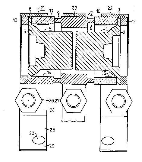
6 Essentially, the overvoltage charge eliminator shown in Figure
l consists of the two cylindrical end electrodes 1 and 4, the
middle electrode 7 that is arranged concentrically to them,
and the two hollow cylindrical ceramic bodies 10 and 11. The
end electrodes 1 and 4 are of copper, are essentially
ll cylindrical, and have a foot section 2 or 5, respectively,
that becomes a ~oldering flange 3 or 6, respectively. The
hollow cylindrical middle electrode 7 is provided on the
insi=de peripheral surface at both ends with a radial step 8
and with a similar radial step 9 on the outer peripheral
16 surface. The middle electrode 7 and the insulating body 10
and 11 are soldered to each other at the ends. In the same
way, the insulating bodies 10 and 11 are soldered at the end
faces to the foot sections 2 and 5 of the end electrodes 1 and
4. Contact rings 12 and 13 that are of a material with
21 special coefficients of thermal expansion are soldered to the
soldering flanges 3 and 6 of the two end electrodes.
The two band-like clamps 21 and 22 are arranged on the
periphery of the end electrodes 1 and 4, and the band~ e
26 clamp 23 is arranged on the periphery of the middle electrode
2t867~7
.
7, in order to feed current to the two electrodes 1 and 4.
The width of the clamp bands 21 and 22 is so selected that the
band lies against both the contract ring 12 or 13,
respectively, and on the flange 3 or 6, respectively, and also
encloses the ceramic insulator 10 or 11 for part of its axial
6 length. This has an effect on the electrical field in the
interior of the charge eliminator that is generated, amongst
other things, by the middle starting strip 14 that is attached
to the inside surface of the ceramic insulators 10 and 11
and/or startlng strip 15 that is bonded alternately to the
ll middle electrode 7 and an end electrode 1 or 4, respectively.
In the present case, the band-like clamps 21 and 22 enclose
the adjacent ceramlc insulators 10 or 11, in each case to 70
per cent of its axial length.
16 Essentially, the band-like clamps 21, 22, and 23 consist of a
tinned copper band that is fixed to the periphery of the
charge eliminator by means of a toggle fastener. The toggle
fastener consists in this instance of a bolt 26 and a nut 27
between which the two ends 24 and 25 of the band are clamped.
21 This means that the band end 25 simultaneously forms a contact
tab 29 that ircorporates a soldering hole 30.
Figure 2 shows how the band clamps 21, 22, and 23 completely
encircle the two end electrodes and the middle electrode
26 around their peripheries.
2~ 86707
Figure 3 shows that an additional section of band 28 is fitted
in the toggle fastener for the band clamp 23 of the middle
electrode; one end of this section 28 of band lies against the
band end 25 of the band clamp of the middle electrode, and it
other end it is shaped as a push-in type contact 31.