Note: Descriptions are shown in the official language in which they were submitted.
21 ~6970
ELECTRONIC DEVICES HAVING REDUCED DESTRUCTION OF
INTE~AL ELE~fENTS UPON MALFUNCT~ON
BACKGROUN~ OF THE INVENTION
The present invention relates generally to electronic devices employing therein
an electronic element with opposite electrodes on its principal planes, and moreparticularly, to electronic modules with an elastic support mechanism for an electronic
element mounted therein having spring contact pieces in contact with respective
electrodes of the electronic element for elastic support of the element as interposed
therebetween.
Conventionally, many electronic devices include positive thermistor devices for
use in current limiter circuitry. Thus, thermistor devices have been widely used in
the manufacture of several types of electric circuitry or modules, including motor
activation controller circuitry for electric refrigerators, electronic demagnetization
circuitry for television receivers, monitor display tube units, and other applications.
One typical configuration of a prior art positive thermistor device is shown in
Figs. 13 and 14, wherein this device is generally designated by the numeral 1. This
conventional positive thermistor device I essentially consists of a casing body or base
3, a positive thermistor element 4 held therein, a pair of first and second terminal
members 5, 6, and a lid or cover 2 attached to the base 3 to close the upper opening
thereof.
As shown, the positive thermistor element 4 exhibits a disk-like shape having
opposite surfaces on which first and second electrodes 7, 8 are disposed respectively.
This positive thermistor element 4 is centrally inserted into the inside space of the
base 3, with the electrodes 7, 8 facing the right and left sides thereof, as shown in
Fig. 14.
The first and second terminal members 5, 6 are assembled within the inside
space of casing base 3 in such a way that these members 5, 6 support both sides of
the opposed elèctrodes 7, 8 of the positive thermistor element 4. Each terminal
member 5, 6 may be an elastic conductive plate of a chosen metallic material. The
2l8697o
first terminal member 5 includes a pair of spring contact pieces 9, 10 having a W-
shaped profile as a whole, and also a hollow tube socket 11 with a longitudinal gap
for receiving therein a known connector pin (not shown) associated therewith to
provide electrical connection therebetween. A wave shaped plate constituting the W-
5 shaped spring contact pieces 9, 10 and the socket 11 may be integrally formed in theterminal member 5 by known welding or caulking techniques. The second terminal
member 6 is similar in structure to the first terminal 5; it has W-shaped spring contact
pieces 12, 13 and connector-pin socket 14.
After assembly within the casing base 3, the spring contact pieces 9, 10 of the
10 first terminal member 5 serve to apply compressive force onto the first electrode 7
due to its inherent elastic nature. Similarly, the spring contact pieces 12, 13 of the
second terminal member 6 apply compressive force to the second electrode 8. Thismay enable the positive thermistor element 4 to be elastically supported or suspended
between the terminal members 5, 6 while the element 4 is interposed between one
pair of spring contact pieces 9, 10 and the other pair of contact pieces 12, 13.Additionally, a mica plate 15 may be disposed around the outer periphery of
the positive thermistor element 4. This mica plate 15 exhibits a circular shape. When
engaged with the outer periphery of thermistor element 4, this plate 15 acts to
facilitate appropriate positioning (hereinafter referred to as "position-determination")
20 of thermistor 4 inside base 3.
After the positive thermistor element 4 and terminal members 5, 6 are
assembled within the casing base 3, the cover 2 is attached thereto so that it closes the
upper opening of the casing body 3. This cover 2 is a rectangular plate member
having at its two corresponding corners two holes 16, 17 to permit insertion of
25 external connector pins into the sockets 11, 14 through these holes respectively.
Another prior known positive thermistor device la is shown in Figs. 16 to 18.
As is readily seen by comparison of the illustration of Fig. 16 to that of Fig. 14, this
prior art device is similar in structure to the previous device; accordingly, like
reference characters are used to designate like parts or components with a redundant
30 explanation thereof being omitted herein.
2l8697o
As can be seen from Fig. 16, the positive thermistor device la is structurally
different from that of Fig. 14 to the extent that a first terminal member Sa has a W-
shaped pair of spring contact pieces 9a, lOa extending vertically, rather than
horizontally as in the previous prior art device l, best shown in Fig. 14, thereby
5 preventing these contact pieces 9a, lOa from directly opposing their associated spring
contact pieces 12, 13 of the other, second terminal member 6. Such vertical facing
relation of spring contact pieces 9a, lOa versus the opposite spring contact pieces 12,
13 may also be seen in Figs. 17 and 18. Figs. 17 and 18 show a plan view and side
view, respectively, of the device shown in Fig. 16.
With the prior art positive thermistor devices l, la, after a long time has
elapsed after installation thereof, the structure of the positive thermistor element 4
may become physically degraded. If this is the case, abnormal heat generation may
take place therein causing sparks to occur during operation, which results in the
positive thermistor element 4 being destroyed due to occurrence of such sparks.
When the thermistor element 4 is destroyed, it breaks into several fragments that can
~isperse within the closed inside space as defined by the casing base 3 and cover 2
attached thereto.
Such a "malfunction mode" phenomenon can lead to a more serious
malfunction mode, which will be discussed in more detail below with reference toFigs l5A and 15B for the positive thermistor device of Figs. 13 and 14, and withreference to Figs. 19 to 21 for the device la shown in Figs. 16 to 18, respectively.
In the positive thermistor device l of Figs. 13 and 14, when sparks occur, the
resulting positive thermistor element 4 experiences occurrence of several cracks 18
therein, as shown in Fig. 15A. Even under such a condition, specific cracked
portions l9, each of which is elastically supported by the opposed spring contact
pieces 9, 10 (or 12, 13) at its opposite sides, continue to stably be held thereat as
shown in Fig. 15B, while the remaining fragments disperse. Accordingly, a power
supply may continuously be fed by way of such residual components 19 of the
thermistor element 4, causing these residual components 19 and their associativespring contact pieces 9, 10, 12, 13 to melt, in turn producing an alloy that exhibits
some conductivity. As a result, an electrical short can be formed between the
- 21 86970
terminal members 5, 6. This adversely serves to accelerate further generation ofabnormal heat. This will possibly torce the device to go into a further malfunction
mode which can, in turn, lead to unwanted softening of the casing base 3.
Furthermore, in the positive thermistor device 1, since the mica plate 15 is
5 arranged therein, certain peripheral portions 20 of the positive thermistor element 4
which are directly in contact with the mica plate 15 tend to also be prevented from
flying away as fragments, in most cases. Such peripheral portions 20 also contribute
to the formation of alloy together with the aforementioned portions 19 being
elastically supported by spring contact pieces 9, 10, 12, 13, with the result of10 increasing the amount of materials for producing the alloy. This may exacerbate the
malfunction of the device, which may cause the softening of base 3 to become more
senous.
On the other hand, in the positive thermistor device la shown in- Figs. 16 to
18, the positive thermistor element 4 experiences occurrence of cracks 21 due to15 generation of sparks, as shown in Fig. 20A. In this case, the therlllistor element 4 is
broken into several fragments that tend to disperse. At this time, since the spring
contact pieces 9a, 10a and their opposed contact pieces 12, 13 are not identical to
each other in a spring-force application direction, any dispersed fragments will be
positionally offset from their original positions. However, since the distance 22
20 between a respective one of the spring contact pieces 9a, 10a and a corresponding one
of opposed spring contact pieces 12, 13 associated therewith is designed so that the
distance is less than the thickness 23 of the positive thermistor element 4 in a free
state where the element 4 is removed as shown in Fig. 19, one part 24 thereof will
possibly be held at its original position as a result of the fact that it happens to be
25 gripped or hung between the spring contact piece 9a and/or 10a on one hand and
elements 12 and/or 13 on the other hand, as shown in Figs. 20A and 20B. If this is
the case, application of a power supply may continue via such a hung portion 24
causing, in a similar way as in the previous device 1, this portion 24 and any one of
contact pieces 9a, 10a, 12, 13 to melt, in turn producing an alloy, whereby the
30 terminal members 5a, 6 are electrically shorted therebetween so that abnormal heat
generation is accelerated. This, in turn, may lead to a further serious malfunction
2 1 86970
mode where the casing base 3 is softened undesirably. Regarding the presence of the
mica plate 15, the previous discussions may also be true for this device la. Namely,
in the positive thermistor device la, since the mica plate lS is arranged therein,
certain peripheral portions 25 of the positive thermistor element 4 which are directly
in contact with the mica plate 15 are prevented from flying away as fragments in most
cases, as shown in Fig. 20B, in a similar manner as in the above positive thermistor
device 1. Such peripheral portions 25 also give rise to generation of an alloy, which
adds to the amount of material for producing the alloy. This may serve to worsen the
malfunction mode of the device, causing a softening of base 3 to become more
serious.
The aforesaid problems will not exclusively arise with positive thermistor
devices, and will possibly take place in other types of electronic components ordevices, insofar as these other types of components employ therein an electronicelement that is electrically fed and elastically supported by using similar contact
lS members associated therewith, which element is susceptible to degradation and
eventual destruction due to long use.
It is therefore an object of the present invention to provide a new and
improved electronic device capable of avoiding the problems encountered with theprior art.
It is another object of the invention to provide an improved electronic module
capable of attaining high reliability in operation even when destruction takes place at
an electronic element packed therein.
It is a further object of the invention to provide an improved electronic modulecapable of assuring higher operational reliability upon occurrence of destruction of its
internal electronic element packed therein by providing enhanced isolation amongfragments even after physical destruction of the element.
To attain the foregoing objects, the present invention provides an electronic
device which includes an electronic element having first and second opposed
electrodes, and a support structure for elastically supporting the electronic element,
2186970
wherein the support structure specifically includes first and second contact sections in
contact with the first electrode at difterent positions thereon, and third and fourth
contact sections in contact with the second electrode at different positions thereon.
The first and fourth contact sections are located closer to the outer peripheral portions
5 of the first and second electrodes than the third and second contact sections, whereas
the first and fourth contact sections are electrically connected with the first and second
electrodes respectively to provide a conductive path for application of power supply to
the electronic element. The second and third contact sections are electrically isolated
from the first and second electrodes.
In accordance with the principles of the invention, several different
ernbodiments are described herein.
In accordance with one aspect of the invention, the support structure includes afirst conductive terminal member having first and second spring contac~ pieces for
elastically applying compressive force to the first electrode, a second conductive
15 terminal member having third and fourth spring contact pieces for elastically applying
compressive force to the second electrode, a first insulative member interposed
between the second spring contact piece and the first electrode, and a second
insulative member interposed between the third spring contact piece and the second
electrode, wherein the first spring contact piece, the first insulative member, the
20 second insulative member and the fourth spring contact piece correspond to the first to
fourth contact sections respectively.
In accordance with another aspect of the invention, the support structure
incl~ldes a first conductive terminal member having a first spring contact piece for
elastically applying compressive force to the first electrode, a first insulative member
25 in contact with the first electrode, a second insulative member in contact with the
second electrode, and a second conductive terminal member having a second springcontact piece for elastically applying compressive force toward the second electrode,
wherein the first spring contact piece, first insulative member, second insulative
member and second spring contact piece may correspond to the first to fourth contact
30 sections respectively.
21 86970
The electronic device may further include a casing structure for holding thereinthe electronic element and the first and second terminal members, wherein the first
and second insulative members are associated with the casing.
With such an arrangement, when the electronic element is accidentally
S destroyed due to degradation through long use, respective residual fragments that are
elastically supported by both the first and fourth contact sections and by the second
and third sections are acted upon by these contact sections so that such portions may
be forced in the condition where the principal plane of the electronic element is
deviated in position. Furthermore, these residual portions remain interposed either
10 between the first contact section being rendered electrically conductive and the third
contact section rendered insulative, or between the fourth contact section rendered
electrically conductive and the second contact section rendered insulative. Thiseliminates any current flow therethrough, enabling the resulting circuitry to be forced
into the open state.
In accordance with yet another aspect of the invention, an electronic module
includes an electronic element having first and second principal planes opposed along
a thickness dimension thereof, and first and second electrodes formed on the first and
second principal planes respectively, a pair of a first conductive spring contact piece
and a first insulative position-alignment projection in contact with the first principal
20 plane at different positions thereon, and a pair of a second conductive spring contact
piece and a second insulative position-alignment projection in contact with the second
principal plane at different positions thereon. The first and second spring contact
pieces are elastically in contact with the first and second electrodes respectively, while
providing an electrical conductive state therebetween. The first spring contact piece is
25 located closer to the outer periphery of the electronic element than the second
position-alignment projection, while causing the first spring contact piece to oppose
the second position alignment projection, with the electronic element being interposed
therebetween. The second spring contact piece is located closer to the outer periphery
of the electronic element than the first position-alignment projection, while causing the
30 second spring contact piece to oppose the first position alignment projection, with the
electronic element being interposed therebetween.
2 1 86970
In the above structure, a significant exemplary feature of the invention is thateach of the first and second spring contact pieces defines a spring force having a
direction generally directed outward relative to a direction which is perpendicular to
the principal planes (which is henceforth referred to as the "direction of thickness of
5 the electronic element"). In other words, the structure of the electrical device forces
fragments outward toward the peripheral portions of the electronic element.
Another significant feature of the invention is that each of the first and second
position-aligmnent projections has a tip end being partly cut away at its outer side
facing the outer periphery of the electronic element.
It should be noted that any number of the above features may also be
structurally combined together.
Preferably, the electronic module embodying the invention may further include
a housing or casing for holding therein the electronic element and the first and second
spring contact pieces, while the first and second position-alignment projections are
associated with this casing.
Additionally, the principles of the invention may advantageously be applied to
the manufact-lre of electronic devices or modules employing therein a positive
thermistor element as an internal electronic element, the modules being also known as
positive thermistor devices.
A significant advantage of the invention is that even when the electronic
element inside the device is accidentally cracked to induce physical destruction during
operation, any continuous flow of abnormal current therein can be successfully
suppressed or eliminated by forcing the destroyed electronic element tO be in the open
state immediately after such an accident, thereby ensuring that maxilnized safety is
guaranteed.
More specifically, the electronic device includes an elastic support mechanism
for elastically supporting or suspending the internal electronic element inside the
device, which mechanism includes a plurality of pairs of spring contact pieces and
position-determination projections. While all of these pieces and projections cause the
element to be interposed between each contact and its corresponding projection on the
opposite side of the element, only spring contact pieces contribute to formation of an
21 86970
electrically conductive path for power supply of the element, whereas the projections
are merely mechanically in contact with the element for position-determination
thereof. In other words, looking at each pair of contact piece and projection on the
opposite sides of the element tor support thereof, only one of them is electrically
S coupled to the element while the other remains insulated from it. Accordingly, when
the element is cracked and destroyed into fragments due to the degradation of its
material, even if some of the fragments attempt to remain at their original positions
due to application of elastic or compressive forces from a corresponding contactpiece-projection pair, a conductive path will no longer be defined for each residual
tragment because ot the fact that one of its associated support members (namely, the
projection) must be an electrical insulator, which acts to interrupt or cut off any
possible contimlolls flow of current through the fragment(s). This can ensure that the
electronic element being presently destroyed is in the open state with respect to any
one of such residual fragments, if any. Therefore, it is possible to reliably eliminate
unwanted transition of the element into more dangerous malfunction states otherwise
occurring in such a way that residual fragments and spring contact pieces adversely
cooperate to induce undesired alloying phenomenon, creating electrical short-circuiting
that accelerates further generation of abnormal heat in the element destroyed.
Another significant advantage of the invention is that safety can be much
enhanced upon occurrence of destruction of the element due to the fact that the elastic
support mechanism is specifically arranged so as to force adjacent ones of residual
fragments to become spaced apart from each other, thereby minimizing the possibility
of shorting between the elements. This can advantageously serve to prevent current
flowing between adjacent ones of fragments inside the casing structure.
A filrther advantage of the invention is that the aforesaid sat-ety enhancement
features also serve to allow the casing structure to be constituted from resin material,
thus reducing cost and structural complexity, while eliminating softening thereof
otherwise arising upon receipt of abnormal heat due to continuous flow of abnormal
current after destruction of the element. The advantages may typically become more
significant when the invention is applied to positive thermistor devices.
21 86970
These and other objects, features and advantages of the invention will be
apparent from the following more particular description of preferred embodiments as
illustrated in the several figures of the drawings.
Fig. I is a front view of a positive thermistor device in accordance with one
embodiment of the invention.
Fig. 2 is a plan view of the positive thermistor device shown in Fig. 1.
Fig. 3 is a bottom view of the positive thermistor device of Fig. 1.
Fig. 4 is a left side view of the positive thermistor device of Fig. 1.
Fig. 5 is a perspective view of the positive thermistor device showing a casing
cover as separated from the remaining parts thereof to visually reveal the inside
structllre of the device.
Fig. 6 illllstrates in an exploded manner several parts assembled in the positive
lS thermistor device of Fig. 1.
Fig. 7 is a plan view of the positive thermistor device showing its main parts
inside the thermistor device of Fig. 1.
Fig. 8A and 8B show plan views at major steps of a process where the positive
therlllistor device of Fig. 7 experiences occurrellce of cracks which reslllt in20 destruction.
Fig. 9 is a front view of the positive thermistor device of Fig. 1 showing its
main parts as arranged inside the device.
Fig. 10 is a diagrammatical representation for explanation of the relation
between the positive thermistor device of Fig. 9 and its associated position-alignment
25 projections.
Fig. I l is a diagrammatical representation for explanation of a planar
positional relation of the positive thermistor versus position-alignment projections
shown in Fig. 9.
Fig. 12 is a side view of the embodiment for explanation of the contact state of30 the positive thermistor with the position-alignment projections of Fig. 9.
21 86970
Fig. 13 is a plan view of one prior art positive thermistor device, with a coverthereof being removed for purposes of illustration.
Fig. 14 is a perspective view of the prior art device of Fig. 13, wherein parts
or components thereof are illustrated in an exploded manner.
Figs. 15A and lSB show front views of the prior art device of Fig. 13 at
major steps of a process where the prior art device experiences occurrence of cracks
which result in destmction.
Fig. 16 illustrates an exploded perspective view of another prior art positive
thermistor device.
Fig. 17 is a plan view of the major part of the prior art device shown in Fig.
16 for explanation of the positional relation of a positive thermistor element and its
associated spring contact pieces.
Fig. 18 is a side view of the major part of the prior art device shown in Fig.
16 for explanation of the positional relation of a positive thermistor element and its
associated spring contact pieces looking at the device from the electrode formation
side of the positive thermistor element.
Fig. 19 is a plan view of the major part of the prior art device of Fig. 16 for
explanation of the dimensions and positioning of the spring contact pieces, with the
thermistor element removed.
Figs. 20A and 20B show front views of the positive thermistor element in the
prior art device shown in Fig. 16 at major steps of a process in which this element
experiences occurrence of cracks which result in destruction.
Fig. 21 shows a destruction state of the prior art positive thermistor element
having cracks as shown in Fig. 20A, when looking at the device from the right side of
the structure of Fig. 20B.
Fig. 22 is a plan view of an electronic module in accordance with another
preferred embodiment of the invention, with a cover thereof being removed for
purposes of illustration only.
Fig. 23 is an exploded perspective view of the electronic device shown in Fig.
22.
21 86970
Fig. 2~ is a plan view of a positive thermistor element provided in the
electronic module of Fig. 22 for visual indication of cracks due to occurrence of
sparks therein.
Fig. 25 is a plan view of the positive thermistor element thus destructed when
5 cracks occurred.
Fig. 26 is a plan view of an electronic module in accordance with still another
embodiment of the invention, with its cover being removed for purposes of illustration
only .
Fig. 27 is an exploded perspective view of the electronic Module shown in Fig.
10 26.
A positive thermistor device in accordance with one embodiment of the present
invention is generally designated by the nllllleral 31 as shown in Figs. 1 through 12.
Referring to Fig. 1, the positive thermistor device 31 has a casing structure 32consisting of a base 33 and a lid or cover member ~4. The thermistor device 31
includes a positive thermistor element 35 as held therein, and a pair of terminal
members 36, 37, one of which is shown in Fig. 1, and both of which are visible in
Fig. 3, for example. A perspective view of the resulting assembly is best illustrated
in Fig. 5.
The casing base 33 and its cover 34 are made of a chosen heat-resistant
incombustible material that offers incombustibility equivalent to the level "94V-O" of
the UL standards, such as phenol, polyphenylenesulfite, polybutylene terephthalate, or
the like. The base 33 is structured to have a projection on the bottom thereof
25 enabling the positive thermistor element 35 to be stably held therein. As will be
discussed in detail below, the base 33 and cover 34 may be provided with severalconfigurations for enabling precise position-determination or aligmnent of the positive
thermistor element 35 and terminal members 36, 37 once assembled thereto.
The positive thermistor element 35 may be made of a chosen ceramic-like
30 semiconductor material with Curie temperature of approximately 130~C, which is
formed into a coin- or disk-like shape. This disk-like positive thermistor element 35
2~ 86970
has first and second principal planes on the opposite sides thereof, on which two, first
and second electrodes 38, 39, are formed respectively. These electrodes 38, 39 may
be a lamination of an underlying nickel (Ni) layer and an overlying silver (Ag) layer.
Preferably, the underlying layer is exposed at the periphery of the overlying layer for
5 elimination of unwanted migration of Ag material. Note that the positive thermistor
disk 35 may alternatively be formed into another shape, including rectangular plate,
bead, or rod. The two-terminal positive thermistor disk 35 is vertically inserted
centrally into the inside space of the base 33 with its electrodes 38, 39 laterally facing
each other.
As shown in Fig. 5, the first and second terminal members 36, 37 are also
pacl;ed into the base 33 in such a manner that the positive themlistor disk 35 is
interposed therebetween. These terminals 36, 37 are made of a chosen metallic
material with excellent conductivity.
More specifically, as better seen from an exploded perspective view depicted
in Fig. 6, the first terminal member 36 has a spring contact piece 40 made of a thin
tolded metal plate, and a conductive side-slit hollow tube socket 41 that receives a
known external connector pin (not shown) to provide electrical interconnection
therebetween. The first terminal 36 also has a downward extending fastener edge 42
tor rigid insertion into a corresponding receptacle of the base 33. In the embodiment
20 shown in Figs. I to 12, thin metal plates for the spring contact piece 40 and pin
socket 41 are separately prepared and later assembled together by known welding or
caulking techniques into an integral terminal component. The metal plate for spring
contact piece 40 may be a copper-titanium (Cu-Ti) base plate with a Ni overcoat as
formed by metal plating techniques. The metal plate of socket 41 may be a Cu-Ni
25 plate.
As best shown in Fig. 6, the second terminal member 37 is constituted from
an H-shaped plate structure that consists of a spring contact piece 43, a pair of
connector-pin sockets 44 at the top portions of the "poles" of the H-shape, 45 and a
pair of downward extending fastener edges 46, 47 at the bottoms of such poles of the
30 H-shape. This H-shaped two-pin terminal 37 is similar to the first terminal 36 in
material and in manufacture.
2 1 86970
Once assembled, the first terminal me~ber 36 (for purposes of convenience,
this one-pin terminal 36 will be referred to as the "I-shaped" terminal hereinafter due
to the fact that it has only one upward ext~nding pole as a whole, to tacilitatedistinguishing over the two-pin terminal 37 is position-determined by a wall 48 inside \/
the base 33 as shown in Fig. 6, causing its fastener edge 42 to vertically project out
of the outer surface of base 33, as can be seen from the illustration of Fig. 5, for
electrical connection with any external circuitry operatively associated therewith. To
permit insertion of an external connector pin (not shown) into the socket 41 of the I-
shaped termil1al 36, the casing cover 34 has a corresponding hole or opening 49
therein.
Likewise, the assembled H-shaped terminal 37 is position-determined by
another wall 50 inside the base 33, while allowing its fastener edges 46, 47 to
externally project downward from the base 33, as shown in Fig. 5, for providing
electrical connection with external circuitry. The cover 34 has therein a hole or
lS opening 51 also, for permitting an associative contact pin to exten1ally penetrate
therethrougl1 to mate with a selected one of the sockets 44, 45. Note here that the
cover 34 has no opening for the remaining nonselected socket (here, socket 45) simply
because it remains unused in the illustrative embodiment. In this respect, this socket
45 may be removed as necessary.
Preterably, the holes 49, Sl are minimized in diameter while allowing external
connector pins used to pass through the holes. This may provide-an enhanced sealed
environment inside the casing 32, thereby enabling the positive thermistor device 31
to offer improved resistance against the atmosphere.
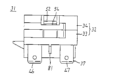
To also enhance the sealed environment inside the casing 32, the base 33 and
cover 34 are tightly coupled together. To do this, the base 33 has two hooks 52,whereas the cover 34 has corresponding recesses 54 rigidly engageable with hooks 52.
With these members, base 33 and cover 34 may be readily engaged and combined
with each other in a snap-like fashion to provide an integral air-tight casing structure.
Furthern1ore, the base 33 has a rib 55 along its opening peripheral edge, while the
cover 34 has a corresponding recess (not shown) for receiving the rib 55 on the
opening peripheral edge thereof.
2~ 86970
The position-alignment scheme as employed t'or the positive thermistor disk 35
inside the casin~ 32 is as follows.
See Fig. 7, which depicts a plan view of the positive thermistor device 31 afterassembly, with several parts or components being removed to reveal the internal
5 structure thereof for pllrposes of illllstration only. The casing base 33 is a walled
enclosure having position determination projections 56, 57 standing upright from the
bottom of the walled enclosure. These projections cooperate with the spring contact
pieces 40, 43 to force the positive thermistor disk 35 to be elastically supported or
suspended by the projections and contact pieces and also interposed therebetween,
10 thus providing precise position aligmnent for attaining a substantially "floating"
suspension of the thermi.stor disk 35 inside the casing 32 as separated from the inner
walls thereof. In the illllstrative elnbodirnent, the casing 32 is designed as shown in
Fig. 4 so that the floating thermistor disk 35 measllres I millimeter (mm) or more in
the distance 76 between it and the inner wall of casing 32, as indicated llsing a broken
15 line in Fig. 4.
More specifically, as best illustrated in Fig. 7, a first pair of the spring contact
piece 40 and one position-alignment projection 56 are arranged to come in contact
with one principal plane of the positive thermistor disk 35, whereas a second pair of
opposed spring contact piece 43 and position-alignment projection 57 are in contact
20 with the opposite principal plane of disk 35, thereby elastically supporting disk 35 as
interposed therebetween inside casing 32. Notably, the first spring contact piece 40
and the second spring contact piece 43 are specifically disposed so that they
diagonally oppose each other, while the first position-alignment projection 56 and
second position-alignment projection 57 cross-diagonally oppose each other, as can be
25 seen from the illustration of Fig. 7. [n other words, a line connecting the opposed
spring contact pieces 40, 43 together crosses a line connecting projections 56, 57, to
horizontally define an X-shaped line combination.
In this situation, the spring contact pieces 40, 43 are elastically in contact with
the opposite electrodes 38, 39 of thermistor disk 35 to provide electrical connection
30 therebetween. The position-alignment projections 56, 57, which are formed integrally
2 1 86970
16
with base 3~ are electrically insulative, so that these constitute insulative contacts with
disk electrodes 38, 39.
It is also important that while the first spring contact piece 40 opposes the
second position-alignlnent projection 57 with the thennistor disk 35 being interposed
therebetween, contact 40 is at an outer position closer to the periphery of disk 35 than
its corresponding projection 57. The same applies with respect to the other
combination of the second spring contact piece 43 and the first position-alignment
projection 56. Contact piece 43 is at a position closer to the opposite periphery of
disk 35 than projection 56 as shown in Fig. 7. With this "outer offset positioning"
feature of spring contacts 40, 43, the resulting application of spring force to disk 35
directs outward relative to the direction of thickness of disk 35, as designated by
arrows 58 in Fig. 7.
It is a further important exemplary feature of this embodiment that the first and
second position-alignlllent projections 56, 57 have slanted cut-away portions 60, 61 at
their tip ends. ~lore specifically, the sides of the projections 56, 57 closest to the
peripheral portions of the disk 35 are slanted. These cut-away portions 60, 61 may
advantageously serve to increase or maximize efficiency and/or workability of the
spring force as applied from respective contact pieces 40, 43 toward the radially
opposed peripheral edges of disk 35 along the outward directions as indicated byarrows 58 in Fig. 7.
After long use of the positive thermistor device 31, it may happen that its
internal thermistor disk 35 experiences occurrence of cracks due to material fatigue
thereof. In the worst case, the disk 35 can be destroyed physically. Even if this is
the case, the spring contact pieces 40, 43 and the position-aligmnent projections 56,
57 for elastic support of the disk 35 may advantageously serve to suppress or
eliminate occurrence of any continuous flow of abnormal current therein due to the
presence of a short-circuit, resulting from electrical shorting of residual fragments
after destmction. The operation of the contact pieces 40, 43 and the projections 56,
57 is as follows.
See Fig. 8A, which diagramlllatically illustrates one exemplary occasion where
cracks 62 take place in the positive thermistor disk 35 along the thickness thereof due
- 21 86970
to occurrence of sparks therein causing disk 35 to physically break into severalportions or fragments. In this situation, the compressive forces continue to be applied
toward disli 35 from the spring contact pieces 40, ~3. Accordingly, certain fragments
must be present which remain interposed between contact pieces 40, 43 and
projections 56, 57 inside the casing 32. One specific fragment 63 is elasticallysupported by the first spring contact piece 40 and its opposite projection 57, and
another fragment 61 is supported by the second contact 43 and projection 56 as shown
in Fig. 8B. Note here that the remaining fragments of disk 35, including one
~ragrnent 67 indicated by the broken line in Fig. 8B, have brol~en away because of the
fact ~hat no sllch elastic support members secure them reside at their original
posltlons.
Under the condition as demonstrated in Fig. 8B, the spring contact pieces 40,
43 connected with the opposite electrodes 38, 39 of the thermistor disk 35 are
prevented from directly opposing each other via the disk 35, while inhibiting creation
lS of any current flow path that extends from the first spring contact piece 40 through
residual disk tragments 63, 64 to the second spring contact piec~ 13. This can ensure
that any possible current flow or power supply is interrupted or cut off, ensuring that
the internal circuitry ot positive thermistor device 31 is in the open state, that is,
rendered electrically nonconductive.
Hence, a significant exemplary advantage of the positive thermistor device 31
embodying the invention is that, even when power is being supplied to the internal
thermistor disl; 35 after destmction thereof, since the operator cannot be aware of the
interior state of the device 31, it becomes possible to reliably eliminate the transition
of the device 31 into a more dangerous malfunction stage. This stage may otherwise
occur due to the presence of continuous flow of abnormal current that results from the
fact that the residual fragments 63, 64 adversely act to produce an alloy together with
spring contact pieces 40, 43 upon continuous application of power supply to provide
an electrically shorted state, inducing such abnormal heat inside the sealed
environment ot' the positive thermistor device 31.
Anotller significant advantage of the illustrative embodiment is that any
residual fragments 63, 64 between contacts 40, 43 and projections 56, 57 can be
2 1 86970
18
forced to deviate or oft'set in position so that they disperse tar apart from each other
inside the device 31. It has been stated that the direction of action of spring forces
induced by spring contact pieces 40, 43 are specifically arranged to direct outward
relative to the thickness direction of the thermistor disk 35, as demonstrated by use of
arrows 58, 59 in Fig. 8B, whereas projections 56, 57 have specific slanted cut-away
portions 60, 61 at the outer periphery of their tip ends. The combination of such
structllral features serves to force the residllal fragments 63, 64 elastically supported
by contact pieces 40, 43 and projections 56, 57 to disperse far away from each other
as indicated by fat arrows 65, 66 in Fig. 8B.
The foregoing "fragments' outward separative movement" feature may
advantageously act to further enhance the possibility of achievement of an electrical
open state inside the thermistor device 31 after accidental destmction. Specitically,
even when an "intermediate" fragment 67 of Fig. 8B that is free from any elasticsupport remaills between two elastically supported ~ragments 63, 64, these fragments
63, 64 are forced to disperse far away from each other, preventing any possible
electrical contacts from arising between the intermediate fragment 67 and its
neighboring tragments 63, 64, so that an electrical short-circuit will no longer take
place therebetween. Additionally, in most cases, the intermediate fragment 67 will
break away due to the "separative movement" of its neighboring fragments 63, 64.Also, these fragments by themselves tend to break away due to positional deviation
along the arrows 65, 66 inside the thennistor device 31.
The description regarding the device 31 continues with reference to Fig. 9,
which shows a side view of the interior of device 31, with several parts omitted from
the device for purposes of illustration only. As shown, the casing base 33 is provided
with upward extending position-control projections 68, 69 that extend from the bottom
thereof, whereas the cover 34 has similar downward extending position control
projections 70, 71 to oppose base projections 68, 69. These vertical projections 68-71
are provided to ensure that even when the internal thermistor disk 35 happens topositionally deviate due to vibrations in the direction of its principal planes, such
deviation continues to fall within a predefined range. This may suppress or eliminate
occurrence of the shorta~e of current-flow capacity at terminals which will otherwise
-- 2 1 86970
19
occur dlle to positional deviations of spring contact pieces 40, 43 with respect to
terminals 38, 39 of the thermistor device 31.
The positional relation of such projections 68-71 can be better seen from Figs.
10 and 11. Fig. 10 shows another side view of the interior of thermistor device 31
5 with an edge of disk 35 depicted as a front part; Fig. I l depicts a plan view of the
device. As shown in Fig. 10, the disk 35 is secured by upper (cover) and lower
(base) projections 68-71 at the four corner edges thereof. As best shown in Fig. 11,
looking at the device from the upper side, these projections 68-71 are cross-disposed
inside casin~ 31 in such a manner that base projections 68, 69 diagonally oppose each
10 other along one planar diagonal line, while cover projections 70, 71 cross-diagonally
oppose each other along the another diagonal line.
It can be seen from viewing Fig. 10 that the projections 68-71 have slanted
cut-away planes 72-75, respectively, to provide a pin-point contact arrangement for
support of clisk 35 at its four circumferential corner edges.
A signiticant advalltage as derivecl from the position-control projections 68-71is that the thermistor device 31 can be ~reatly improved in satety. More specifically,
the casing 31 may become partly carbonized at positions near the thermistor disk 35
due to occurrellce of sparks as induced by accidental destruction thereof, resulting in a
decrease or degradation in tracking performance, which in turn leads to formation of
an undesirable conductive path that may permit continuous flow of abnormal current.
As an example, position-control projections 68-71 can be carbonized due to sparks
causing a conductive path to be defined therein. If this is the case, the thermistor disk
35 will deviate positionally in the direction of its principal planes. For instance, as
shown in Fig. 12, the disk 35 happens to come in contact with the diagonally opposite
projections 68, 70. Even under this condition, since each of these projections 68, 70
is prevented from extending in a direction in which disk 35 can be short-circuited
along the thickness thereof, no conductive path will take place between the electrodes
38, 39 of disk 35, irrespective of whether projections 68, 70 are actually carbonized
or not. This mav promote enhancement in safety during extended operation of device
31.
21 86970
Tllrnin;, back to Fig. 6, the spring contact pieces 40, 43 are narrowed in widthat most portions as compared with a contact tip portion for electrical contact with the
electrodes 38, 39 of disk 35, as indicated by the n~mlerals 77, 78 with respect to one
contact piece 40 shown. The explanation continues as to one spring contact piece 40,
5 but the same disc~lssion applies to the other piece as well. Such width difference may
shorten (see Fi;,. 9 again) the vertical size 80 of a slit 79 that is defined at a wall 48
(see Fig. 6) in base 33 for penetration of spring contact piece 40 therethrough. This
may advantageously serve to s~lppress generation of air flow between a space forholding therein the sociiet 41 coupled to opening 49 and a space for supporting disk
10 35, thus enhancing the atmospllere-restricting characteristics of the device 31. Yet on
the other hand, it is possible to retain sufficient capacity for current flow at such
contact sections for the reason that a relatively greater width 77 can be maintained for
the exact contact tip end of contact piece 40 with electrode 38.
In this embodilnent, as can be seen frolll Figs. 1, 3 and 4, a rib 81 is arranged
15 on the ollter s~lrtace of the casing base 33 so as to partition the base bottom into two
areas: one tor projection of the fastener edges 42, 46, and the other for projection of
tastener edge 47. This rib 81 acts to lengthen the creepage distance between fastener
edges 42, ~16 and edge 47, thus enhancing the tracking resistant performance andextemal voltage withstanding characteristic therebetween, which may in t~lrn lead to
20 improvemellts in reliability and safety of the thermistor device 31. The presence of
such rib 81 may also be eft'ective to decrease the surface temperature of casing 32 in
the vicinity of tastener edges 42, 46, 47. The rib 81 can further contribute to
suppression of bowing which may occur during molding of casing base 33, thus
improving the accuracy of engagement of the base 33 with the cover 34 so that its
25 resistance to the atmosphere can be improved accordingly.
A positive thermistor device in accordance with another embodiment of the
invention is generally designated by the nulneral 21 in Figs. 22 and 23. This device
21 is generally similar in stmctllre to the thermistor device 31. It includes a casing
base 22, a positive thermistor element 23, terminal members 24, 25, and a cover 26
30 for clos~lre of an upper opening of base 22. In addition to such parts, the device 21
-- 2~86970
has therein electrically insulative square plate members 27, 28 as best shown in Fig.
23.
The base 22 is made of a chosen heat-resistant incombustible material that
oft'ers incombustibility eq~livalent to the level "94V-0" of the UL standards, such as
S phenol, polyphenylenesult'ite, polybutylene terephthalate, or the like. The base 22
may alternatively be made of inorganic resin. The base 22 is structured to have a
projection on part of the bottom thereof allowing the positive thermistor element 23 to
be stably held therein while enabling suitable position-determination of terminals 24,
25 and insulative plates 27, 28 therein.
The therlllistor element 23 is t'ormed into a disk-like shape, with electrodes 29,
30 disposed on the opposite sides thereof. The element 2~ may alternatively be
t'ormed in another shape, s~lch as a rectangular plate. Each electrode 29, 30 may be a
lamination of an underlying Ni layer and an overlying silver Ag layer. 'Preferably,
the ullderlying layer is exposed at the periphery of its overlying layer for elimination
of migration of Ag material. The two-terminal positive thermistor disk 35 is centrally
inserted into the inside of base 22 with its electrodes 29, 30 laterally disposed from
each otller.
One terminal menlber 24 has a pair of spring contact pieces 101, 102 defining
a W-shaped wing, and a socket 107 receiving therein an external connector pin (not
shown) to provide electrical connection therebetween. A plate constituting the spring
contact pieces 101, 102 and a plate fonning socket 107 are combined together by spot
welding techniques. These pieces 101, 102 may be modified into any other shapes as
necessary. Modifying the shape of pieces 101, 102 may also lead to the possibility of
integral formation of pieces 101, 102 and socket 107.
Similarly, the other terminal member 25 has two spring contact pieces 103,
104 and a socket 108. The first and second terminal members 24, 25 are made of achosen metallic material such as stainless steel, copper alloy and the like, thereby
providing the members with appropriate elasticity and electrical conductivity. These
terminals 24, 25 are packed into base 22 while causing thermistor disk 23 to be
~0 elastically disposed between the terminals in the base 22.
2186970
22
As shown in Fi~. 22, the spring contact pieces 101, 102 of the first terminal
21 are positionally shitted from the center toward one side (upward hl the illustration
of Fig. 22) of its corresponding thermistor electrode 29, while causing its elastic or
compressive torce to be applied thereto. The spring contact pieces 103, 104 of the
S second terminal 25 are reversely shitted in position from the center toward the
opposite side (downward in Fig. 22) of its associative electrode 30, while letting its
compressive force act thereonto. This enables thermistor disk 23 to be substantially
in a "floating" condition inside base 22 due to the elastic support applied to both its
sides as attained by cooperation of sequential contact pieces 101, 103, 102, 104.
The rectangular insulative plates 27, 28 are disposed inside the base 22 such
that the first plate 27 is interposed between one piece 102 of the first terminal 24 and
the first electrode 29, ~~hile the other plate 28 is between one piece 103 of the second
terminai 25 and the second electrode 30, as can be readily seen from Fig. 22.
Note that these inslllative plates 27, 28 may be replaced with insulative films
covering selected surt1ce area portions of electrodes 29, 30, whereat corresponding
contact pieces form contacts with the films, or alternatively, replaced by electrically
insulative films or chips made of inorganic or resin material as deposited to partly
cover the outer surface ot pieces 102, 103.
After assembly of thermistor disk 23, terminals 24, 25 and insulative plates
27, 28 into base 22, the cover 26 is attached to close the upper opening of base 22 to
provide a substantially sealed environment therein. For rigid attachment of base 22
and cover 26, an appropriate engagement structure is employed. Cover 26 may be
made of the sa~ne material as base 22. This cover 26 has holes 109, 110 through
which external connector pins (not shown) can pass to be inserted into corresponding
sockets 107, 108.
In the positive thermistor device 21, the terminals 24, 25 and insulative plates27, 28 constitute an elastic support mechanism for thermistor element 23, which
includes supporting contacts tor one thermistor electrode 29 as attained by the spring
contact piece 101 and insulative plate 27, and supporting contacts for the opposite
electrode 30 achieved by insulative plate 28 and spring contact piece 104. Theseelements are specifically disposed at different positions on the opposite electrodes 29,
21 86970
30 in such a manner that insulative plates 27, 28 diagonally oppose each other via the
disk 23 interposed therebetween as shown in Fig. 22, while the first spring contact
pieces 101, 102 and the second spring contact pieces 103, 104 are positionally shifted
toward the opposite side edge portions of disk 23, preventing each piece 101, 102 on
the first electrode 29 from directly opposing a corresponding one of pieces 103, 104
on the second electrode 30 along the thickness of disk 23.
More specifically, the touching position of the spring contact piece 101 on the
first electrode 29, which constitutes a first contact section, is shifted or positionally
offset toward one outer peripheral edge of thermistor disk 23 from the touching
position of its corresponding spring contact piece 103 on the second electrode 30 via
one insulative plate 28 sandwiched therebetween, the piece 103 constituting a third
contact section. Likewise, the touchillg position of the spring contact piece 104 on
second electrode 30, which constitutes a fourth contact section, is shifted to approach
the other outer peripheral edge of clisk 23 from tlle touching position of its
lS correspondhlg spring contact piece 102 on first electrode 30 via the other insulative
plate 27 sandwiched therebetween, the contact piece 102 constituting a second contact
section. This alternate contact-position differentiation schelne provides an
"unsylllmetrical" contact positioning arrangement on the opposite electrodes 29, 30 of
thermistor disk 23.
The spring contact pieces 101, 104 constituting the first and fo~lrth contact
sections are in electrical contact with the opposite thermistor electrodes 29, 30 to
provide a conductive path for power supply to thermistor disk 23. On the other hand,
the insulative plates 27, 28 constituting the second and third contact sections are in
contact (mechanically and electrically insulatively) with electrodes 29, 30, while
permitting no current flow therebetween.
In the positive thermistor device 21, the thermistor disk 23 may be destroyed
due to occ~lrrence of cracks therein as induced by sparks during extended operation.
Even if this is the case, furtller flow of abnormal current can be successfully inhibited
providing enhallced safety, as will be described in detail below.
See Fig. '4, which diagramlllatically represents an exemplary cracked state of
the themlistor disk 23, which leads to physical destruction when disk 23 breaks into
21 86970
several tragments due to cracks 100. ln this example, two fragments remain at their
original positions. One fragment 90 is elastically supported by a pair of springcontact piece 101 and insulative plate 28, and the other fragment 91 is elastically
s~lpported by another pair of spring contact piece 101 and plate 27. The remaining
fragments are dislodged from disk 23. As a result, as shown in Fig. 25, these
residual fragments 90, 91 are acted upon by the contact piece-plate pairs 101, 28 and
104, 27 to deviate the position of the principal planes from each other.
Under this condition, the spring contact pieces 101, 104 in electrical contact
with the electrodes 29, 30 thro~lgh neither of the insulative plates 27, 28, areprevented from directly opposing each other. In addition, these plates 27, 28 provide
electrical insulation to any possible c~lrrent flow paths, one of which paths extends
from spring contact piece 101 thro~lgh resid~lal fragment 90 to opposite contact piece
103, and the other of which paths extends trom contact piece 104 via residual
fragment 91 toward its opposite contact piece 102. Accordingly, the power supplywill be reliably internlpted or cut off with respect to disk 23 immediately after
cracking destruction thereof. Moreover, the residual fragments 90, 91 can no longer
remain in contact with each other d~le to torced positional deviation of the principal
planes, thus rendering the res~lltant internal circuitry electrically nollconductive (in the
open state). This may prevent device 21 from clegracling into any undesirable, more
dangerolls malfunction mode in which the residual fragments 90, 91 of thermistor disk
23 and the temlinals 21, 25 induce alloying phenomena, causing electrical short-circuiting to appear in disk 23, so that generation of abnormal heat further continues
even after destruction thereof.
A positive thermistor device in accordance with a further embodiment of the
invention is shown in Figs. 26 and 27, wherein the device is generally designated by
numeral 21a. This device 21a is similar to that shown in Figs. 22-23 with the
exception that (1) the opposite terminal melllbers 24, 25 are replaced with elements
24a, 25a of dift-erent stmcture, (2) the insulative plates 27, 28 of Figs. 22-23 are
removed, and (3) the casing base 22 is replaced by a base 22a having insulative mold
sections 270, 280 tor attaining ins~llative support of thermistor disk 23 similar to that
provided by plates 27, '8.
- 2 1 86970
I\~Iore specifically, as shown in Fig. 27, the first terminal member 21a has a
single spring contact piece 105, while the second terminal 25a also has a sin~le spring
contact piece 106. These pieces 105, 106 are specifically disposed inside base 22a so
that they diagonally oppose each other via disk 23, as best shown in Fig. 26. The
insulative mold sections 270, 280 of base 22a are formed to define round
protuberances at their tip ends respectively and are disposed to cross-diagonally
oppose each other as shown in Fig. 26 with respect to pieces 105, 106 as shown.
These melllbers 105, 106, 270, 280 may constitute elastic support means for allowing
clisk 23 to be held between one pair of piece 105 and mold protuberance 270 and the
other pair ot piece 106 and protuberance 280. The mold protuberances 270, 280 may
be formed integrally with base 22a, or alternatively be made of separate parts being
attached or fixed to base 22a. It can be readily seen from viewing Fig. 26 that the
spring contact piece 106, protuberances 270, 280 and contact piece 105 are alternately
located on the opposite surtaces of disk ~3.
With such an arrangelnent, similar functions and advantages to those
previously identitied may be achieved, as will be describecl in detail below.
In the positive therlllistor device 21a, the elastic support mechanislll for
elastically supporting thermistor elemellt 23 is constit~lted from termillal members 24a,
25a and base 22a having round insulative protuberances 270, 280. This support
mechanislll includes four, first to fourth contact sections for the first and second
thermistor electrodes 29, 30, which sections are the spring contact piece 105,
protuberances 270, 280 and contact piece 106, wherein contact piece 105 and
protuberance 270 are on electrode 29, whereas contact piece 106 and prot~lberance
280 are on electrode 30. These support elements 105, 106, 270, 280 are located at
different positions on the opposite electrodes 29, 30 in such a manner that any one of
these elements is prevented from directly facing a corresponding one of the other
elements. That is, the touclling point of contact piece 105 on the first electrode 29 is
positionally oftset toward one peripheral edge of disk 23 from that of protuberance
280 on the second electrode 30, as can be seen from Fig. 26, whereas the touching
point of contact piece 106 on the second electrode 30 is positionally offset toward the
-- 21 86970
26
other, radially opposed peripheral ed,,e ot disk 23 from that of protuberance 270 on
the first electrode 29, as shown.
The spring contact pieces 105, 106 constituting the first and fourth contact
sections are electrically in contact with the t~irst and second electrodes 29, 30
S respectively, providhlg a condllctive path tor the power supply to disk 23. On the
other hand, the first and second protllberances 270, 280 constituting the second and
third contact sections are insulatively in contact with electrodes 29, 30.
In the positive therlllistor device 2 la, when the thermistor element 23 is
accidentally cracked due to occurrence of sparks, certain fragments which are directly
supported by one pair ot spring contact piece 105 and insulative protuberance 280 and
also by the other pair ot contact piece 106 and protuberance 270, may remain at their
original positions due to application of compressive forces from the support pairs,
while the remaining fraglnents fall away. Such residual fragments (these may
correspond to tragments 90, 91 of Fig. 24) are given actuating torces causing their
prhlcipal plalles to deviate hl position with respect to each other in a similar manner
to that shown hl Fig. 25.
In the foregoing situation, the sprhlg contact pieces 105, 106 making electricalcontacts with thermistor electrodes 29, 30 are prevented from directly opposing or
tacing each other via the tllerlllistor clisk 23 being interposed therebetweem The
contact piece 105 merely opposes ins~llative protuberance 280, whereas contact 107
opposes protuberance 270. This causes any power supply to be interrupted, rendering
the resulting circuitry nonconductive. It is thus possible, as in the previous
embodiment device 21. to successfully eliminate electrical shorting conditions
immediately after occurrence of abnormality during operation, enabling device 21a to
be protected against a transition to a more dangerous malfunction mode due to further
continuation ot tlow ot abnormal current therein, even after destmction of thermistor
disk 23 inside the casing structure of the thermistor device 21a.
While the inven~ion has been particularly shown and described with reference
to preterred embodiments thereof, it will be understood by those skilled in the art that
various changes in torm and details may be made without departing from the spirit
and scope ot the invention, as defmed by the clahlls which follow.
1 86970
For example, while the positive thermistor device 31 shown in Figs. 1-12
includes the casing 32, this casing may be excluded if an alternative structure is
employed therefor which can support the spring contact pieces 40, 43 and position-
alignment projections 56, 57 while allowing the thermistor disk 35 to be elastically
S supported and interposed therebetween. The same applies with respect to the
embodilllent devices 21, 21a shown in Figs. 22-27.
Also, the "fragment outward separative movement" feature of the invention
does not always consist of both (I) the "spring force outwArd application"
arrangement of pieces 10, 43 as denoted by the arrows 58, 59 of Fig. 8B and (2) the
10 "fragmellts' outer movement acceleration" arrangement of the projections 56, 57 as
attained by formation of the cut-away portions 60, 61 at tip ends thereof. When
appropriate, either one of these arrangements may be employed as needed.
In addition, the principles of the invention are not restricted to the illustrated
therlllistor device 31 including thermistor disk 35. The principles extend to any type
lS of electronic device where it is desirable to prevent a short circuit upon the
occurrence of a malfllnction.