Note: Descriptions are shown in the official language in which they were submitted.
21~~1101
SAFETY CIRCUIT
This invention relates to a safety circuit with an
actuating device for electrical appliances, whereby the
actuation device is capable of being operated by means of
two key buttons or switch stacks. Many different areas of
application are to be understood by the term electrical
appliances, that is, the invention may be applied to all
electrical safety devices with two separate electrical
key buttons or switch stacks used for guard circuits,
such as those used with light grids or guard doors, for
example to mechanical plant, emergency monitoring, limit
switch monitoring, floor mats, light curtains and the
like. Presses, stamping machines, milling machines,
lathes or winding devices may be quoted as examples of
mechanical plant.
In the practice and from the state of the technology,
several designs of safety circuits are known of the type
described above and in fact used in combination with
electrical appliances or machines, where, in the switched
on state, dangerous conditions exist for operating
personnel, in particular dangerous machine motion. A two
handed actuation is used to switch to the dangerous
condition which should guarantee that both hands of the
operator are occupied and every possibility is ruled out
far intervening with either hand in the space where the
danger is being brought about. At the same time, it
should guarantee that the operator or his/her legs are in
a place where there is no danger to the operator during
the dangerous motion. In connection with this one strives
with known safety circuits to ensure that any
21 x.71 ~1
2
manipulation is ruled out by the two handed actuation.
Furthermore one strives to ensure that the safety circuit
works perfectly, so that only then is through switching
at the consumer terminals i.e. switching to the dangerous
operating condition, possible and that on the other hand
if any fault arises within the circuit, through switching
is certain to be prevented. The electrical safety
circuits known until now either do not fulfil all the
safety criteria or they are structured in a complicated
way and are expensive to build so that they require very
high expenditure and a safety risk is apparent in the
complexity of the construction.
The invention is based on the task of creating a
safety circuit with general application and which is
simply and clearly structured therefore signifying low
expense but which however meets all the safety criteria
including the prevention of any kind of manipulation.
To resolve this problem, a safety circuit with the
characteristics of Claim 1 has been proposed.
Therefore the safety circuit essentially comprises
two subassemblies, namely a driver stage and an astable
circuit or multivibr_at:or, with the properties given in
Claim 1.
In an advantageous embodiment of the invention, a
capacitor is provided, which is so dimensioned that, in a
position of equilibrium, it stores the energy that is
required to provide the astable circuit or multivibrator
with a voltage within the maximum 500 ms actuation time
of the two key buttons..
In this connection, it is advantageous that with the
actuation of the two key buttons within an actuation time
of 500 ms, the driver stage is supplied with voltage V+
and V- via the make contacts of the key buttons and the
~~~~1~1
3
relays are activated. In the circuit, the capacitor is
integrated into the astable circuit or multivibrator.
Preferably, the astable circuit or multivibrator
generates square ware signals with an edge steepness of
up to 10 ~s, preferab7.y smaller than 1 ~~s, whereby there
is a pulse duty factor Tin to To"t of 50 o to 50% .
According to a further characteristic of the
invention, a first diode is provided between the first
key button and the driver stage and a second diode is
provided between the second key button (S2) and the
driver stage whereby the diodes block the flow of current
to the driver stage when the key buttons are inoperative.
Furthermore, in an advantageous extension of the
safety circuit according to the invention, it is provided
that the square wave signals from the astable circuit or
multivibrator trigger the driver stage in such a way that
the square wave signals are alternately high and low, so
that either the first or the second relay is energised.
According to a further characteristic of the
invention, it is provided that the astable circuit or
multivibrator are supplied with power via the relay make
contacts if the relays are activated.
Finally with the safety circuit according to the
invention, it is provided that the two complementary
square wave signals persist over similar lengths of time
and are inverse to one another.
A preferred design form of the safety circuit
according to the invention is shown in the drawing, the
structure and function of which is described below.
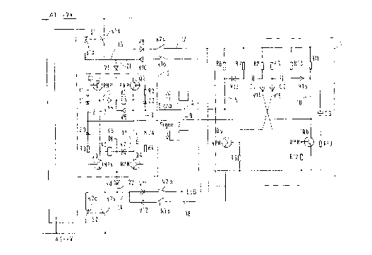
The safety circuits shown in the drawing essentially
comprises a driver stage 2 shown in the rectangle marked
in the dot and dash pattern and an astable circuit or
multivibrator 1 which is similarly enclosed in a
2187iQ1
4
rectangle of dot and dash lines on the drawing and is
connected to the driver stage 2 as will be explained in
detail below.
The driver stage 2 is operated in combination with
two key buttons S1 and S2 of an actuation device, for
example with two handed actuation, not shown in detail.
The two key buttons S1 and S2 are to be operated as
simultaneously as possible, at least within the short
actuation time further commented on in more detail below.
The electrical voltage V+ or V- is supplied to the driver
stage 2 via key buttons S1 and S2. The driver stage 2 has
two PNP transistors Q1 and Q2 and two NPN transistors Q3
and Q4. The bases of the PNP transistor Q2 and the NPN
transistor Q4 are connected to one another by line 3, in
which two resistances R2 and R4 and two Zener diodes Z2
and Z4 are connected in series. Furthermore, between the
Zener diodes Z2 and Z4, which are connected series aiding
and in their conducting direction from resistance R4 to
resistance R2, a line 4 is connected, which connects the
driver stage 2 with the astable circuit or multivibrator
1 and which transmits Signal 1 which will be further
explained in detail below whereby line 4 is connected in
the multivibrator to a line 5, which connects resistance
R6 with the collector of transistor Q5.
Furthermore, the collector of PNP transistor Q2 is
connected to the collector of NPN transistor Q4 via a
line 6. The emitter of NPN transistor Q4 is, on the other
hand, connected to t:he emitter of NPN transistor Q3,
whose collector is connected to the collector of PNP
transistor Q1 by a line 7. The emitter of PNP transistor
Q1 is furthermore ~~onnected to the emitter of PNP
transistor Q2. The PNP transistor Q1 and NPN transistor
Q3 are in addition connected via a line 8 which is
2.1 x.71 ~1
connected to the bases of the previously mentioned
transistors Q1 and Q3. Two resistances are connected into
line 8 between which Zener diodes Z1 and Z3 are
connected. Between Zener diodes Z1 and Z3, line 9 is
5 connected which connects line 8 in the driver stage 2
with a line l0 in the astable circuit or multivibrator 1,
whereby line 10 runs between the resistance R11 and the
collector of NPN transistor Q6. Signal 2 which will be
explained below is transmitted via line 9.
Two relay-diode combinations are connected between
lines 6 and '7, whereby a diode V4 and a relay K1 are
connected in a line 17., whereby the conducting direction
of these diodes runs from the collector of PNP transistor
Q1 towards the collector of NPN transistor Q4. A recovery
diode V5 is connected in parallel with relay K1, whose
conducting direction is opposed to the conducting
direction of diode V4.
The second relay-diode combination comprises a line
12, in which a diode V7 and a relay K2 are connected in
series, whereby the diode V7 is connected on the
collector side of PNP transistor Q2 and the relay K2 is
connected collector side of NPN transistor Q3 and the
conducting direction of diode V7 runs from the collector
of PNP transistor Q2 to the collector of NPN transistor
Q3. Furthermore a recovery diode V6 is connected in
parallel to relay K2 whose conducting direction runs in
opposition to the conducting direction of diode V7.
The key button S1, which in this example is equipped
with collateral contacts, namely a break contact slo and
a make contact sls, i5 connected to the driver stage via
a line 13. In a similar way, key button S2 which is
likewise equipped wir_h collateral contacts, namely a
break contact s2o and a make contact s2s, is connected to
21~7i01
6
the driver stage via a line 14. In lines 13 and 14, which
lead as well to the astable circuit or multivibrator 1,
break contacts alo and k2o are arranged, whereby a diode
V10 is connected in series to break contact klo and a
diode V11 is connected in series to break contact k2o
whose conducting directions are oriented in opposition.
According to this design example, further lines 17 and 18
run in parallel to :Lines 13 and 14 which similarly
connect key button S1 on the one hand and key button S2
on the other hand to the astable circuit or multivibrator
1. Make contacts k2s and kls of relays K2 and K1 are
provided in lanes 17 and 18. In a similar way diodes V9
and V10 are connected in series to make contacts k2s and
kls, which in turn are oriented with their conducting
directions opposite to one another, so that diodes V9 and
V10 on the one hand and diodes V11 and V12 on the other
hand are oriented with their conducting directions in
opposition.
The driver stage 2 is connected to line 13 via a line
21 whereby line 21 is connected between the emitters of
PNP transistors Q1 and Q2 and has a diode V1, whose
conducting direction is oriented to be from the key
button S1 to the connecting line between the emitters of
PNP transistors Ql and Q2. Between the driver stage 2 and
line 14, a line 22 is provided which likewise has a diode
V8 and is connected between the emitter sides of NPN
transistors Q3 and Q4 so that the diode V8 has its
conducting direction from the emitters of the NPN
transistors Q3 and Q4 too line 14.
The astable circuit or multivibrator has two NPN
transistors Q5 and Q6 the base of each one being
connected between a resistance R5 or R12 and a diode V15
or V14 respectively. The collector of the NPN transistor
?1~7i01
Q5 is connected in series with a resistance R6, against
which the collector of NPN transistor Q6 is connected in
series with the resistance R11.
The resistance R6 is connected in parallel with two
resistances R7 and R8 and the resistance R11 is connected
in parallel with two :resistances R9 and R10. A diode V13
is connected between resistances R6 and R7 and a diode
V16 is connected between resistances R10 and R11 whereby
the conducting direction of diode V13 runs from
resistance R.7 to resistance R6 and the conducting
direction of diode V16 runs from resistance R10 to
resistance R11.
Furthermore, a capacitor C1 is connected between
resistances R7 and R8 and a capacitor C2 is connected
between resistances R9 and R10, so that resistances R8
and R9 are connected in series with diodes V14 and V15
whose conducting dire~~tion runs in the direction of the
bases of NPN transistors Q5 and Q6.
Furthermore, a capacitor C3 and a resistance R13 are
connected in parallel with resistance R11, so that the
positive plate of capacitor C3 is oriented on the side of
resistance R11 and thf~ negative plate of capacitor C3 is
on the side of resist=ance R13, and which on the output
side is connected with the emitter of NPN transistor Q6
and the resistance R12 connected in parallel with it.
The way the safety circuit described above operates
is essentially as follows:
First of all it should be noted that the safety
circuit, according to the design example described, is
operated with a direct: current. If the button keys S1 and
S2 of the actuation device, for example a two handed
actuation device, az-a not pressed, then the safety
circuit is at rest. Power is supplied via closed contacts
k ?~;87i01
8
of the connection, simplified by so-called ESB (external
start condition), to )mown feedback loops, namely with
the connection of the safety circuit to the rest of the
control system of the machine, for example a metal
S working machine that may be dangerous. Furthermore, the
astable circuit or multivibrator 1 is supplied with
voltage V- via the break contact k2o of relay K2, the
diode V11 and the break contact s2o of key button S2. The
astable circuit or multivibrator 1 is supplied with
voltage V+ via the break contact klo of relay Kl, the
diode V10 and the break: contact slo of key button 51.
The astable circuits or multivibrator 1 oscillates in
this condition and generates two square wave signals,
namely signal 1 and signal 2 which are complementary and
inverse to one another and which each persist for the
same length of time. 7:n this steady state, capacitor C3
takes up the energy or stores it, energy which it
requires in order tc supply the astable circuit or
multivibrator within a maximum 500 ms actuation time for
key buttons S1 and S2. If the two key buttons S1 and S2
are not actuated within this actuation time, that is
practically simultaneously, the capacitor C3 is
discharged prematurely, so that the astable circuit or
multivibrator no longer supplies the relays K1 and K2, so
that further operation of the safety circuit would be
interrupted. The diodes V1 and V8, in this condition, in
which the key buttons S1 and S2 are inoperative, block
the flow of current far the driver stage 2, so that the
relays K1 and K2 are not activated. If, in this
condition, a break contact klo and k2o of relays Kl or K2
is not closed, the astable circuit or multivibrator would
not work. Since the relays K1 and K2 are restricting
relays, a possible contract failure will be detected.
21 x.71 Ca 1
9
With actuation c>f the key buttons S1 and S2 within
the actuation time of: 500 ms, the driver stage 2 is
supplied with a voltage V+ and V- via the make contacts
sls and s2s. The diodes V1 and V8 are now polarised in a
forward direction. l:n this condition, the energy stored
in capacitor C3 supplies the astable circuit or the
multivibrator for the length of the actuation time which
is maximum 500 ms.
With the actuatior.~ of key buttons S1 and S2 within
the maximum actuation time of 500 ms, relays K1 and K2
are activated and supply the astable circuit or
multivibrator 1 via diodes V9 and V12 with a voltage. In
this way the square wave signals, signal 1 and signal 2
from the astable circuit or multivibrator control the
driver stage 2 as follows .
In a first state, signal 1 is high and signal 2 is
low, whereby transistors Q1 and Q4 conduct and the relay
K1 is activated, so that the contacts of the relay switch
over accordingly.
In a second state, signal 1 is low and signal 2 is
high, so that transistors Q2 and Q3 conduct and relay K2
is activated, so t=hat its contacts switch over
accordingly.
If the relays K1 and 2 are activated, then the
astable circuit or multivibrator is supplied with power
via the make contacts kls and k2s of relays K1 and K2.
In the first state mentioned above, the current flows
from A1 via the make contact sls of key button S1, the
diode V1, the transi:~tor Q1, the diode V4 through the
relay K1 to the transistor Q4 and from the transistor Q4
via the diode V8 and the make contact s2s of the key
button S2 to A1. In this way relay K1 is activated.
0
In the second state mentioned above, the current
flows from A1 via the make contact sls of key button S1,
the diode V1 to the transistor Q2 and from the transistor
Q2 via diode V7 through the relay K2 and from there via
transistor Q3 to diode' V8 , in order to flow to A2 via
the make contact s2s of key button S2. In this state,
relay K2 is activated.
The frequency of the astable circuit or multivibrator
1 is preferably 1000 Hz and consequently changes the
state of the signals, signal 1 and signal 2 every 0.5 ms.
Limited by the fall time of relays K1 and K2 and the
magnetic energy stored in the respective relay coil,
which maintains the mutual induction current flow within
the triggering time intervals via the recovery diode V5
1S for relay K1 and the rcscovery diode V6 for relay K2, both
relays Kl and K2 remain activated. This condition is
maintained until such time as the key buttons S1 and S2
are let loose. Now, diodes V1 and V8 block the flow of
current and the driver stage 2 is no longer supplied with
a voltage. Relays K1 and K2 are released, so that the
neutral, at-rest condition of the equipment and the
safety circuit is arrived at.
Owing to different tolerances, either the transistor
Q5 or the transistor Q6 is controlled by the astable
circuit or by the multivibrator 1 at the turn on moment .
For the case where the transistor Q6 is controlled, the
collector of transistor Q6 is at low potential
corresponding to signal 2. Then a charging current flows,
which is defined by resistance R9, via capacitor C2. The
base of transistor is at first at low potential so that
transistor Q5 is blocked. Because of this, the collector
of transistor Q5 is at high potential corresponding to
signal 1. Because of t:he charging current that is flowing
21871 ~J 1
through capacitor C2, the potential at the base of
transistor Q5 rises until the transistor is enabled. Then
signal 1 falls to a l.ow potential and simultaneously a
charging current flows via capacitor C1, which is defined
by resistance R8.
The base of tran~~istor then falls back to a low
potential and blocks transistor Q6, whereby signal 2 goes
to a high potential.
This process runs on cyclically. Provided that
R9 x C2 - R8 x C1,
signal 1 progresse;~ with respect to signal 2 in such
a way that the high and low phases continue for the same
length of time and are oriented inversely to one another.
The diodes V13, V:14, V15 and V16 which are in the
safety circuit described above are used to speed up the
transit time of signal: 1 and 2. The operating points are
set through resistance: R5 and R12.
From the following consideration of faults, further
features and functions of the safety circuit according to
the invention come to light. This fault examination
shows, first and foremost, that all conceivable faults
from the key buttons up to the start of the ESB (external
start condition) of the external machine control system
are recognised and in. every case through switching is
prevented.
The dangerous movement to be guarded against is
disengaged via two undesignated starting points of the
safety equipment. Both the redundant starting points and
the contact making circuits can also be developed as
contact breaking circusLts.
Examination of fau~!_ts
2187101
12
z ' '
z
o o
rl -rl V1 U J-1
G.' G.'
O O O O b . U
~rl W .ri A" N N 1.1
v ~u v 2s p, G o
~. ~ '
w b
o ~ ~; ~ v ro ~ U
~ p
b v > ,~ a~
G -.~ x ~ ~ x ~ '~' ~ o
~ b ~ a
O v O V v y~-i,~O
3 -- ro .,~ 3 ro v ~ b
v L t~ 1~-- .L~ U ~ x
o v ~.~ 3 N
~ ~ 3 ~ O O ~
ro o rt ~ O O ~ 'L7
L o -~ ~ ~ ~ rl
~ U JJ ~ o -.~ a G
ro 1J~ ~ .L~U JJ ~ b ~ d'ro
J.~.~I ro U ro V r0N U W
ro .~l -.-I .Laro .-1 .17 .~i ,~ ~ C.'~r-1
a V '' U -',~ V ' U O '~ro
tn y -ri~ J-~ rl J.1 rl ~-1 ''~ O G"x
H t~ ~r tr ~ N a~y N ~ x U
v O -I O r-1N O .~ O , r~aO'
L O ~ .C ~ ~ .G ~ ~ ri ~O
3 rn ~ tn ~ 3 cn ~ n ~' o '
N
v
~ p'
~n ~ v
z o -~
x
p, ~~ ~ _' V ~
U
~ i i ~ ~ i i ~ i
U V ~"~ ~ U U
U U U
ro ro ~ rou ro ro t~ aroJ
~ ~ ~
O U U O O U V
U U V U
V
v se v m x rt w x v ~ x m
ro x v ro v x ro x v ro v ao m
rov ro~ s~v s~ ~ b v b ~ s~v N ~ se b~
a ~ E ."p ' E .finB . .~o.n
u ~
v 'a v ~ v v v v
_ _ _
s -~ ~ .~~ w a ~ a .a
.. .. .. .. .. .. - .. '.; ~;
N ~ N ~ N m N ~ a .~a
cn ~n v~ ~n ~n ~n m ~n
o
.-1 N A d' 1l1 ~D h aD 01 ri
2187i~1
13
x m ~ ~ x '
.u v
a ~ M ro
~' a ro ' v
" x
' o ~ a ro ro
ro o .c ~
N ~ ~ ~ O N .-i
o, , " a
ro v ~ ~ ~ ro
> v ro
'd o ~
o~ o~ o~ G ,..a.-1 .--1 V
U ~~ . ~ Z f~
O N O
t~ a~ ~ . ~ O L t~ .u V
~~ J-1 N U i~
W W tN G1 O r-IU b ro b t)
O ~ '17 O O W W W p O
N AJ N ~ O ='~ V U 0J N N ~
01 N UI Z , ~ N tn N
ro
'C7 't1 'L1 V ~ IU V N ~ Q7 N G~ ~ O
N N O ~C 1~ O N
x .~e x ro a b ~ 'O V U V p
O 17 ~.i N O
.L7 ,q ~ J7 a1 x .O .C7 .L7 O
V ~ ~ U
fd N ~ N N N N
a a a a ~ ~ a ~;~ a a a a m
N . ~
o ~ .roa o
b N a ~ ro w
N
, , , , ~ , , , ~ ,
GI U U ao U
, ~ , ,
GO W ~ U In ~ a7 P7 a0 c~ U P4
ro ro m b ~ N ro N
b o, o, ~a a a a o,.~ _b
~ ~ ~ ~~ ~ ~ o'~ o'i~
.>a .n ~ .>a .n .o
N N N N N N
a -~a ~ a ~ a ~a ~ a .. a .-,a .,a N a
rl N n V1 t0 t~ c0 Oa O
rl .-1 r.l r.l .-1 rl e-1 r1 r, N
218.7 i 01
14
.u ,~ ~ .-a ~ .u '.,
o ..~ x m o
~ .-a G
Q' a x a, .~ a~
U U U U
O ~ ~ ~ O 1..'V
z .c o ro ro z
fn N ,-~ V)
" a
o v a, ro a~ o b 0
u~ rn ~ > G v b
~ o ,~ ro 0
o N N -~~, o .~ N
.~ o a o
U .o z ~ ~ .n z
!-i ~ a U C
V O ~ O L O .
o V ~ ~ t~ ~
w v m
v N a~ a~ r ~ ~ " O 'Cy N ...1O W
'C3 .-iO u W ~a.! ~ O O
.-1O U W N Ol ,~ N ''~U U N
U , v tII U1 v1 z x , y .
G G v ro
U m ~ b N (U ~ p ' ~ N Gl
U ~ N 5~( ~ U N
.o'C1_~ b O U U ~ o U 'd~ b U
rov ~ '~'.~ "'' u ~ ro~ N a~
a~ .A .4 x .ca
~ ~ ~ ~
r~ r, M r, r~ r, w w d~
a v o~ N ~ a a a a ~ a ~ a ~ ~ a
a U ~ G o' U
ro ro b v ro ro b
x -!~~ o ~ x .!~c
U 5 ro 21 N U p ro
, , , , , , , ~ ,
V o0 U U
, , , ,
CO an m t4 U o0 m an o0
N N N N
x tn x rn x rn x tr x
ro b ro ~ ro b ro b ro
.~,
a~ a ,p a ,p a p a p a ,~ a p a ,~ a ,p
M Y1 M M f~1 ,'~1 d' d'
Na N a N a N a N a N a N a N a N a
rl N M e1' ll1 tO t~ tC 01
N N N N !V N N N N
218?1~J1
~
x v o -~ x ~
~ ~
a ~ - ~ a
U RI U U
ro
C ~ U
C l C .L.
t
ro ro - ro ro
~
z m
~r
ro
w G
v
x
"
U O 1.1
C U ~ C
U C '~ ~. ~ ~ U C
~ '
I f~1 M t
N N ~ .1.1 N , M r1 ~1
M
1~ u U i~ C 1~~ a~ y a
.-i . ~ fl1 U .-i -I -i
ri
W v v ~ ~ ~ i, p.
v
W W ~ O 'O N O W W W
O
v v ~n , .-,U v v v
n z ~ ~ n
"
t ~
,..
ro ~
'b !a f
v ~ a v a v v ~ ar ~ o
~
U x
U ~ ~ b ~ b N V U U
~
E .-~b E ~ .- ~ .~ E
a
I1 JA U ~ ~ ~ ~ p U C7 U O
. - C . . .
a ro
a a L a .-~a ~ of a oa a ~
G ~ U' a C
U! C N
'
'b U > ro 21
N
t t t t t t ~ i i
pq U U m U
~ , t t
p0~ U CO ~ pp pq~ m W ~ U m V
ro ~ m b ro b
v ~~r v .~, v ..~ v
a ,~ a ,~ a p a ~ a ~ a ~ a ~ a ~ a ;
w w w u~ u W u W W n
a ~ o~ n a ,~ a ~,a .~ a ~ a .~a M a
O ri N M d. V1 ~D t~ QO
r1 r W -1 "., ,., r., r1 n ~t
n
16
C N r-I C '-i.-1
~;ro v
v N .u ~ o a U i' a ~
a v ~'
N ~ 1~ O G ~ O m G O o G
s~ o o roro z ro z ro
v ~ z ... ~ ,-, ~ ,~ . a .~
a ~ M ~, ~ ~ o ~ .-~ C .-,
c rov ~ ' v
ro o . -.-i~ ,-Io ,-I
ro ro E ~ ,~ o a U
E ~ ~ ~ U U
N r1 r-I ~ C ~ C
~ U C ~ a O a O
G C N .-i .~ a " ~ .u
t0 b b U y~ tl1v ro v
~ v N ro ~ v W N O ~
.O w w ~ ~ N b ~ O
U ~ ~ a W O O ~ O ,-~~
E b ~ v ~ sit ~ x w z
o ~ r~ ~ '~o ro w z . ro
~n u~ a~ , z - ~ b U
O aJ ~ ~ . O
tn x ~- ~ ~ '~'~C .d ~ v U ''~
C1 ' 2i b b sC U O U
1JO~ U N N N U O U b ~'~ O 'L7U E
l0 b a ~ O O O ~ v ~ rt U E .~f7.rany.~
z ro ~ ro~ s .tea o '~ W ~ ~ o U
~pU O~ ra
a - N ~, ~ lD lD l0 ~ -i ~ ~ ~ r1Cn 1J
o a a a o~ a ~ ~ tn ~ ~ p
roc ~ ro w
U r'~x T1 U 'd U 'b
N
v i i ~ ~ i
Ql v
U v V CJ
U ~ U
ro ~ ro o
ro a ro
N 1J 111 1J
-rl tn -r1 U1
Ui .-1 U7 -ra
v N v N
1i v S~ N
U m U s.i N
tr~ 3 tr~ 3
-rl O -rl O
x
00 W ~ 00 allU U W
rt '~ N b rt b
v -.~ v -~ v
w ~ N ~ s~ ~ ' S 5
a ,~o~ ~ a ~,a ~ a ,~ a
.. .. .. .. .. .. .. .. 0 0
~o to ~ ~a ~o ~n o. a, r-, r-i
a ~ a ~ a ~ a ~ a ~ a ~ ~ ~ ~ ~ ~ p >
o .~ N
h d' ? 'f C V' ~T V p V'
218.71 ~ 1
C N -1 C r1
o x v o x v
G
M If1
a
a ~ a
0
o ~ b o ~ b
c
~, ro o N ro
z
a
G .-a G r-r
o ~ v o ~ v
a c
E ~ ~ E
O 5 O 'J
U V
~ ~
1f ~' L) C
O O
~ N
U O~ L d J.~
I
v o v
o w o A.
'L~ ,~ 'Ly ,~
N . ~ N -
~ '
O O
x v x v
z ~ ~ z
U _ U
.
.!GU N G ~C U ~-~G
U .r1p U ..ip
O 'dU O T3U
.-i~ N -i C
.L1itt~ E .L7ro~ E
~r O S.io
V N .-i~ U
r~ ,~.. ~ .fin
.-i~n ~ ~ .-~v~
N dJ
G G G G
N C N
rt v ro v
.~ o ~ o
V 'b N U 'b
N
aJ
V N U N
C U ~ U
ro ~ b G
rt ~ ro
UI 1~ N J.!
-rl V7 -r-I VJ
N -.~ fn -ri
N N 91 U1
f.~ N !~ N
!a Sa
tn 3 tn 3
O -.-1 O
x ~ x
r-i rl N N
r1 r~ r-I ~-1
5 ~
O~ O ri N