Note: Descriptions are shown in the official language in which they were submitted.
2 1 874 ~ 5
- 1 --
INK JET RECORDING DEVICE AND
METHOD OF PRODUCING THE SAME
BACKGROUND OF THE INVENTION
The present invention relates to an ink jet recording
device and a method of producing the same and, more
particularly, to a multinozzle ink jet recording device having
5 a dense arrangement and applicable to a printer, facsimile,
copier or similar image forming apparatus, and a method of
producing the same.
Ink jet recording devices for the above application are
generally classified into two types, a thermal ink jet or
1 0 bubble jet type and a piezoelectric type with respect to a
drive source for ink ejection. A thermal ink jet or bubble jet
type device is taught in, e.g., Japanese Patent Publication
No. 61-59913. This type of device includes a thermal head
having a plurality of thermal elements arranged thereon.
1 5 Pressure chambers are each associated with the respective
thermal element. Nozzles and ink passages are communicated
to the pressure chambers. In operation, power is selectively
applied to the thermal elements so as to heat ink existing
thereon, thereby producing bubbles. As a result, the ink is
2 0 ejected via the nozzles by the pressure of the bubbles.
2187415
The above thermal head or drive source implements a
dense multinozzle print heat because it can be fabricated by
photolithography. An ink jet recording device with such a
print head is miniature and operable at a high speed.
5 However, the problem with this type of device is that the ink
must be heated to above 300C for producing bubbles. When
the ink is ejected over a long period of time, the components
of the ink deposit on the thermal elements and bring about
defective ejection. Moreover, it is likely that the print head
1 0 is damaged by thermal stress and cavitation or effected by
passivation ascribable to pinholes existing in the protection
layer of the thermal elements. For the above reasons, it i s
difficult to provide the print head with a long service life.
A piezoelectric type ink jet recording device is
1 5 disclosed in, e.g., Japanese Patent Publication No. 53-1213 8
and includes pressure chambers communicated to nozzles and
ink passages. Piezoelectric elements cause the volumes of
the pressure chambers to vary. In operation, a voltage is
selectively applied to the piezoelectric elements so as to
2 0 cause the volumes of the pressure chambers to vary. As a
result, ink drops are ejected from the pressure chambers.
This type of device is operable with a broad range of ink and
has a long life. However, the problem is that it is difficult to
arrange a number of piezoelectric elements in a dense
2 1 ~74 1 5
- 3-
configuration, making it difficult to implement a miniature
high-speed ink jet recording device.
Japanese Patent Laid-Open Publication Nos. 62-56150,
63-252750 and 5-338147 each proposes an ink jet recording
5 device for solving the above problem. However, none of t h e
proposals can solve problems which will be described later.
SUMMARY OF THE INVE~ITION
It is therefore an object of the present invention to
1 0 provide a new and useful ink jet recording device capable of
solving all the problems particular to the conventional
devices .
In accordance with the present invention, an ink j e t
recording device includes a plurality of pressure chambers
1 5 each being delimited, at both sides thereof, by side walls of a
dielectric body polarized in an up-and-down direction and
flexible in an upper portion thereof. Electrodes are
respectively positioned on the upper and lower surfaces of
each of the side walls. A plurality of nozzles are each fluidly
2 0 communicated to the respective pressure chamber. A control
system is electrically connected to the electrodes for
applying an electric field in the same direction as the
polarization of the side walls.
Also, in accordance with the present invention, a method
2 5 of producing an ink jet recording device has the steps of
21~7al5
forming electrodes on the upper and lower surfaces of a
piezoelectric body, adhering the piezoelectric body and a n
under plate, forming a plurality of grooves in the
piezoelectric body and under plate throughout an interface
5 thereof, forming a protection layer for the electrodes after
the grooves have been formed, and adhering a nozzle plate and
a top plate after the projection layer has been formed.
Further, in accordance with the present invention, a
method of producing an ink jet recording device has the steps
1 0 of patterning electrodes on the upper surface of a
piezoelectric body, forming an electrode on the lower surface
of the piezoelectric body, adhering an under plate to the
piezoelectric body, forming a plurality of grooves in the
piezoelectric body and under plate throughout an interface
1 5 thereof, forming a protection layer for the electrodes after
the grooves have been formed, and adhering a nozzle plate and
a top plate after the protection layer has been formed.
Moreover, in accordance with the present invention, a
method of producing an ink jet recording device has the steps
2 0 of forming electrodes on the upper surface of a piezoelectric
body, forming an electrode on the upper surface of an under
plate, adhering the piezoelectric body and under plate,
forming a plurality of grooves in the piezoelectric body a n d
under plate throughout an interface thereof, forming a
2 5 protection layer for the electrodes after the grooves have
21~37415
been formed, and adhering a nozzle plate and a top plate after
the protection layer has been formed.
In addition, in accordance with the present invention, a
method of producing an ink jet recording device has the steps
5 of patterning electrodes on the upper surface of a
piezoelectric body, forming an electrode on the upper surface
of an under plate, adhering the piezoelectric body and u n der
plate, forming a plurality of grooves in the piezoelectric
plate and under plate throughout an interface thereof, forming
1 0 a protection layer for the electrodes after the grooves have
been formed, and adhering a nozzle plate and a top plate after
the protection layer has been formed.
BRIEF DESCRIPTION OF THE DRAWINGS
The above and other objects, features and advantages of
the present invention will become apparent from the
following detailed description taken with the accompanying
drawings in which:
FIG. 1 shows an ink jet recording device in accordance
2 0 with the present invention;
FIGS. 2A-2C are sections along line A-A' of FIG. 1 for
describing the operation of the device shown in FIG. l;
FIG. 3 shows the waveform of a drive voltage;
FIG. 4 shows driving conditions;
2 1 ~ 74 1 5
- 6-
FIG. 5 is a timing chart showing a first embodiment of a
method of driving a plurality of pressure chambers;
FIG. 6 shows a positional relation between nozzles
included in the first embodiment;
FIG. 7 is a timing chart showing a second embodiment of
the present invention;
FIG. 8 shows a positional relation between nozzles
particular to the second embodiment;
FIG. 9 is a timing chart showing a third embodiment of
1 0 the present invention;
FIG. 10 shows a positional relation between nozzles
particular to he third embodiment;
FIG. 11 is a block diagram schematically showing a
specific control system applicable to the device of the
1 5 present invention;
FIG. 12 is a circuit diagram showing a specific
arrangement of a driver included in the system of FIG. 1 1;
FIG. 13 is a block diagram schematically showing
another specific control system;
2 0 FIG. 14 shows a method of varying the amount of an ink
drop to be ejected;
FIG. 15 shows a waveform output from a waveform
generator included in the system of FIG. 13;
FIGS. 16 and 17 show a first embodiment of a print head
2 5 included in the device of the present invention;
21~7415
FIGS. 18, 19 and 20 are fragmentary sectional
perspective views showing a second, a third and a fourth
embodiment of the print head included in the device of the
present invention;
FIGS. 21 and 22 are fragmentary sectional perspective
view respectively showing a fifth and a sixth embodiment of
the print head included in the device of the present invention;
FIGS. 23 is a section showing a seventh embodiment of
the print head included in the device of the present invention;
FIGS. 24, 25 and 26 are fragmentary sectional
perspective views respectively showing an eighth, a ninth and
tenth embodiment of the print head included in the device of
the present invention;
FIG. 27 is a section associated with FIG. 26; and
1 5 FIGS. 28, 29 and 30 each shows a specific conventional
ink jet recording device.
In the figures, identical reference numerals designate
identical structural elements.
2 0 DESCRIPTION OF THE PREFERRED EMBODIMENTS
To better understand the present invention, a brief
reference will be made to a conventional ink jet recording
device, shown in FIG. 28 and taught in, e.g., Japanese Patent
Laid-Open Publication No. 62-56150. As shown, the device
2 5 has a single flat plate 140 formed of a piezoelectric material.
21~7415
Cavities 142 having the same depth, grooves 146 respectively
communicated to the cavities 142 and ink feed grooves are
formed in the piezoelectric plate 140. Also formed in the
plate 140 are slits 148 each intervening between nearby
cavities 142. Electrodes 154 are positioned on the front of
the plate 140 around the cavities 142. Electrodes 156 are
positioned on the rear of the plate 140 and respectively f a c e
the electrodes 154. A cover plate 150 is affixed to the plate
140, as illustrated. When a voltage is selectively applied to
1 0 between the electrodes 154 and 156, the piezoelectric
material intervening between them deforms and causes the
cavities 142 to selectively vary in volume. As a result, ink
drops are selectively ejected from the cavities 142.
The above conventional device has some problems yet to
1 5 be solved, as follows. An electric field derived from the
voltage acts also on the portions of the plate 140 between t h e
bottoms of the cavities 142 and the rear of the plate 140,
causing them to deform. The deformation of such portions of
the plate 140 does not contribute to the discharge of the ink,
2 0 reducing the efficiency of the device. For example, assume
that the portions of the plate 140 between the bottoms of the
cavities 142 and the rear of the plate 140 each has a
thickness which is 30 % of the overall thickness of the plate
140. Then, 30 % of the voltage applied to between the
2 5 electrodes 154 and 156 is simply wasted. Therefore, a
- 21 8741 5
voltage high enough to make up for the waste must be applied.
This increases the cost of the device. Further, a d i s p l ac e m e n t
great enough for the discharge of the ink is not achievable
unless each cavity or pressure chamber 142 has a great
S volume. In addition, the slits 148 each intervening between
nearby pressure chambers 142 obstructs the dense
arrangement of the chambers 142.
FIG. 29 shows another conventional ink jet recording
device disclosed in, e.g., Japanese Patent Laid-Open
1 0 Publication No. 63-252750. As shown, the device has a top
plate 227 and a bottom plate 225 sandwiching an array of
passages 202. Each passage 202 is delimited by upper s i d e
walls 229 and lower side walls 231 positioned at opposite
sides thereof. The side walls 229 and 231 adjoining e a c h
1 5 other in the vertical direction are polarized in opposite
directions to each other, as indicated by arrows 233 and 235.
In this configuration, the side walls 229 and 231 polarized in
opposite directions constitute shear mode actuators 2 1 5,
217, 219, 221 and 223. Electrodes 237, 239, 241, 243 and
2 0 245 each covers the inner walls of the respective passage
202. In operation, when a voltage is applied to, e.g., the
electrode 241 between the actuators 221 and 219, electric
fields opposite in polarity are respectively applied to the
actuators 219 and 221 because the electrodes 239 and 243
2 5 are connected to ground. Because the vertically aligned walls
2~ 874 ~ 5
-1 ~
229 and 231 are polarized in opposite directions to each
other, they deform toward the associated passage 202 due to
shear in convex configuration, as indicated by phantom lines
247 and 249. As a result, ink existing in the path between t h e
actuators 219 and 221 is compressed and discharged via a
nozzle 206.
A problem with the device shown in FIG. 29 is that it
needs a complicated and costly procedure. Specifically,
electrodes are affixed to the opposite sides of a piezoelectric
1 0 ceramics sheet before grooves are formed in the sheet. Then,
a voltage is applied to between the electrodes for
polarization. Subsequently, the electrodes are separated fro m
the sheet. Further, to prevent the polarization from being
lost, the production process, materials and conditions for
1 5 operation are limited. Specifically, during the formation of
electrodes and protection layers and adhesion included in t h e
process, high temperature is prohibited in order to preserve
the polarization, resulting in the above limitations. For
example, during the formation of electrodes and a protection
2 0 layer, chemical vapor deposition (CVD) exhibiting an
inherently high coverage effect is not usable because it
elevates temperature. Moreover, it is difficult to adhere two
piezoelectric ceramics sheet each having a number of grooves
such that the apexes of the grooves align with each other.
2 5 This is especially true when a dense arrangement is required.
21~7415
FIG. 30 shows a further conventional ink jet recording
device proposed in, e.g., Japanese Patent Laid-Open
Publication No. 5-338147. As shown, the device has a
substrate 302, a piezoelectric body 303 and a flexible sheet
or film 304 laminated together. The flexible film 304 is
formed of polyimide or similar resin. A number of grooves
305 and a number of side walls 306 are formed in t h e
piezoelectric body 30 alternately in parallel to each other.
The piezoelectric body 303 is polarized in the thicknesswise
1 0 direction thereof. Specifically, the side walls 306 are
polarized in the direction parallel to the depthwise direction
of the grooves 305, as indicated by arrows in FIG. 30. The
film 304 covers the open ends of the grooves 305 and thereby
forms a number of pressure chambers 307. Electrodes 308
1 5 are formed on the ends of the side walls 306 adjoining the
film 304. Electrodes 309 each forming a pair with the
respective electrode 308 are formed on the rear or bottom of
the piezoelectric body 303. The end of each pressure chamber
307 is communicated to a respective orifice 310.
2 0 Assume that ink is to be ejected from a given pressure
chamber 307a included in the pressure chambers 307. Also,
assume that the pressure chambers next to the pressure
chamber 307a are 307b and 307c, that electrodes 308a and
308b are positioned at both sides of the chamber 307a, an d
2 5 that electrodes 308c and 308d are positioned next to the
21 ~74 1 5
- 1 2-
electrodes 308a and 308b, respectively. Then, when a voltage
+V is applied to between the electrodes 308a and 308b while
a voltage -V is applied to between the electrodes 308c and
308d, the side walls 306 delimiting the chamber 307a expand
5 upward while the side walls 306 next to the above side walls
306 contract. As a result, the film 304 is partly deformed
upward by the expanding side walls 306, as indicated by a
dash-and-dot line in FIG. 30. Therefore, the chamber 307a h a s
its volume increased and sucks ink from an ink passage, not
1 0 shown. Subsequently, the voltage is sharply interrupted or
the polarity thereof is sharply switched, causing the expanded
side walls 306 to sharply contract to their original positions.
Consequently, the pressure inside the chamber 307a i s
sharply increased with the result that the ink is caused to fly
1 5 out of the chamber 307a via the orifice.
This kind of approach is not satisfactory for the
following reasons. The device needs voltage application
control means for selectively applying voltages of opposite
polarities, resulting in an increase in cost. Further, because
2 0 the voltage is applied even in the direction opposite to the
polarization, the electric field must be limited in order to
prevent the polarization from being inverted. This obstructs
desirably great deformation and requires each pressure
chamber 307 to have a great volume. In addition, a high
21 874 1 5
- 1 3-
voltage and therefore a high cost are indispensable, as stated
in relation to Laid-Open Publication No. 62-56150.
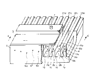
Referring to FIG. 1, an ink jet recording device in
accordance with the present invention is shown. As shown,
5 the device has a number of pressure chambers la, lb, lc, ld
and so forth (collectively 1). Side walls 2a, 2b, 2c, 2d and so
forth (collectively 2) delimit the pressure chambers 1 and are
formed of a piezoelectric material. Further, the pressure
chambers 1 are surrounded by a top plate 3, an under plate 4,
10 and a nozzle plate 5 which is positioned at one side of the
chambers 1. The nozzle plate 5 is formed with nozzles 6a, 6 b,
6c, 6d, 6e, 6f and so forth (collectively 6; 6a-6d are not
shown~. The nozzles 6 are each connected to the respective
pressure chamber 1. An ink pool 7 is communicated to the
15 rear portions of the pressure chambers 1. Electrodes 8a, 8b
and so forth (collectively 8) are respectively positioned on
the upper ends of the side walls 2 while electrodes 9a, 9b and
so forth (collectively 9) are respectively positioned on the
lower ends of the side walls 2. The electrodes 8 are
2 0 electrically connected to pads 10a, 10b, 10c, 10d and so forth
(collectively 10), respectively. The electrodes 9 are
electrically connected to a common electrode, not shown. The
pressure chambers 1, nozzles 6 and ink pool 7 is filled with
ink, not shown.
- 21874 ! 5
- 1 4-
The portions of the electrodes 8 and 9 facing the
pressure chambers 1 are covered with a protection layer, not
shown, so as not to contact the ink. The side walls 2 are each
polarized in the direction of its height, as indicated by
5 arrows P. The top plate 3 is flexible.
The above structural elements of the embodiment have
the following specific dimensions. The pressure chambers 1
have an inside width of 63.5 ,um each. The side walls 2 are
100 ,um high and 63.5 ~m wide each. The nozzle plate 5 is 80
1 0 ,um thick while the nozzles 6 have a diameter of 40 ,um each.
The length of each side wall 2 up to the ink pool 7 is 15 mm.
The under plate 4 has groove portions which are 100 ,um deep
each. Therefore, the pressure chambers 1 each h a s
dimensions of 63.5 ,um x 200 ,um x 15 mm. The nozzles 6 are
15 formed in the nozzle plate 5 at a pitch of 1 27 ,um .
The operation of the illustrative embodiment will be
described with reference to FIGS. 2A-2C which are sections
along line A-A' shown in FIG. 1. Assume that the pressure
chamber lb is driven to eject the ink via the associated
2 0 nozzle 6b, not shown, by way of example. To drive the
pressure chamber lb means to drive the piezoelectric s i de
walls 2b and 2c delimiting it. A voltage is applied to the side
walls 2b and 2c via the electrodes 8b and 9b and electrodes
8c and 9c, respectively. The voltage forms an electric field
2 5 in a direction indicated by an arrow E in FIG. 2B. Because the
- 1 5-
direction E of the electric field is coincident with the
direction of the polarization (direction P), the side walls 2b
and 2c expand in the direction E while contracting in the
direction perpendicular to the direction E, as shown in FIG. 2B.
5 As a result, the volume of the chamber lb increases an d
thereby lowers the pressure in the chamber lb. Therefore,
the ink is fed from the ink pool 7 into the chamber lb in the
same amount as the increase in the volume of the chamber 1 b.
Subsequently, the voltage is interrupted to cause the electric
1 0 field to disappear. Consequently, as shown in FIG. 2C, the side
walls 2b and 2c restore their original positions and again
reduce the volume of the chamber lb. This compresses the
ink in the chamber lb and ejects it via the nozzle 6b. Such an
operation is repeated at a preselected position at a print
1 5 timing with the print head shown in FIG. 1 being sequentially
moved relative to a sheet, not shown. As a result, a text
image or a graphic image is printed on the sheet in the form
of ink dots.
Conditions for driving the device shown in FIG. 1 will be
2 0 described on the basis of the results of experiments. FIG. 3
shows the waveform of a drive voltage. As shown, the drive
voltage applied to the side walls surrounding the the pressure
chamber to be driven is elevated to VO at a preselected rate,
then held at Vo for a preselected period of time, and t h e n
2 5 lowered to O V in a period of time to. FIG. 4 shows the results
2 1 ~74 1 ~
-1 ~
of experiments obtained when the period of time to an d
voltage VO were changed. When the voltage Vo w a s
sequentially increased with the period of time to maintained
constant, no ink drops were ejected so long as the voltage VO
5 was low. When the voltage exceeded a certain threshold Vt h,
ink drops began to be ejected. When the voltage Vo was
further increased above a certain value Vi f, ink drops began to
be ejected from the adjoining nozzle also. Let lines
connecting the points where Vt h and Vi f are obtained by
10 changing the period of time to be referred to as a critical
ejection line and a critical interference line, respectively.
Then, the range below the critical ejection line is a
non-ejection range while the range above the c r i t i c a 1
interference line is a range in which the ink is ejected even
1 5 from the adjoining nozzles. Therefore, the range above the
critical ejection line, but below the critical interference
line, is a stable ejection range. The pressure chamber is
driven in the stable ejection range. The critical interference
voltage Vi f iS substantially twice as high as the critical
2 0 ejection voltage Vth, as determined by experiments.
Therefore, the drive voltage Vo is selected to be above the
voltage Vt h, but below the voltage double the voltage Vt h
Presumably, the non-ejection range stems from the
surface tension of the ink existing in the nozzle; energy
2 5 overcoming the surface tension is necessary for the ink to be
21 ~741 5
- 1 7-
ejected. Why the range in which the ink is ejected even from
the adjoining nozzles is presumably as follows. Pressure
inside the pressure chamber next to the driven chamber
changes because one side wall thereof deforms. Such a
5 pressure change in the next chamber is considered to be about
one-half of the pressure change in the driven chamber.
Presumably, when the pressure change in the next chamber is
great enough to overcome the surface tension of the ink, ink
drops are ejected even from the adjoining nozzle.
1 0 The above is also true when the voltage is replaced with
the velocity of displacement of the piezoelectric side wall.
Assume that the critical velocity of displacement at which
ink drops begin to be ejected is Vt h. Then, the velocity of
displacement v allowing the ink drops to be stably ejected is
15 above Vt h, but below 2 x Vt h. The above condition may be
considered in terms of energy to be applied to the pressure
chamber, as follows. Assume that energy causing the ink
drops to begin to be ejected is Ut h. Then, energy U allowing
the ink drops to be stably ejected is above Ut h, but below
2 0 4 x Uth. It is to be noted that the critical values Vth, vth and
Uth depend on the physical property of the print head and that
of the ink and can be determined by experiments and/or
simulation.
In a first embodiment of the present invention, a
2 5 plurality of pressure chambers are driven so as to eject ink
21 8741 5
- 1 8-
drops via their nozzles. FIG. 5 is a timing chart
demonstrating the operation of the first embodiment. A s
shown, each pressure chamber 1 is driven at a period T and at
a time deviated from the next pressure chamber by T/3 or
5 2T/3. In FIG. 5, the pressure chambers la and ld are driven at
the same timing while the pressure chambers lb and le are
driven at the same timing. Likewise, the pressure chambers
lc and 1 f are driven at the same timing. That is, every third
chamber 1 is driven at the same timing. In this case, the
10 nozzles 6 of the nozzle plate 5 are arranged, as shown in
FIG. 6.
In FIG. 6, the nozzles 6a, 6b, 6c and so forth are
respectively communicated to the pressure chambers la, lb,
lc and so forth. Assume that the print head moves at a
15 velocity of Vh in the direction indicated by an arrow relative
to a sheet. Then, in FIG. 6, the nozzles 6a, 6d and 6g and t h e
nozzles 6b, 6e and 6h are deviated from each other by
d = vh T/3 in the direction of velocity Vh. Likewise, the
nozzles 6b, 6e and 6h and the nozzles 6c and 6f are deviated
2 0 by d = vh-T/3 in the above direction. Every third nozzle 6 is
arranged at the same leveI. When the pressure chambers 1 a r e
driven at the timing shown in FIG. 5 with the print head
having the nozzle arrangement of FIG. 6 being moved, ink
drops can deposit on virtual lattice points on a sheet. Use
2 5 may, of course, be made of a nozzle plate having every n-th
2187~15
1 9-
nozzle (n being 3 or greater natural number) arranged at the
same level, in which case every n-th pressure chamber will
be driven at the same timing.
A second embodiment of the present invention also
5 drives a plurality of pressure chambers so as to eject i n k
drops via their nozzles. This embodiment differs from the
first embodiment as to the drive timing and the positional
relation between the nozzles formed in the nozzle plate. As
shown in FIG. 7, the pressure chambers 1 are driven at a
1 0 period T. In FIG. 7, the chambers la, lb, le and lf are driven
at the same timing while the chambers lc and ld are driven
at the same timing. The chambers lc and ld and the chambers
la, lb, le and lf are deviated in timing by T/2 from each
other. The crux is that each two nearby chambers 1 are driven
15 at the same timing as each two nearby chambers 1 spaced
therefrom by two pressure chambers 1. FIG. 8 shows the
arrangement of nozzles 12 for practicing the above drive
scheme .
As shown in FIG. 8, nozzles 12a, 12b, 12c and so forth
2 0 are formed in a nozzle plate 11 and respectively
communicated to the pressure chambers la, lb, lc and so
forth. Assume that the print head moves at a rate vh in a
direction indicated by an arrow in FIG. 8. Then, the nozzles
12a, 12b, 12e and 12f and the nozzles 12c, 12d, 12g and 12h
2 5 are deviated from each other by e = vh-T/2 in the above
-- 21 8741 5
-2 O-
direction. Each two nearby nozzles are positioned at the s a m e
level as each two nearby nozzles spaced therefrom by two
nozzles. When the pressure chambers 1 are driven at the
timing shown in FIG. 7 with the print head having the nozzle
5 arrangement of FIG. 8 being moved, ink drops can deposit on
the virtual lattice points on a sheet. Use may, of course, be
made of a nozzle plate having every n-th nozzle (n being 3 or
greater natural number) arranged at the same level, in which
case every n-th pressure chambers will be driven at the same
1 0 timing.
A third embodiment of the present invention also drives
a plurality of pressure chambers so as to eject ink drops via
their nozzles. This embodiment differs from the first and
second embodiments as to the drive timing and the positional
1 5 relation between the nozzles formed in the nozzle plate. As
shown in FIG. 9, the pressure chambers 1 are driven at a
period T. In FIG. 9, the pressure chambers la and lb at driven
at the same timing while the pressure chambers lc and ld are
driven at the same time. Also, the pressure chambers le and
2 0 lf are driven at the same timing. The chambers la and lb and
the chambers lc and ld are deviated from each other by T/3.
Likewise, the chambers lc and ld and the chambers le and lf
are deviated from each other by T/3. Each two nearby
chambers 1 are driven at the same timing as each two
2 5 chambers 1 spaced therefrom by four chambers 1. FIG. 10
21 8741 5
shows nozzles formed in a nozzle plate 13 for practicing t h e
above drive scheme.
As shown in FIG. 10, nozzles 14a, 14b, 14c and so forth
formed in the nozzle plate 13 and respectively communicated
5 to the pressure chambers la, lb, lc and so forth. Assume
that the print head moves at a velocity vh in a direction
indicated by an arrow in FIG. 10. Then, the nozzles 14a, 14b,
14g and 14h and the nozzles 14c and 14d are deviated from
each other by d = vh-T/3 in the above direction. Likewise, the
1 0 nozzles 14c and 14d and the nozzles 14e and 14f are deviated
from each other by d = vh-T/3. Each two nearby nozzles are
positioned at the same as each two nozzles spaced therefrom
by four nozzles. When the pressure chambers 1 are driven a t
the timing shown in FIG. 9 with the print head having the
1 5 nozzle arrangement of FIG. 10 being moved, ink drops can
deposit on the virtual lattice points on a sheet. Use may, of
course, be made of a nozzle plate having every n-th nozzle
(n being 3 or greater natural number) arranged at the same
level, in which case every n-th pressure chamber will be
2 0 driven at the same timing.
While the illustrative embodiments each has a
particular drive timing and a particular nozzle arrangement,
in practice the individual pressure chamber is selectively
driven in response to a print command. Therefore, in each
2 S timing chart shown and described, each high level is
2187415
-2 2-
sometimes replaced with a low level. Of course, the
rectangular waves shown in the timing charts may b e
replaced with triangular waves, trapezoidal waves,
saw-toothed waves or any other suitable waves. In addition,
5 either of the positive logic or the negative logic may be used,
as desired.
Hereinafter will be described a control system for
controlling the ink jet recording device of the present
lnventlon .
1 0 In accordance with the present invention, to cause an
ink drop to be ejected from a certain nozzle, two
piezoelectric elements (side walls) defining the pressure
chamber communicated to the nozzle are driven, as stated
earlier. FIG. 11 schematically shows a specific control
15 system. As shown, print data 4 1 indicating whether or not to
eject an ink drop from the individual nozzle or representative
of information including an amount of ink drop are fed to a
data converter 42. The data converter 42 transforms the
nozzle-by-nozzle information to data meant for two
2 0 piezoelectric elements constituting the individual chamber.
Let the nozzles and piezoelectric elements each be provided
with serial numbers beginning with 1 (one). Then, when an i n k
drop is to be ejected from the nozzle #i, the data converter
42 transforms the input information to data for driving the
2 5 piezoelectric elements #i and #i+l. The data output from the
2187415
-2 3-
data converter 42 are fed to a controller 43. The controller
43 performs, e.g., pulse width modulation in accordance with
the element-by-element data, e.g., amount of an ink drop to be
ejected. The resulting print data output form the controller
43 are delivered to a driver 44. In response, the driver 44
selectively feeds power to the individual piezoelectric
elements of a print head 45 in accordance with the print data.
FIG. 12 shows a specific configuration of a circuit
included in the driver 44 and assigned to one of t h e
1 0 piezoelectric elements. The driver 44 is an assembly of such
circuits identical in number as the piezoelectric elements.
All the circuits of the driver 44 may share a single power
source V. At the time of printing, a print signal output fro m
the controller 43 is input to a buffer 46. In response, an
1 5 n-p-n transistor Ql causes its base voltage to go high with
the result that a base current flows and renders the
transistor Q 1 conductive. This causes the base voltage of a
p-n-p transistor Q2 to go low and causes a base current to
flow therethrough. As a result, the transistor Q2 turns on.
2 0 Consequently a current flows from the power source V to a
piezoelectric element C via the transistor Q2 and a serial
resistor Rs, raising the voltage of the element C and thereby
causing the element C to expand.
Subsequently, when the print signal output from the
2 5 controller 43 goes low, the base voltage of the transistor Ql
2187415
-2 4-
goes low and shuts off the base current, thereby rendering the
transistor Ql nonconductive. In response, the base voltage of
the transistor Q2 goes high and shuts off the base current,
thereby turning off the transistor Q2. As a result, the charge
5 stored in the piezoelectric element C is discharged via a
parallel resistor Rp parallel to the element C. The resulting
fall of the voltage of the element C causes the element to
restore its original position. Consequently, the element C
compresses the ink in the pressure chamber and thereby
1 0 ejects an ink drop. The driver 44 is therefore a CR
charge/discharge circuit which charges the element via the
resistor Rs and discharges it via the resistor Rp.
It has been customary with a drive circuit for the above
application to use an exclusive transistor or similar
1 5 switching device for each of charging and discharging. The
driver of the present invention is simple and inexpensive
because it does not need a switching element for discharging.
While in FIG. 12 the switching device is implemented as
a bipolar transistor, it may be replaced with an FET (Field
2 0 Effect Transistor), thyristor or any other suitable switching
device. The serial resistor Rs and parallel resistor Rp each
plays the role of resistance generating means. If desired,
such resistance generating means may be implemented by the
inside resistance between the power source and the
2~74~5
-2 5-
piezoelectric element or the inside resistance of the
piezoelectric element itself.
In accordance with the present invention, the diameter
of a dot to be printed on a sheet is variable, as follows. To
5 change the dot diameter, the amount of an ink drop to be
ejected may be changed. This can be done with the circuit of
FIG. 12 if the pulse width of the print signal is varied within
a range smaller than the time constant assigned to charging.
That is, the pulse width is reduced to eject a small drop or
10 increased to eject a large drop. Specifically, when the p u l s e
width is small, the voltage and therefore the displacement of
the piezoelectric element is reduced to, in turn, reduce the
variation of the volume of the pressure chamber, so that the
amount of a drop is reduced. When the pulse width is great,
15 the amount of a drop is increased.
FIG. 13 shows another specific control system c ap ab 1 e
of controlling the amount of an ink drop. The operation of t h i s
control system will be described with reference also made to
voltage waveforms shown in FIG. 14. As shown, the print data
2 0 41 indicative of an amount of an ink drop nozzle by nozzle are
input to the data converter 42. The data converter 42
transforms the nozzle-by-nozzle data to data meant for each
two piezoelectric elements forming a pressure chamber.
Again, let the nozzles and piezoelectric elements each be
2 5 provided with serial numbers beginning with 1. Then, when an
21 ~74 1 5
-2 ~
ink drop is to be ejected from the nozzle #i, the data
converter 42 transforms the input information to data for
driving the piezoelectric elements #i and #i+ 1.
The data output from the data converter 42 are input to
S a controller 53. In response, as represented by a waveform
(A) in FIG. 4, the controller 53 generates a first pulse Pl and
a second pulse P2 for a single print timing. The first pulse P 1
goes high at a time tl s and goes low at a time tle while the
second pulse P2 goes high at a time t2S and goes now at a time
1 0 t2e. The times tlS and t2e are constant for a single print
timing. The times tl e and t2S, i.e., the interval tb between the
two pulses Pl and P2 (tb = t2 S ~ tl e) is varied in accordance
with the amount of an ink drop. This successfully controls
the amount of an ink drop to be ejected.
As represented by a waveform (B) in FIG. 14, a waveform
generator 55 generates a voltage waveform resembling a
saw-toothed wave at a preselected period T. The waveform
(B) includes a rising portion and a falling portion. The
waveform (B) is input to a switching circuit 54. T h e
2 0 switching circuit 54 turns on and turns off the output voltage
of the waveform generator 55 on receiving the control pulse
Tl from the controller 53. As a result, the output voltage of
the waveform generator 55 is continuously applied to the
piezoelectric element of the print head 45 while the first and
2 5 second pulses Pl and P2 are in their high levels. Because the
21~74~5
piezoelectric element is a capacity element, the voltage
applied at the time tl e is substantially maintained even
during the interval between the times tl e and t2 s~ although
some voltage drop occurs due to natural discharge. The time
5 t 2 s when the pulse P2 goes high is unconditionally determined
by the voltage waveform output from the waveform generator
55 and the time tl e at which the pulse Pl ends. S tated
another way, at the time t 2 s, the voltage output from the
waveform generator 55 falls to a voltage equal to the voltage
1 0 at the time tle. Assuming that the saw-tooth wave rises over
a period of time of tl and falls over a period of time of t2,
then the interval tb between the pulses Pl and P2 is
expressed as:
tb = tl + t2 - (1 + t2/ tl) x ta Eq. (1)
Consequently, the voltage applied to the piezoelectric
element of the print head 45 has a waveform (C) shown in
FIG. 14. To change the amount of an ink drop, an arrangement
2 0 is made such that the pulse width ta of the pulse Pl is varied
while the interval t b between the pulses P 1 and P2 is
determined by the pulse width ta. To eject a large ink drop,
the pulse with t a is increased. As a result, the waveform (C)
rises and falls as represented by the second high voltage, so
- 21~7415
-2 8-
that a high voltage is applied to the piezoelectric element to
form a large ink drop.
With the above arrangement, it is possible to change the
voltage while maintaining its rate of fall constant, i.e., to
5 change the displacement of the piezoelectric element while
maintaining its rate constant. Consequently, the amount of an
ink drop can be changed without changing the velocity of the
ink drop.
It may occur that the velocity of an ink drop is not
10 constant, depending on the structure and configuration of t h e
print head and the property of the ink. In such a case, the
waveform output from the waveform generator 55 may be
modified, as shown in FIG. 15 by way of example. With t h e
waveform of FIG. 15, it is possible to vary the amount of an
1 5 ink drop while maintaining the velocity thereof constant.
Again, the voltage of the waveform generator 55 drops, at the
time t2s, to a voltage equal to the voltage at the time tl e. In
this manner, by matching the output waveform of the
waveform generator 55 to the characteristic of the print
2 0 head, the control system readily controls the amount of an ink
drop while maintaining the ejection velocity constant.
A reference will be made to FIGS. 16 and 17 for
describing a specific procedure for producing the ink jet
recording device shown in FIG. 1. As shown in FIG. 16, the
2 5 procedure is generally made up of the formation of
~ ~14~ ~
-2 9-
electrodes, the formation of pressure chambers, the
formation of a protection layer, and mounting.
First, the formation of electrodes begins with a step (A)
shown in FIG. 7. In the step (A), a 100 ,um thick piezoelectric
5 plate 2 is prepared which is formed of tricomponent type soft
ceramics produced by adding a perovskite type composite
oxide to PZT. 0.5 ,um thick films of tantalum are formed on
opposite major surfaces of the piezoelectric plate 2 by
sputtering in order to form the electrode 8 and and electrode
1 0 9. Subsequently, in a step (B), a pad 10 is formed on the edges
of the upper surface of the plate 2 by plating them with gold.
To form the pressure chambers, in a step (C) shown in
FIG. 17, a 300 ,um thick under plate 4 formed of the same
material as the piezoelectric plate 2 is affixed to the plate 2
1 5 by adhesive based on epoxy resin. Then, in a step (D), a
plurality of grooves each being 63.5 ,um wide are formed b y
cutting at a pitch of 127 llm. Each groove consists of a first
portion as deep as 200 ,um for playing the role of a pressure
chamber, and a second portion as shallow as 10 ~lm. This
2 0 shallow portion separates the electrode 8 and pad 10 in order
to form the electrode 8a, 8b, 8c and so forth and pad portion
lOa, lOb, lOc and so forth. The underside of the piezoelectric
plate 2 constitutes the common electrode 9.
To form a protection layer, the above laminate i s
2 5 immersed in a 0.1 % aqueous solution of phosphoric acid.
21 ~741 ~
-3 0-
Then, a voltage of 150 V is applied to the laminate with the
electrode portions 8 and common electrode 9 serving as an
anode. In this condition, the surfaces of the electrode
portions 8 and the portions of the common electrode 9
5 exposed to the pressure chambers are subjected to anodic
oxidation, so that they are covered with a 0.3 ,um thick oxide
film on anode of tantalum pentaoxide. At this instant, the
thickness of tantalum not subjected to anodic oxidation is
0.3 ,um .
1 0 The nozzle plate 5 is formed of polyimide and 80 ,um
thick. The nozzles 6 are formed in the nozzle plate 5 at a
pitch of 127 ,um by excimer laser, and each has a diameter of
40 ,um. In a step (E) shown in FIG. 17, the nozzle plate 5 is
adhered to the flush ends of the piezoelectric plate 2 and
15 under plate 4 by adhesive based on epoxy resin such that the
nozzles 6 respectively communicate to the grooves formed in
the plates 2 and 4. Then, in a step (F), the top plate 3 and ink
pool 7 are adhered to the top of the piezoelectric plate 2 by
adhesive based on epoxy resin such that they cover the above
2 0 grooves. The top plate 3 is formed of polyimide while the ink
plate 7 is formed of PES (polyether sulphone).
Subsequently, in a step (G) shown in FIG. 17, a printed
circuit board 15 is adhered to the underside of the under plate
4. Lead terminals 16a, 16b, 16c and so forth (collectively 16)
2 5 forth are formed on the printed circuit board 15 for
21&7~15
-3 1-
connecting the pad portions 10 and common electrode 9. The
lead terminals 16 are electrically connected to a driver, not
shown. The pad portions 10 and lead terminals 16 are
connected together by wire bonding. For this purpose, bonding
5 wire 17 made of gold is used. Further, in a step (H), the
common electrode 9 and lead terminals 16 are connected
together by conductive paste 18. The end of the ink pool 7
contacting the electrodes 8, the portions connected by
bonding and the portions to which the conductive paste is
10 applied are sealed by epoxy resin, although not s h o w n
specifically.
A second embodiment of the ink jet recording device in
accordance with the present invention will be descried with
reference to FIG. 18. This embodiment is identical with the
15 first embodiment as to the basic construction, basic
dimensions and operation of the print head as well as the
conditions and method of driving it. As for the fabrication,
this embodiment includes unique steps for the formation of
electrodes and pressure chambers. The following description
2 0 will concentrate on the differences between the first and
second embodiments.
First, the electrodes 8 and 9 are formed on opposite
major surfaces of the piezoelectric body 2, as in the first
embodiment. In a step (A) shown in FIG. 18, the upper
2 5 tantalum layer is etched in a preselected pattern by
21 &741 5
-3 2-
photolithography in order to form the electrodes 8a, 8b, 8c
and so forth. In a step (B), the end portions of the electrodes,
collectively 8, are plated with gold so as to form the pad
portions 10 (lOa, lOb, lOc and so forth). The bottom of the
5 piezoelectric plate 2 constitutes the common electrode.
A step (C) shown in FIG. 18 is identical with the step (C)
shown in FIG. 17. In a step (D), a plurality of 63.5 ~m wide
grooves are formed over a predetermined length at a pitch of
127 ~um. Each groove has a portion as deep as 200 ,um over a
1 0 preselected length. This portion plays the role of a pressure
chamber. Steps (E) through (H) shown in FIG. 18 are
respectively identical with the steps (E) through (H) shown in
FIG. 17.
FIG. 19 shows a third embodiment of the present
15 invention which is also identical with the first embodiment
as to the basic construction, basic dimensions and operation
of the print head as well as the conditions and method of
driving it. This embodiment differs from the first
embodiment as to the procedure for forming the pressure
2 0 chambers and the mounting procedure.
First, in steps (A) and (B) shown in FIG. 19, the
electrodes 8 and 9 are formed in exactly the same manner as
in the first embodiment. In a step (C) for forming the
pressure chambers, the under plate 4 is 300 llm thick and
2 5 formed of the same material as the piezoelectric plate 4. The
21874~5
under plate 4 is adhered to the piezoelectric plate 2 by
adhesive based on epoxy resin. In the illustrative
embodiment, a 0.5 ~lm thick tantalum film is formed on the
end of the under plate 4 by sputtering to serve as an electrode
5 19. The electrode 9 on the bottom of the piezoelectric body 2
and the electrode 19 are electrically connected by conductive
adhesive 20. Subsequently, in a step (D) shown in FIG. 19, a
plurality of grooves are formed in the piezoelectric plate 2 by
cutting at a pitch of 127 ~lm over the entire length of the
1 0 plate 2. The grooves are 63.5,um wide and 200 ,um deep each.
As a result, the electrode 8 and pad 10 are separated from
each other to form the electrodes 8a, 8b, 8c and so forth and
pad portions lOa, lOb, lOc and so forth.
A protection layer is formed in the same manner as in
15 the first embodiment. In a step (E) shown in FIG. 1 9, an end
plate 21 is adhered to the laminate by adhesive based on
epoxy resin in such a manner as to block the rear ends of the
grooves. Subsequently, in a step (F), the 80 ~lm thick nozzle
plate 5 formed of polyimide is adhered to the end of the under
2 0 plate 4 by adhesive based on epoxy resin. The nozzles 6 are
formed in the nozzle plate S at a pitch of 127 ~lm by excimer
laser, and each has a diameter of 40 llm. In the above step (F),
the nozzles 6 are respectively brought into communication
with the grooves formed in the piezoelectric plate 2 and
2 5 under plate 4. The top plate formed of polyimide and the ink
21~7415
-3 4-
pool 7 formed of PES are adhered to the top of the plate 2 by
adhesive based on epoxy resin in such a manner as to cover
the grooves of the plate 2.
Thereafter, in a step (G) shown in FIG. 19, the printed
5 circuit board 15 is adhered to the bottom of the under plate 4.
The circuit board 15 includes the lead terminals 16a, 16b,
16c and so forth for connecting the pad portions lOa, lOb, 1 0 c
and so forth and common electrode 19. The circuit board 15
is electrically connected to a driver, not shown. The pad
10 portions lOa, lOb, lOc and so forth and lead terminals 16a,
1 6b, 1 6c and so forth are connected by the bonding wires 17
formed of gold. The common electrode 19 is connected to the
lead terminals by the conductive paste 18. The portion of
each groove extending from the end of the ink pool 7 to the
1 5 end plate 21 is filled with epoxy resin, not shown. Further,
the bonded portions and the portions applied with the
conductive paste are sealed by epoxy resin, although not
shown specifically.
FIGS. 20, 21 and 22 respectively show a fourth, a fifth
2 0 and a sixth embodiment of the present invention. These
embodiments are respectively identical with the first, second
and third embodiments as to the basic construction, basic
dimensions and operation of the print head as well as the
conditions and method for driving it. As shown in each of
2 5 FIGS. 20-22, in the illustrative embodiments, the under plate
21874i5
-3 S-
4 has a greater size than the piezoelectric plate 2. A common
electrode 22 is formed on the upper surface of the under plate
4. The common electrode 22 is connected to the lead
terminals of the printed circuit board 15 by wire bonding.
FIG. 23 shows a seventh embodiment of the present
invention. This embodiment is identical with the f i r s t
embodiment in the basic construction, basic dimensions and
operation of the print head as well as the conditions and
method for driving it. The difference is that in this
1 0 embodiment the protection film formed by anodic oxidation
and covering the electrodes 8a, 8b, 8c and so forth and
electrodes 9a, 9b and 9c and so forth is replaced with a
protection film 23. The protection film 23 protects such
electrodes from the ink, not shown, filling the pressure
chambers la, lb, lc and so forth. The protection film 23 is
formed by sputtering silicon nitride. The rest of the
procedure is the same as in the first embodiment.
Referring to FIG. 24, an eighth embodiment of the
present invention will be described. As shown, in the
2 0 illustrative embodiment, use is made of a laminate
piezoelectric plate 24. The piezoelectric plate 24 is
configured such that a plurality of electrodes 25 laminated
therein are alternately electrically connected to outside
electrodes 26 and 27. The plate 24 is 400 ~lm thick and made
2 5 up of twenty layers spaced 20 ,um from each other. In a step
21~7415
-3 6-
(B) shown in FIG. 24, a gold film is formed on the edges of the
outside electrode 26 in order to form the pad 10. To form the
pressure chambers, in a step (C), the under plate 4 is adhered
to the laminate piezoelectric plate 24 by adhesive based o n
5 epoxy resin. The under plate 4 is formed of a piezoelectric
material and 500 ,um thick. A 0.5 ,um thick tantalum film is
formed on the end of the under plate 4 beforehand by
sputtering tantalum, implementing the electrode 19. The
outside plate 27 on the end of the piezoelectric plate 24 and
1 0 the electrode 19 on the end of the under plate 4 are
electrically connected by the conductive adhesive 20.
Subsequently, in a step (D), a plurality of grooves are formed
in the piezoelectric plate 24 by cutting at a pitch of 127 ,um
over the entire length of the plate 24. The grooves are
1 5 63.5 ,um wide and 500 ~m deep each. As a result, the outside
electrode 26 and pad 10 are separated into electrodes 26a,
26b, 26c and so forth and pad portions lOa, lOb, lOc and so
forth, respectively.
Subsequently, a film of silicon nitride is formed by
2 0 sputtering as in the seventh embodiment. This is followed by
a mounting procedure. First, in a step (E) shown in FIG. 24,
the end plate 21 is adhered to the end of the above laminate
by adhesive based on epoxy resin in such a manner as to block
the rear ends of the grooves. Then, in a step (F), the nozzle
2 5 plate 5 is adhered to the flush ends of the piezoelectric plate
2187415
-3 7-
24 and under plate 4 by adhesive based on epoxy resin. The
nozzle plate 5 is formed of polyimide and 80 ,um thick while
the nozzles 6 formed in the plate 5 by excimer laser each has
a diameter of 40 ,um. In the above condition, the nozzles 6 are
5 respectively brought into communication with the grooves
formed in the piezoelectric plate 24 and under plate 4. The
top plate 3 formed of polyimide and the ink pool 7 formed of
PES are adhered to the top of the piezoelectric plate 24 by
adhesive based on epoxy resin, covering the grooves of the
10 plate 24.
Thereafter, in a step (G) shown in FIG. 24, the printed
circuit board 15 is adhered to the bottom of the under plate 4.
The circuit board 15 includes the lead terminals 16a, 16b,
16c and so forth for connecting the pad portions lOa, lOb, 1 0 c
1 5 and so forth and common electrode 19. The circuit board 15
is electrically connected to a driver, not shown. The pad
portions and lead terminals are connected by bonding wires
17 formed of gold. The common electrode 19 on the end of the
under plate 4 and the lead terminals are connected by the
2 0 conductive paste 18. The portion of each groove between the
end of the ink pool 7 and the end plate 21 is filled with epoxy
resin, not shown. The bonded portions and the portions
applied with the conductive paste are sealed by epoxy resin,
although not shown specifically.
2187~15
-3 8-
The eighth embodiment is identical with the first
embodiment as to the operation of the print head and the
method of driving it. In the eighth embodiment, the portions
serving as the pressure chambers are each sized 63.5 ,um,
5 500 ~m x 4 mm. A typical drive voltage in the stable
discharge range available with the eighth embodiment is as
low as 15 V.
FIG. 25 shows a ninth embodiment of the present
invention. This embodiment is also identical with the f i r s t
1 0 embodiment as to the basic construction, basic dimensions
and operation of the print head as well as the conditions and
method for driving it. In the illustrative embodiment, a top
plate 28 is partly thinned to form an ink pool 29. The top
plate 28 is formed of the same material as the piezoelectric
1 5 plate or PES or glass.
FIGS. 26 and 27 show a tenth embodiment of the present
invention. This embodiment is also identical with the f i r s t
embodiment as to the operation of the print head and the
method of driving it. In the illustrative embodiment, a top
2 0 plate 30 covers the upper surface of the piezoelectric plate 2.
An ink pool 33 is formed in a printed circuit board 31 and a n
under plate 32 by milling or similar machining or by laser.
When the under plate 32 is implemented as a silicon
substrate, the ink pool can be formed by the anisotropic
2 5 etching of silicon.
2187415
-3 9-
In summary, it will be seen that the present invention
provides an ink jet recording device and a method of producing
the same which have various unprecedented advantages, as
enumerated below.
S ( 1) Two electrodes for applying a voltage to the side
walls of a piezoelectric plate lie in the range of a pressure
chamber, so that an electric field is prevented from acting on
portions which do not contribute to the ejection of an ink
drop. This obviates the waste of voltage and thereby realizes
1 0 low voltage drive which reducing the size of the pressure
chamber. All the grooves serve as pressure chambers without
any slit or similar wasteful space intervening between them.
This implements a multinozzle print head having a dense
configuration. With such a print head, the recording device
1 5 achieves a miniature and compact arrangement.
(2) A drive voltage is selected to be higher than a
critical ejection voltage, but lower than a voltage twice a s
high as the critical voltage. Alternatively, the displacement
velocity of the piezoelectric element is selected to be higher
2 0 than a critical ejection displacement velocity, but lower than
a rate twice as high as the critical velocity, or energy to be
applied is selected to be higher than a critical ejection
energy, but lower than energy four times as high as the
critical energy. This successfully obviates the interference
2 5 of the drive voltage, displacement velocity or energy with
21~7415
-4 O-
nozzles adjoining a target nozzle. It follows that a power
source of single polarity suffices and simplifies the
construction and reduces the cost.
(3) The electric field is formed in the same direction as
5 the polarization, so that an intense electric field can be
formed without any reversal of the polarization. Therefore, a
great displacement is achievable which reduces the required
volume of each pressure chamber. The device is therefore
dense, miniature and operable at high speed.
1 0 (4) A driver included in a specific control system has a
resistor electrically parallel to the piezoelectric element.
This eliminates the need for a switching device for
discharging and thereby simplifies the circuit arrangement.
(5) In another specific control system, while a
1 5 waveform generator outputs a voltage waveform having a
rising portion and a falling portion, a switching circuit feeds
it to the piezoelectric element by turning it on and off. A
first and a second pulse are respectively output when the
above voltage waveform rises and falls. The second pulse is~
2 0 generated when the output voltage of the waveform generator
falls to a voltage equal to the voltage appearing when t h e
first pulse goes low. The interval between the negative-going
edge of the first pulse and the positive-going edge of the
second pulse is controlled so as to control the amount of an
2 5 ink drop to be ejected. The amount of an ink drop is variable
2 1 874 1 5
-4 1-
while maintaining the velocity of the drop constant, if the
output waveform of the waveform generator is matched to t h e
characteristic of the print head and that of the ink.
(6) Because the direction of the electric field and that
5 of polarization are coincident, polarization can be done only i f
a voltage is applied via electrodes formed on the opposite
ends of the side walls of the piezoelectric body after the
print head has been completed. This realizes a simple and
cost-saving production procedure.
1 0 (7) Because polarization does not have to be effected
beforehand, adhesion, CVD, sputtering and other high-
temperature processes are applicable. Therefore, there can
be used a production method and materials which are reliable
and inexpensive.
1 5 (8) To form the pressure chambers, a flat top plate i s
simply adhered to the top of the piezoelectric plate formed
with a plurality of grooves. It is, therefore, not necessary to
accurately position the apexes of grooves and then join them
together. This further reduces the production cost an d
2 0 enhances stable production.
(9) An oxide film on anode for protection simplifies the
facilities, reduces the cost, and is extremely delicate and
reliable.
Various modifications will become possible for those
2 5 skilled in the art after receiving the teachings of the present
-- 21 8741 5
-4 2-
disclosure without departing from the scope thereof. For
example, in the first to sixth embodiments, the electrodes
may be formed by the sputtering, CVD or vapor deposition of
aluminum, titanium magnesium, niobium or zirconium. In t h e
5 seventh and eighth embodiments, the electrodes may be
formed by the baking, plating, vapor deposition, sputtering or
CVD of silver, silver palladium, platinum, nickel, gold or
nichrome or alloy thereof. In the seventh and eighth
embodiments, the protection layer may be formed by the
10 sputtering, CVD or dipping of sio2, Si3N4, BPSG, polyimide or
high molecule material. In the third, sixth and eighth
embodiments, the grooves may be formed not only by a cutting
saw but also by a wire saw or laser assisted etching or
similar chemical reaction.
1 5 Further, in all the embodiments shown and described,
the pad may be formed by the plating or sputtering of gold,
nickel or aluminum. For the under plate, use may be made of
PZT, alumina ~Al203), Si3N4, SiC, BN, ITO or similar ceramics,
glass (SiO2), Si, tantalum, aluminum, titanium, magnesium,
2 0 niobium, or zirconium. For the top plate, use made be made of
the same material as the piezoelectric plate forming the
pressure chambers, glass, ceramics or PES. In addition, the
nozzle plate may be formed of the same material as the
piezoelectric plate, glass, ceramics or nickel.
21874~5
-4 3-
While the nozzles have been shown and described as
being formed in the nozzle plate, they may alternatively be
formed in the top plate if desired.