Note: Descriptions are shown in the official language in which they were submitted.
w0 9s/28793 r~
2181452
-- 1 --
PWER ~lAllAl.~ "l FOR LINE POWERED TELECOMMUNICATION APPARATUS
~ he present invention relates to apparatus for
connoction to a communications line and more particularly,
~ but not exclusively, to power supply circuits for use with
line powered tolecommunication~ apparatus 'rhe invention
also relates to interrupt monitoring circuitG included in
8 uch apparatus .
~ elephones, particularly those with features such as
10 amplification, are known to draw line current ~or powering
from the telephone line. These circuits are only active when
a telephone is in the ~ off-hook" condition and do not usually
draw current when not in use.
Apparatus, such as facsimile transmission and
15 receiving apparatus or telephone answering machines, which
include monitoring circuits normally require relatively high
power and include battery or mains electricity power supply
8 ources .
As may be appreciated the ' A' and ' B' wires o~ a
20 telephone line in the c,uiescent state have a voltage
difference of approximately fifty volts d. c. in llnited
Ringdom telephone exchanges. ~his voltage is provided 80
that a telephone line circuit in the exchange can detect
looping o~ the line by a customer instrument by virtue of the
2~ current drawn. Such detection will occur if, say, a current
of twenty milliamps or greater is drawn, but 80me circuits,
particularly for longer lines, may be made more sensitive.
Thus if a telephone company wishes to provide line-
powered apparatus, for example for telemetry applications,
30 the current drawn from the telephone line must be less than
the loop detection at lower current limit. Purther, since
energy consumption is not without cost, if every telephone
line draws current in the ~uiescent state, such current draw
mus t be mi nimi 8 ed.
3~ Accordingly, the present invention seeks to provide
power supply circuits and interrupt monitoring circuits which
have minimal current draw in the c,uiescent state but which
W0 95/28793 ~ 9_
2~87452 ~ --
- 2 -
are capable o~ providing higher power when rec,uired.
According to the present invention there i8 provided
apparatus for ccnncction to a communications line including
,- ac to dc ccnverter connocted to receive power frcm line
5 t~rm' nl-l R, the ccnverter having a first lower power mode of
operation and a second higher power mode of operation, the
said converter powering a detector arranged for detecting the
presence of a predetermined activation signal on the
communications line characterised in that upon detection of
10 such a signal the converter is switched from the first mode
to the _econd mode to provide power to a second detector
which checks the validity of the activiation signal prior to
permitting the connection of power to other circuitE.
Preferably the dc to dc converter includes an
15 oscillator and a transformer, the oscillator being arranged
to cause dc level switching to a prim~ry winding of the
transformer such that power transfer from the communications
line to other circuits occurs, the change from the first mode
of operAt$on to the second mode being effected by causing an
20 incrcilse in the frequency of the oscillator.
An interrupt monitoring circuit including a power
supply circuit in accordance with the invention will now be
described by way o~ example only with reference to the
accompanying drawings of which:-
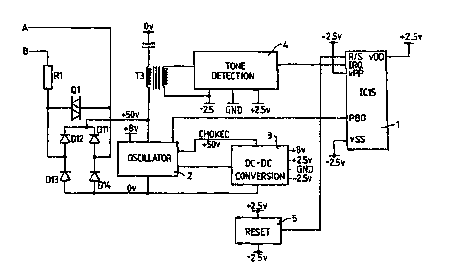
Figure 1 is a block schematic diagram of a part of a
telemetry monitoring apparatus;
Figure 2 i8 a circuit diagram o~ the oscillator of
Fi gure l;
Eigure 3 is a circuit diagram of the DC-DC converter
of Figure l;
Figure 4 is a circuit diagram o~ the tone monitoring
circuit of Figure l; and
Figure 5 is a circuit diagram of the reset circuit of
Fi gure l .
Referring ~irst to Figure 1, the telemetry monitoring
apparatus uses a ~I1U~J ~ microprocessor 1 to reRpond to
signals received over a telephone line (A, B). Most
,
~.
W0 9~/28793 2 ~ ~ 7 4 5 2 r~l ~
. --
connections of the microprocessor 1 are not shown slnce they
relate to functions which are not relevant to the present
invention.
In the quieacent state, that 18 when no telemetry
5 function i8 taking place, the microproceasor 1 remains in a
low power standby mode pending receipt of an interrupt signal
t i nput I RQ.
A tone detection circuit 4 monitors the telephone line
A,5 for a designated wake-up tone (or tones). Further detail
10 of the operation of the line detection circuit may be found
hereinafter.
The tone detection circuit 4 is supplied with power
from a DC to DC conversion circuit 3 switching for which is
provided by an oscillator circuit 2. All power for the
15 circuit 3 is drawn from the telephone line A, B by way of a
bridge rectifier circuit cm ~ ' ~ins diodes Dll - D14. The
bridgo circuit ensures that regardles8 of the polarity of tke
telephone exchange voltage on the A and B legs of the
telephone line plu8 fifty volt and zero volt lines are
20 consistent. The Diodes Dl 1-D14 may be of type IN4003.
A ten ohm resistor Rl prevents excess current being
drawn from the telephone line in the event of a short circuit
occurri ng.
Referring also to Figure 2, a ten henry inductance T1
25 prevents tones on the A and B legs being sunk by the
oscillator which compri8es an operational amplifier, IC4,
with both po8itive and negative feedback loops which vary the
frequency of output square wave. Once the oscillator circuit
4 is running, an 8 volt line is provided from the DC-DC
30 convertor 3. However, in order to start the power supply on
first connection the eight volt line is linked by a 47 k ohm
resistor R12 and a 39V zener diode DlS (type BZX8-539V) to
the fifty volt line. When the eight volt line is supplied
from the DC-DC converter 3 as hereinafter described, the
35 diode DlS thus limits current drawn direct from the plus SO
vol t 8 uppl y.
WO 95128793 A C 1~ .
21 87452
-- 4 --
The feedback loop of the Operatlonal Amplifier IC4
(which may be a MAX409BCPA manufactured by Maxim) comprises
a ten megohm resistor R23 linked to the positive input which
together with a further 10 megohm resistor R24 form a divider
5 which causes the positive input of IC4 to follow the square
w~ve outE~ut. The negative input of IC4 is linked to the
output by way of resistors R15 and R16 re8pectively of one
megohm and thirty three megohms. Capacitor C8 (ten
microfarad) allows the negative input to follow, charging
from the voltage divider chain formed from resistors R13, R14
each of 10 Megohm value between the ~8 volt and zero volt
lines.
Still con6idering the quie~cent st~te and referring
also to Figure 3, the square wave output of the oscillator 2
is fed by way of capacitors C3, C4 each of 680 picofarad
v~lue to switches Q2 and Q3. As the cJ~pacitor C3 is tied to
the ~50 volt line by 2 220R ohm resistor R10 and the
capacitor C4 to the zero volt line by corre8ponding resistor
Rll the output square wave (which was running at
approximately 200 I{z ) becomes a series of positive and
negative spikes of 100 micro second duratlon. Since
c~pacitor C11 (of 1 nanofarad) does not have time to charge
the output at the junction of the switches Q2 and Q3 switches
between zero and 50 volts.
Thus a transformer T2 which has one thousand turn
primPry winding and three secondary windings each of one
hundred ~nd sixty six turns is oau8ed to transfer power.
Although the input is spicate, ringing through the
tr~n8former will spread the transfer. A 100 n~n~f;!,rAA
30 A~co~rl i n~ capacitor C34 is provided to the plus 50 V line.
The first secondary winding feeds a full-wave
rectifier bridge circuit comprising four diodes D7, D8 and
D40, D41 which may be type 1~AX13 although a half-wave
rectifier may be used. A capacltor C14 ~ten microfar~ds)
35 smooths the output which provides a normal 8 volt supply to
the oscillator 2. As previously described, the eight volt
line biase8 the ~iode D15 (fig /) thus cau~ng power for the
W0 9~/28793
21 ~7~52
-- 5 --
oscillator to be drawn vla the trans~ormer T2 directly from
the telephone line A, B.
The other two windings for the transformer T2
effectively provide a centre-tapped five volt power supply.
5 A half-wave recti~ier circuit comprising diodes D9 and D10
provides plus 2. 5 v, Ground and -2. 5 V lines. While the
diodes D9 and D10 are type sAxl3, Diodes D26 and D23 are of
the zener type BZX2V7 to limit the output voltage.
Capacitors C12 and C13 provide smoothing of the output which
10 supplies power to the micLu~ essor 1 and tone detector 4 in
the quiescent state drawing approximately five microamps from
the line AB. For higher power applications it will be
realized that a full-wave recti~ier bridge muy be
incor,corated.
~f~rri n~ now to Figureg 1 and 4, the tone detoction
circuit 4 comprises an automatic gain control (AGC) circuit
6, a band-pass filter 7 and a signal level detector 8.
Incoming tone signals are transferred from the 50 volt
live side to the low voltage circuitry by a one to one
20 transformer T3. Such tone signals pass to the negative input
of an operational amplifier IC11 (which may be of type
~X409BCPA~, the signals being biased by a one megohm
resistor R2 connected to ground and a one hundred k ohm
resistor R3. A 470 n~nofAr:~ capacitor C31 completes the
25 circuit to the -2. 5 volt line while preventing dc flow
through R2.
Gain control is provlded by a feed back loop
c~ i n~ 100 k ohm regigtor R4 and a one megohm resistor RS
across which diodes D5, D6 (type BAX13) are provided. The
30 diodes DS, D6 will breakdown logarithmical if the output of
the operAtional ampli~ier IC11 exceeds approximately 0. 5
volts. By passing the resistor R5 thus increases the
feedback bias on the negative input o~ the operational
amplifier IC11 thus counteracting any high level output by
. 35 reducing amplification o~ the output feed.
The gain controlled signal now passes by way of a 1
megohm resistor R27 to the band pass filter 7 and more
WO 9~/28793 1 ~l,~.,
~87~3~ ~
-- 6 --
particularly to the negative input of the op amp IC12 which
again mAy be of type MAX 409BCPA). The filter comprising
capacitors C15, C16 and resistors R28, R29 feed back to the
input of IC12 and prevent all except a narrow band of signals
5 around the selected wake-up tone ~requency beins ~mplified
emd p~SSOa to the signal level detector 8.
In a specific example if the selected frequency (fO) is
493 Hz, ClS may be ten picofarad, C16 one microfarad and R28
and R29 each of one hundred k ohm.
Appropriate to fO signals pass by way of a 100
nnn~fnr~* capacitor C17 to the positive input o~ an op amp
IC13. 3i~sing o~ the input by one megohm resistor R31
connected to the ground line and ten megohm resistor R33
connected to the -2. 5 volt line to ensure that low level ~or
15 ~ccidental ) signals do not pass. A 8mall positlve feedback
by resistor R33 ~ten megohms ) and R32 ~2. 2 megohms ) provides
some hysteresis to the circuit.
An output line IR0 is normally birsed to ~2. 5 volts by
a ten megohm resistor R35. As the op amp IC13 converts an
20 incoming high level tone to a square wave, diode D18 is
forward bi~sed causing a falling edge to provide an interrupt
signal to the microprocessor 1.
ferri n5 again to Figure 1, the microproces80r 1 is
~rr~n~, on interrupt, to cause its output PB0 to go
25 neg~tive. This causes resistor R18 ~Figure 2) to dr~w
curront by way of a photon coupled bilateral field-effect
tran8istor IC5 and resistor R1~ thus reducing the resistor
feedback to the oscillator since IC5 now provides an
approximate two hundred ohm bypas8 o~ the resistor R16.
30 Capacitor C8 and re8istor chain R15, R16 causes the
oscillator output to approach a saw-tooth form. The positive
input of the op amp IC4 follows a low level square wave
provided by the resistors R23, R24 forming a divider and the
much faster rise time thus provided cause8 an increase in the
35 frequency of the osclllator 2. This increases the power
transferred by the transformer (T2 of Figure 3) t~mr~rArily
increasing the power drawn from the telephone line A, B.
,
WO 95128 793 ~
~ 2 1 87452
-- 7 --
ThiE temporary increase ln power available allows the
microprocessor IC15 to carry out an accurate frequency check
(approximately plus or minus one Xz) on the tone signal
output from IC13 to an input TCAP of the microprocessor. If
5 the tone is no longer present or i8 not of the required
value, the PB0 output i6 returned to normal and the
microprocessor returns to the quiescent state pending receipt
of a further interrupt via IRQ.
If the signal recoived is a valid "wake-up" signal
10 another output ~not shown) is used to cau~e a voltage supply
r~il for other circuits (also not shown) to be connected to
the -2. 5 volt supply by a transistor switch.
It is here noted that if power demand is maintained,
the frequency of the oscillator 2 will increase as capacitor
15 C7 discharges such that the input to the transformer T2
i~pproaches a high frequency square wave - having a period
which approaches the duration of the spike output of the
oscillator in the quiescent state.
For first connection or reconnection or in case the
20 occurrence of low or zero voltage for other reasons may have
caused the mi~ ,ylucessor 1 to enter an untenable state, a
reset circuit 5 (Figure 1 ) is responsive to rising voltage to
provide a reset signal. The reset signal (received at input
R15) will cause the mio~ .vc~lsor 1 to "re-boot" in known
25 manner.
Thus referring to Figure 5, an operational amplifier
IC7 is normally held switched off by biassing provided by
resistors R37 (10 megohm) R73 (5. 6 megohm) and R36 (4. 7
megohm). As the ~ and - 2. 5V line voltages increase from
30 zero, diode D25 conducts causing a change in the voltage on
the positive input pending re charging of capacitor C37.
This causes the output of IC7 to change which change shows as
a voltage edge passing thrcugh ClA causing the R/S bias
(provided by way of a 10 megohm resistor R41 ) to ch~nge.
35 This provides the reset signal to the microprocessor 1.
It will be appreciated that the single tone detection
circuit comprises of the filter 7 a~d level detector 8 ~ay be
_ _ _ _ _ , . _ . ... . , .. . _ _
WO gs/28793
~ ~ 87 ~52 ~
-- 8 --
moaificd to detect dual or multiple tone activation signals.
~hus, for ex~mple, for pTMF type signalling a second
~ppropriately tuned filter may be added at the output of the
AGC circuit 6.
While P8 herein descrlbed zener diodes have been u6ed
e~uivalent components of the type known as silicon stabilizer
diodes m~y ce used in plaoe thereof. The use of silicon
stabilized diodes in place of zener diodes has been shown to
~-o~ the pcv,r ~uu~wLlon o~ th~ it~