Note: Descriptions are shown in the official language in which they were submitted.
n v
n
- 1 -
BIAS SYSTEM IN AN OPTICAL CATV MODULATOR
The present invention relates to a method of carrying
out the analog modulation of an optical signal and to an
analog-external-modulation optical emitter.
The present invention also relates to a control system
for controlling the operating point or bias point of an
optical modulator used in CATV installations.
It is known that the distribution of television signals
by CATV (i.e. CAble Television) can be carried out not
only by means of coaxial-cable networks but also by the
use of optical fibres or of a mixed system (involving
fibres + coaxial cables).
The optical-signal modulation can be achieved either
directly (by intervention on the optical source, usually
a laser) or indirectly, by an optical modulator.
An indirect optical modulator enabling the amplitude
modulation to be carried out by a modulating signal
(also referred to as external signal) of very high
frequencies (as in the case of carriers for television
channels conventionally ranging from 40 to 860 MHz)
consists for example of a Mach-Zehnder type
interferometer built up on lithium niobate (LiNb03).
The electrooptical characteristic of modulators (optical
output power depending on the input radio-frequency
voltage) is typically non-linear. In order to limit the
signal distortion it is suitable for the modulator to
operate close to a portion of the characteristic which
is as linear as possible.
For the purpose, in an electrooptical modulator a radio-
- 2 -
frequency (RF) modulating signal is applied to a RF
electrode, and applied to the same electrode or to a
second bias electrode is a continuous bias voltage
determining the modulator bias point.
The modulating signal applied to the RF input for
example consists of the whole of the modulated carriers
of the television channels to be distributed to
subscribers.
In the case of a Mach-Zehnder modulator the course of
the characteristic can approach a sinusoid and it is
advantageous for the modulator to operate close to the
inflexion point of the sinusoid, at an applied bias
voltage VQ(bias point).
The modulation characteristic of the Mach-Zehnder
modulator, with reference to the bias point, can be
expressed by the relation:
Pu = KZ sen ~ (1)
wherein:
Pu is the optical output power
KZ is a coefficient depending on the Mach-Zehnder
modulator characteristic
~ - ~V/V~ is the modulation index of the modulated
signals, which index is expressed in radiants
V is the applied-voltage variation, with respect to
the bias point VQ
V~ is a constant.
This characteristic having a sinusoidal course is
identified by two values:
- the value of a voltage referred to as V~, representing
the voltage variation to apply to the RF (radio
frequency) electrode to bring the optical power from
the maximum value to the minimum value;
- the value of voltage VQ which is to be applied to the
bias electrode in order to make the bias point
2181596
_ 3 _
correspond to the inflection point of the
characteristic having a sinusoidal course, that is an
odd symmetry. In this case the even-order distortions
(comprising the second harmonic of the applied signals)
are cancelled and the odd-order distortions take a well
defined value.
For example, in the case of a Mach-Zehnder modulator of
the PIR PIM1510 type, manufactured by the Applicant,
said voltages can take the following values:
V~ - 4.3 V VQ - 0.7 V.
The VQ voltage value of the bias point is not constant,
but it varies in time (due to accumulation of static
charges in LiNb03, for example) and also with
temperature variations.
Therefore, the bias voltage value must be continuously
adjusted, for example using as information the presence
and quantity of the even-order distortions or the
second-order intermodulation products, generally
identified as CSO (Composite Second Order). The bias
point voltage must be applied and maintained by an
appropriate circuit.
Even in the case of operation of the modulator at the
bias point, the nonlinearity of the input-output
characteristic causes residual distortions, in
particular giving rise to intermodulation products of
the third order between the modulated signals generally
identified as CTB (Composite Triple Beat).
In order to restrict these distortions to some extent,
it is suitable that the selected modulation depth for
the modulating signals should not be too high (where by
modulation depth it is intended the maximum value,
expressed in percent, of the modulation index i3), a
modulation of about 4% per channel for example, in the
~~ ~l~'9~
- 4 -
case of the Mach-Zehnder modulator employed by the
Applicant, so that operation can take place as much as
possible close to the linear portion of the
characteristic.
In order to reduce residual distortions, and first of
all third-order distortions, the technique of
predistorting the modulating signals was suggested, so
that predistortion shall be compensated for by the
subsequent distortion on the part of the modulator; for
the purpose, it is possible to put a circuit, referred
to as linearizer circuit, ahead of the modulator, which
circuit has an input-output characteristic for the RF
signals which is the reverse function of the modulator
input-output characteristic.
This technique is for example disclosed in an article by
M. Nazarathy et al "Progress in Externally Modulated AM
CATV Transmission Systems", published in the Journal of
Lightwave Technology, vol. 11, No. 1, 01/93, pages 82-
104.
Therefore, after selecting an appropriate modulation
depth for the modulating signals, the modulator must be
equipped with appropriate circuits enabling
accomplishment of two functions:
a) applying the bias voltage and keep it to the required
value for making the modulator operate at the inflexion
point of the sinusoidal characteristic;
b) linearizing the modulator characteristic, by means of
predistortion circuits.
Together with the application of the bias voltage, it is
possible to apply a sinusoidal signal called "pilot
tone" of a predetermined amplitude and frequency (fl)
(generally much lower than the minimum frequency of the
RF signal band) and to detect, by an appropriate
circuit, the presence in the optical output signal of
2~~1~~~
- 5 -
the even harmonics of the pilot tone (the second
harmonic 2f1, for example). The bias voltage is such
adjusted that the value of this second harmonic is
minimized.
This technique, in order to enable an appropriate
stabilization of the bias point corresponding to CSO in
the order of 65-70 dB, needs a high modulation depth of
the pilot tone (about 10%, based on the experiments
carried out by the Applicant), so as to avoid
disturbances linked to noise, especially the intrinsic
photodiode noise.
A problem arising from this technique for stabilizing
the bias point is due to the fact that the presence of a
pilot tone, together with the modulating signals,
produces third-order beats which add up to the third-
order beats between the modulating signals, which are
in any case present due to the nonlinear (sinusoidal,
for example) modulator characteristic. In order to
restrict the quantity of such distortions it is
necessary, in contrast to what previously pointed out,
to keep the modulation depth of the pilot tone within
very low values (approximately 1%), which, as a result,
brings about the achievement of very low signal/noise
ratios for the feedback control signal of the bias
voltage stabilizing loop and therefore a weak efficiency
of the loop itself.
The selection of the pilot tone frequency and the
related modulation depth can be carried out by applying
several television channels to the modulator and looking
for the presence of possible disturbances (generally in
the form of transverse bars) on each of them, depending
on the width and frequency of the applied tones.
The Applicant has experimented that with a pilot tone
having a frequency fl of 10.7 MHz, the maximum width
2~~7~9~
- 6 -
applicable to the modulator (bias electrode) is about 12
mV, in order that the interference generated on the test
image of a television channel should not be visible.
This width corresponds to a modulation depth of about
1.20, which depth is inappropriate to achieve a good
signal/noise ratio.
In order to reduce the quantity of the intermodulation
products between the modulating RF signals (the
television carriers, for example), it is possible to
employ, as said, the linearization-by-distortion
technique.
This technique can be also used for the pilot tone of
the bias voltage control. In this case it is necessary
to send the pilot tone together with the RF signals,
that is they are to be sent to the input of the
modulator predistortion circuit. Thus, both beats
between the modulating signals and beats between the
signals themselves and the pilot tone are linearized.
The Applicant could see that this involves further
practical difficulties, in that the circuits amplifying
the signals before sending them to the modulator are
generally band-limited (they are for example limited to
the 40 - 860 MHz television band) externally of which
band it is impossible to obtain a satisfactory behaviour
(width and phase linearity), capable of compensating for
further third-order distortions introduced by the pilot
tones used to control the bias voltage.
According to the present invention these difficulties
are overcome by a new method enabling the use of
amplifiers with a band limited to the modulating signal
band (for example, with a 40 - 860 MHz band in the case
in which the modulating signals are the whole of the
carriers of television signals), without making it
necessary to use amplifiers of a wider band extended to
z~ s~~~~
the low frequencies so as to include the pilot tones,
which amplifiers are expensive and of difficult
accomplishment.
The present invention also enables the modulation depth
of the pilot tone to be increased up to 10% without
high-level third-order distortions being produced, and
therefore enables a high efficiency of the bias-voltage
stabilization loop to be achieved.
In one aspect, the present invention relates to a method
of analogically modulating an optical signal in
correspondence with a signal of a frequency within a
band of predetermined width, comprising:
- feeding an optical input signal to an electro-optical
modulator;
- feeding an external electric signal of a frequency
within said band to a linearizer circuit and
correspondingly generating at the output a predistorted
electric signal having a predistortion of predetermined
characteristics;
- feeding said predistorted electric signal to the input
of said electro-optical modulator;
- feeding an electric bias signal to the input of said
electro-optical modulator;
- generating an optical modulated signal in said
electro-optical modulator;
wherein said step of feeding an electric bias signal
comprises:
- generating an electric piloting signal (pilot tone) at
a predetermined frequency;
- generating an electric control signal in
correspondence with said modulated optical signal;
- generating an electric bias signal in correspondence
with said electric control signal, said pilot tone and
with a reference signal of predetermined voltage, in
combination with each other;
characterized in that it further comprises:
_ g _
- feeding said pilot tone in superposition with said
external electric signal to the input of said linearizer
circuit;
- attenuating said pilot tone at the output of said
linearizer circuit before feeding said predistorted
electric signal to said electro-optical modulator.
Preferably said predetermined frequency is external to
said band of predetermined width.
Preferably said step of generating an electric control
signal comprises separating a fraction of said modulated
optical signal and detecting an electric feedback signal
corresponding thereto and more preferably drawing the
component at said predetermined frequency from said
electric feedback signal.
In a particular embodiment, said method comprises the
steps of
- generating a first and a second electric piloting
signal (pilot tones), at a first and a second
predetermined frequencies, respectively;
- feeding said first and second pilot tones in
superposition with said external electric signal to the
input of said linearizer circuit;
- attenuating said first and second pilot tones at the
output of said linealizer circuit before feeding said
predistorted RF signal to said electrooptical modulator,
and wherein said step of generating an electric control
signal comprises drawing from said electric feedback
signal, the component at the frequency difference
between said first and second predetermined frequencies.
Preferably, said first and second predetermined
frequencies are external to said band of predetermined
width.
According to an advantageous version of this particular
2181~~~
- 9 -
embodiment, this method comprises:
- drawing from said electric loop signal, a second
component at the frequency difference between twice one
of said first and second predetermined frequencies and
the other of said first and second predetermined
frequencies;
- generating a linearization control signal based on
said second component;
- controlling said linealizer in a parametric manner,
based on said linearization control signal, so as to
minimize the third-order distortions of said modulated
optical signal.
In a further particular embodiment of said method, said
external electric signal comprises at least two spaced
apart frequencies in said band and said step of
generating a predistorted electric signal comprises
generating second-order and third-order intermodulation
products between said frequencies and pilot tone, of
such characteristics that they are superposed in
substantial phase opposition with the corresponding
intermodulation products generated within said
electrooptical modulator.
Preferably, said method comprises attenuating said pilot
tone by at least 10 dB at the output of said linealizer
circuit.
More preferably, said step of attenuating said pilot
tone at the output of said linearizer circuit comprises
filtering said pilot tone by a band-stop filter, or it
comprises adding, at the output of said linearizer
circuit, a signal obtained at said pilot tone, varying
the phase and width of same according to predetermined
quantities.
In a second aspect, the present invention relates to an
analog-external-modulation optical emitter comprising an
CA 02187596 2001-10-10
77909-61
optical source, an electro-optical modulator and a piloting
circuit of said electro-optical modulator, said electro-
optical modulator having: an optical input for an optical
signal, in connection with said optical source, a first
5 electric input for a modulating voltage, a second electric
input for a bias voltage, and an optical output carrying an
analog modulated optical signal, an optical coupler being
connected to said optical output of said modulator, which
optical coupler has a branch carrying one modulated-optical-
10 signal portion in connection with an optical receiver,
adapted to generate an optical control signal in
correspondence with said optical signal; in which said
piloting circuit comprises: an input for an analog external
electric signal, a linearizer circuit receiving said
external signal and connected to said first electric input
of said electro-optical modulator; an input for a
predetermined bias voltage; an input for said electric
control signal generated by said optical receiver; a circuit
generating an electric piloting tone signal; said
predetermined bias voltage and electric control signal being
fed to the input of a differential amplifier, the output of
said differential amplifier being combined with said
electric piloting circuit and the combination being fed to
said second electric input of said electro-optical
modulator; characterized in that the circuit generating an
electric piloting signal is also connected, via a band-pass
filter and an attenuator-phase shifter circuit, to the input
of said linearizer circuit and the output of said linearizer
circuit is then sent to said first electric input of said
electro-optical modulator by interposition of a band-stop
filter adapted to eliminate said electric
218759b
- 11 -
piloting signal downstream of said linearizer circuit.
More details will become apparent from the following
description, with reference to the accompanying
drawings, in which:
- Fig. 1 is a diagram of an analog-external-modulation
optical emitter;
- Fig. 2 is a graph of the experimental results obtained
in one embodiment of the present invention;
- Fig. 3 is a diagram of an analog-external-modulation
optical emitter employing two pilot tones;
- Fig. 4 is a diagram of an analog-external-modulation
optical emitter employing two pilot tones and provided
with a parametric control of the third-order
distortions.
An analog-external-modulation optical emitter according
to the present invention will be now illustrated with
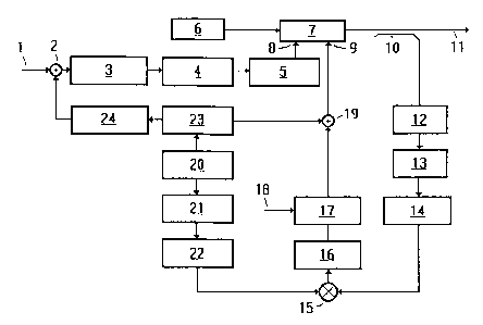
reference to the block diagram of Fig. 1.
An input for electric radio-frequency (RF) modulating
signals included within a given frequency band has been
identified by reference numeral 1. Input 1 is connected
to one of the inputs of a summation node 2, the output
of which is connected to a linearizer 3. This linearizer
is formed of a predistorter circuit, provided with one
input-output characteristic (output voltage depending on
the input voltage) selected as stated in the following.
Linearizer 3 is followed by a band-stop filter 4,
centered on the frequency of a pilot tone described
later, and an amplifier 5, operating in the frequency
band of the RF signals.
The output of amplifier 5 is connected to an electrode 8
of an electrooptical modulator 7. Electrode 8 is
arranged for the input of RF modulating signals.
A second electrode 9 of modulator 7 is arranged for the
2~ ~~'~96
- 12 -
input of a bias signal, by which the modulator bias
point is determined.
While the presence of two separate electrodes for the
modulating and bias signals is preferred to the ends of
the present invention, in place of the stated modulator
it is possible to employ an electrooptical modulator
provided with one control electrode alone, wherein the
modulating and bias signals are combined by means of an
appropriate circuit.
Connected to an optical input of modulator 7, by an
optical fibre for example, is a radiation source 6
capable of generating a continuous optical signal. This
source may consist of a laser, in particular of the
semiconductor type.
The optical modulator output is connected, by an optical
fibre for example, to an optical coupler 10 adapted to
separate the radiation coming from modulator 7 so as to
send part of same, preferably in the range of 80% to
99.5%, more preferably in the range of 90% to 99%, to an
optical output 11, and the remaining part to an optical
receiver 12 comprising a photodiode, for example.
The input-output characteristic of the linearizer 3 must
be selected based on the input-output characteristic of
the electrooptical modulator 7, so as to compensate for
the nonlinearity of the latter, or so as to obtain a
relation as much as possible linear between the power of
the optical signal coming out of the modulator and the
modulating signal voltage present at the input 1; in
particular it must be such selected as to minimize the
third-order distortions.
An electric RF signal, called pilot tone, of frequency
fl lower than the lower limit of the modulating signal
band, is generated by a generator 20.
~18759b
- 13 -
Connected to generator 20 is a band-pass filter 23,
centered on frequency fl and adapted to attenuate a
possible component at frequency 2f1 (second harmonic of
the pilot tone). Connected to the band-pass filter 23 is
an attenuator-phase shifter 24, in turn connected to a
second input of the summation node 2. Phase-shifting and
attenuation of the attenuator-phase shifter 24 can be
adjusted, as stated in the following.
The electric signal generated by receiver 12 in
correspondence with the optical signal from coupler 10
is sent to a band-pass filter 13, centered on frequency
2f1; connected to the output of the band-pass filter 13
is an amplifier 14, the output of which ends up in a
first input of an analog multiplier 15.
The analog multiplier 15 carries out the coherent
detection of the signal at frequency 2f1 coming from
receiver 12 through the band-pass filter 13 and
amplifier 14; thus a tone at the second harmonic of the
pilot tone and coming, via an adjustable phase shifter
22, from a frequency doubler 21 connected to generator
20, is sent to a second input of the analog multiplier
15.
The adjustable phase shifter 22 is such adjusted that it
optimizes the demodulation of the signal at frequency
2f1 coming from amplifier 14.
The analog multiplier 15 output is connected to the
low-pass filter 16 eliminating the high-frequency
components, so that at the output of same only the
continuous component corresponding to the detected
signal is present.
A reference bias signal 18 and the detected signal from
the low-pass filter 16 are respectively connected to the
- 14 -
two inputs of the differential amplifier 17.
The differential amplifier 17 output is connected to an
input of the summation node 19, in which the pilot tone
coming from the band-pass filter 13 and connected to a
second input of the summation node 19 is superposed with
the signal from the differential amplifier 17; the
output of the summation node is connected to the bias
electrode 9 of the electrooptical modulator 7.
The optical connections, as well as the electric
circuits relative to the operating blocks forming the
device of Fig. 1, can be made following known
techniques.
Operation of the device takes place as follows.
The bias voltage control is carried out by injecting a
known-frequency signal (not interfering with the
television channels) into the modulator 7 and detecting
the amplitude and sign of an even harmonic of this
signal, in particular of the second harmonic, since the
amplitude of same is greater than that of the harmonics
of a higher order.
The amplitude and sign of the second harmonic can be
emphasized by a synchronous detector comparing the
second harmonic present in the signal at the modulator 7
output (converted to an electric form by a photodiode),
with the second harmonic of the signal injected into the
modulator itself.
In particular, the signal of an oscillator 20 of
appropriate amplitude and frequency fl (generally below
the minimum frequency of the television channels equal
to about 40 MHz) is applied to the RF input port 9 of
the modulator. Supposing that the bias voltage is not
the optimal one, also the even harmonics (in addition to
2~$1~~9b
- 15 -
the odd harmonics) of the applied signal will be present
at the modulator output.
By an optical coupler 10 a fraction of the optical
output power is drawn from modulator 7 and it is sent to
the photodiode of the receiver 12 converting it into
an electric signal.
The signal is subsequently (13, 14) amplified in a
selective manner at the frequency of the second
harmonic. This signal is compared (amplitude and sign)
through the synchronous demodulator, with the signal
from oscillator 20, and frequency-doubled (21). An
analog multiplier 15 is used as the synchronous
demodulator.
The demodulator output consists of a continuous
component and a second-order beat of the signals
entering the analog multiplier 15, which beat is
eliminated by the low-pass filter 16.
The continuous-component value depends on the deviation
of the bias voltage from the optimal value, because it
depends on the amplitude and phase of the second
harmonic present at the modulator output.
It can be seen that the smaller the deviation of the
bias voltage from the optimal value, the greater the
attenuation of the composite second order (CSO).
In the device of the present invention, the problems
related to the stability and response of the bias
voltage-controlling loop (feed-back loop) can be solved
by an appropriate selection of the compensation pole,
after determining the overall loop response.
The device also provides that the pilot tone should be
sent to the linearizer 3 together with the modulating
2117596
signals. In this manner in the predistortion circuit
there is the generation of the signals compensating for
the distortions produced in the modulator by
superposition of the modulating signals with the pilot
tone applied to the modulator together with the bias
controlling voltage.
The pilot tone sent to the linearizer 3 must be such
that it can be suitably amplitude- and phase-varied, by
a variable attenuator-phase shifter, in order to obtain
the maximum elimination of the third-order beats between
the pilot tone and the modulating signals.
According to the present invention, only the
predistortion circuit 3 (and in particular the input
circuits thereof) must have an appropriate response to
the pilot tone frequency, whereas the amplifier does not
require such a response.
In order to avoid the pilot tone reaching the optical
modulator through the amplifier, it is possible to
introduce a band-stop filter 4 between the predistortion
circuit and the amplifier, so as to conveniently
attenuate (attenuation of at least 10-15 dB) the pilot
tone.
Alternatively, it is possible to efficiently attenuate
the pilot tone by adding, after the linearizer, the
pilot tone itself with opposite phase. In more detail,
in place of the band-stop filter 4, a summation node,
not shown in the figure, can be connected between the
predistorsion circuit 3 and the amplifier 5, in order
that a signal, obtained from the pilot tone by modifying
its phase and amplitude so to minimize the output
component at the pilot-tone frequency, is added to the
signal from the predistorsion circuit 3 by means of said
summation node.
This alternative solution has the advantage of modifying
- 17 -
the spectrum of the signal entering the amplifier only
at the exact frequency of the pilot tone.
Example
Still with reference to the block diagram of Fig. 1, an
example of a device according to the present invention
made by the Applicant will be now described.
The used electrooptical modulator is a Mach-Zehnder-type
modulator, model PIR PIM1510, produced by the Applicant.
The pilot tone is generated by a quartz oscillator 20 at
a frequency fl - 10.7 MHz. The frequency selection
essentially depends on practical reasons, since band-
pass filters at said frequency and also at a double
frequency (2f1 - 21.4 MHz), to be used in the circuits
following the optical receiver (photodiode) are easily
available on the market.
The tone at frequency fl = 10.7 MHz applied to the Mach-
Zehnder modulator 7 has a level such that a modulation
depth of about 10% is introduced.
The tone at frequency fl = 10.7 MHz is frequency-doubled
before being sent to the coherent detector consisting of
the analog multiplier 15, at which also the signal drawn
from the modulator 7 output arrives, by means of an
optical coupler 90%-10% picking up a 10% portion of the
optical output power.
After opto-electrical conversion carried out by the
photodiode, the signal is amplified and filtered at the
frequency 2f1 - 21.4 MHz. In addition to the second-
harmonic signal (2f1 - 21.4 MHz), the photodiode also
detects the fundamental frequency (fl = 10.7 MHz) having
an amplitude about 70 dB greater. Therefore, the
introduction of a filter eliminating the fundamental
frequency is necessary in order to avoid the subsequent
21 ~l ~~1~
- 18 -
circuits being overcharged, which will result in the
generation of a signal at the second-harmonic frequency,
before the synchronous detection, thereby altering
operation of same.
The phase of the signal with frequency of 21.4 MHz that
is inputted to the analog multiplier 15 can be adjusted
for optimizing demodulation, by means of the adjustable
phase shifter 22 following the frequency doubler 21. The
optimal adjustment is found by maximizing the
continuous-voltage variation at the synchronous
demodulator output for a given variation of the
modulator bias voltage VQ.
The voltage outputted from the analog multiplier 15 is
conveniently filtered by a low-pass filter 16 letting
only the continuous component pass and eliminating other
undesired signals. This voltage is compared, by the
differential amplifier 17, with the reference bias
voltage 18 and applied to the optical modulator 7,
together with the pilot tone.
The pilot tone injected into the linearizer 3 must be
conveniently filtered too, in order to avoid the
introduction of spurious tones with respect to the pilot
tone; in addition, it must be conveniently amplitude
and phase-adjusted (by an attenuator and a phase
shifter, respectively) so as to minimize the (third
order) intermodulation products generated around the
television carriers.
Amplifier 5 is a common CATV amplifying module operating
in the 40-860 MHz band, and more particularly model
CA922A, manufactured by Motorola.
It is pointed out that it is not necessary to resort to
amplifying modules operating at the pilot tone
frequency, in particular at frequencies down to less
- 19 -
than 10 MHz; this would require the use of input and
output transformers of difficult construction, because
an increase in the primary and secondary inductance of
the transformers, which increase would be necessary to
improve the response of said transformers towards low
frequencies, would bring about an increase in the stray
capacitances such as to reduce the high frequency
response down to values lower than 860 MHz, as required
for covering the whole UHF television band.
Experimental results related to the described example
are reproduced in the graphs of Fig. 2. The x-axis
corresponds to frequencies, whereas the RF spectra
expressed in dB, standardized with respect to the
considered carrier are reproduced along the y-axis.
For the experiment, used as the modulating signal was
the whole (with equalization of ~ 0.2 dB) of the 80
carriers corresponding to the NTSC television standard,
with frequencies included between 55.25 and 547.25 MHz.
In particular, curve A corresponds to the RF spectrum of
the television channel transmission carrier centered at
the frequency of 355.25 MHz.
Curves B and C, instead, reproduce the RF spectra
measured after quenching of the carrier at the frequency
of 355.25 MHz, in the presence of the remaining
carriers. The centre peak is due to the third-order
intermodulation between the remaining carriers. The side
peaks are instead due to the third-order intermodulation
between the remaining carriers and the pilot tone at the
frequency of 10.7 MHz.
In the depicted experimental configuration curve C was
achieved. Curve B was instead achieved in a
configuration otherwise identical with the preceding
one, in which connection between the attenuator-phase
218759
- 20 -
shifter 24 and the summation node 2 had been cut off so
as to stop input of the pilot tone into the linearizer
3.
One can see that in the device of the present invention
(curve C) the third-order intermodulation between the
carriers and pilot tone (CTB) has a value lower than
-75 dB whereas, in the device in which the pilot tone is
not injected into the linearizer (curve B), CTB < -62
dB.
The present invention enables a high modulation depth to
be adopted for the pilot tone, so as to avoid noise-
linked disturbances, above all the intrinsic photodiode
noise, while at the same time reducing the CTB between
the pilot tone and television carriers.
In particular, by sending the pilot tone together with
the television signals to the input of the modulator
predistortion circuit, both beats between the television
carriers and beats between the carriers and the pilot
tone are linearized.
In the device according to the present invention, as so
far described, minimization of the third-order
distortions due to beats between the television carriers
is achieved by means of the linearizer which is adjusted
in a constant and non parametric manner.
While a device making us of one pilot tone alone has
been described, a system according to the present
invention can be accomplished by using two pilot tones.
For the purpose it is possible to apply two pilot tones
of predetermined amplitude and frequency (fa, fb),
together with the bias voltage. In this manner, two
control signals can be obtained, one to minimize the
second-order distortions and one to minimize the third-
- 21 -
order distortions, for example utilizing the beats:
fa-fb (second order)
2fa-fb or 2fb-fa (third order) .
Frequencies fa and fb, too, are generally selected of a
much lower value than the frequencies of the RF
modulating signals (the television channels, for
example).
Fig. 3 shows a block diagram relative to a device
according to the present invention employing two pilot
tones. In Fig. 2, components that are analogous to those
in the device of Fig. 1 have been allocated the same
reference numerals.
In Fig. 3 denoted by 30 is a two-pilot-tone generator
with predetermined frequencies fa and fb and by 31 a non
linear device connected to the preceding generator and
capable of producing a signal at the beat frequency fa
fb, starting from the pilot tones.
Denoted by 33 is a filter capable of transmitting the
pilot tone frequencies and attenuating the other
frequencies; 34 identifies a band-stop filter adapted to
attenuate the two pilot tone frequencies. 32 is a band-
pass filter centered on frequency fa-fb.
The device of Fig. 3 enables the bias point of modulator
7 to be stabilized, by minimizing the beat at frequency
fa-fb in the optical receiver 12. The device, like that
of Fig. 1, also enables the third-order beats between
the television carriers and the two pilot tones to be
reduced.
In addition, this device enables the signal/noise ratio
for the feedback signal of the bias voltage stabilizing
loop to be improved, the modulation depth of the pilot
tone remaining unchanged. In fact, beat at frequency fa-
218759
- 22 -
fb is more intense, for an equivalent displacement with
respect to the bias point, than the corresponding signal
at the second harmonic of the pilot tone that would be
measured in the device using a single pilot tone.
The device of the present invention as shown in the
block diagram of Fig. 4, in addition to enabling the
bias voltage control, also allows the third-order
intermodulation products to be controlled, by acting on
the linearization circuit. In this way a parametric
adjustment of both second order and third order
intermodulation products is achieved.
In Fig. 4, components that are analogous to those of the
device of Fig. 3 have been allocated the same reference
numerals.
Denoted by 41 is a non-linear device connected to the
pilot tone generator 30 capable of producing a signal at
the beat frequency 2fa-fb, starting from the pilot
tones; 42 identifies an adjustable phase shifter, 43 an
analog multiplier and 44 a low-pass filter connected to
an amplifier. Component 44 lets the continuous component
pass and eliminates the second-order beat of the signals
entering the analog multiplier 43.
Components 41, 42, 43, 44 altogether form a synchronous
demodulator of the signal at frequency 2fa-fb coming
from the optical receiver 12 through filter 45, that
behaves as band-pass at the same frequency, and
amplifier 46.
This signal at frequency 2fa-fb, linked to the third-
order beats, is used after demodulation to control a
parametric linearizer 47 connected to the output of
filter-amplifier 44.
The feedback loop comprising filter 45, analog
2187596
- 23 -
multiplier 43 and parametric linearizer 47 enables the
CTB of the device to be conveniently minimized, under
variation of the non-linearity parameters of the
modulator 7 and of any other optical or electronic
component, in the path of the modulating signal, being
comprised between the linearizer 3 and optical receiver
12.
Circuit examples of the bias-voltage control systems
employing two pilot tones, corresponding to the devices
of Figs. 3 and 4, can be made, in whole similarity with
the example described in connection with the case of a
single pilot tone, by applying two pilot tones at the
frequencies of 33.4 MHz and 38.9 MHz and employing known
techniques for making the additional components.