Note: Descriptions are shown in the official language in which they were submitted.
wos~l3o3l9 21 8761 ~ r~"~ r~73
Ti-- switch sYstem.
Technical area.
Generally, the invention relates to a switch system in
which circuit switching is performed in a distributed time
switch in which time switching units are located in switch
ports connected to a time shared medium in a switch core.
More particularly, the present invention relates to a
digital time switch system which inc~llrl~c a switch core and a
number of switch ports and is intended to be used in a
tele~ ication network, in which the switch ports share
the bandwidth of a bus by time-division multiplexing, on
which the time is divided into time slots which are A'~ lecl
in frames, data transmission between the switch ports is
performed in time slots which have been ~iqned to a
respective switch port by a superior control means so as to
avoid bus conflict, and each switch port has access to the
whole bandwidth of the bus and by means of the superior
control means selects the data which is intended for the
switch port.
S~An-l Of th~ Art.
In switch systems wherein the switch core consists of a
common time shared medium the switch core can be very simple.
In known systems of this kind the switch core often consists
of only a passive bus.
One advantage of switch systems of this type is that the
costs of the switch core become low, whereby higher cost
modularity can be attained for scAl~Ahle systems. Since the
switch core constitutes ~ fixed basic cost for a system, the
total cost f or small systems can be lower when the cost of
the switch core is low, whereby the cost efficiency becomes
better for these small systems.
A passive bus can, however, suffer from several problems.
35 One problem is that ~:,L-,euusly appearing switch ports can
disturb the function of the bus by driving it at points of
time which have been Acsiqn~d to other switch ports. This can
W095130319 21876la ~ 173
result in bus conf lict.
Another problem is the high ~ u~.l. y properties of the
bus. More particularly, at high ~ ue..cies ; ~ nre
adaption is required, since the bus then has the character of
a tri~n~ sirn line. For different reasons the bus is,
however, difficult to; ,---nl-e match, and therefore the
bandwidth is thus in reality strongly limited.
A ~urther problem that can appear in connection with a
passive bus is related to error detection. It is difficult to
identify a disturbing switch port since several potentially
.Lvl~euus switch ports can drive common electrical nodes,
i. e. the node or nodes of which the bus consists.
US 5,153,455 describes a digital ~ ;ration system
wherein a plurality of IC circuit6 can ~ ; r~te with each
other via a common bus. The communication from the circuits
to the bus is performed by means of an OR function admitting
that an arbitrary circuit can communicate with all other
circuits .
From US 5,086,427 a system appears wherein a plurality of
terminals ;rAte through drive units via a common system
bus. The drive units are each controlled by individual
logical control units in the form of AND gates. By making the
control signal to a drive unit assume the logical value O
during a time period in which the unit is not allowed to use
the bus, it is avoided that more units use the bus
simult~nPol~cly. More particularly, this is attained by the
output of a clock controlled flipflop forming one of the
inputs of the logical control unit.
US 4,656,471 describes a system for connecting a user to
a bus without the bus be ;n~ blocked in case of an error,
if any, in the user terminal. The ~r rm;nA1 is put into
contact with the bus via a switch which is conducting if a
control signal connected thereto indicateg that the tprm;n~l
operates as it should. Otherwise the switch breaks.
US 4,613,858 relates to a method for decreasing the risk
for bus error due to t~rm;n~l errors. This is attained by the
drive circuit of the tr rm;nAl being controlled by an output
signal from an AND gate the inputs of which are c---~l P~ L-~l to
two control signals. The two control 6ignals which define the
~ WO9S130319 2 1 8 7 6 1 8 P~ 73
time interval in which the terminal may send, are generated
internally and externally which makes that an internal error
does not affect the sending time.
EP 396,119 describes a method for multiplexing broad band
5 signals by means of a plurality of logical ~l ts such as
NAND gates. From a number of input signals the desired input
signal is selected by giving to the undesirable signals the
logical value O by s~ c~Ccive NAND operations .
US 5,151,896 tl;ccloses a distributed digital t~1Prh~nC~
10 system wherein each switch port contains switch and control
functions . The switch ports are cnnnect ~A to TDM buses . In
case of an error there is a poCcihi1ity to ~liccnrm~t the
part of the system being faulty, without affecting the rest
of the system.
Summarv of the invention.
In a switch system for circuit switching consisting of
time switching units located in switch ports and
interconnected by means of a common time shared medium in a
switch core, the object of the invention is to eliminate
20 problems of the kind mentioned above which may appear on a
passive bus, while maintaining a comparably low cost for the
switch core.
According to the invention this has been attained in that
logical means in the switch ports impart a certain logical
25 value to data directed to the switch core and appearing in
not assigned time slots, and the core contains a mul~irl-~Y;n~
means for multiplexing data from the switch ports through bit
by bit logical operations in a way that data having been
imparted said particular logical value do not give any active
30 contribution to the operations. The logical operations can be
OR operations.
According to a f irst advantageous and important
L there are means in the switch core for d~tec1 ;n~
eLL....e~us switch ports and preventing these from taking part
35 in the mult ;rlrY;n~.
According to a second advantageous and; _ ~r.t
: ';~ ~ there are means in the switch core for l~tect;n~
bus conf lict and reporting such to the superior control
means .
Wo95/30319 ' 21 8 1 8 r~ l73
~ref erably each time slot can have a660ciated therewith a
flag in each switch port, to which the superior control mean6
imparts a first logical value, e.g. 1, for indicating that
the CCLL ~,.",~1; nq time slot has been assigned to the switch
port, and a 6econd logical value, e.g. O, re6pectively, if it
has not been ARqi~nP~l to the switch port, said logical value
together with the data of the time slot being supplied to
each an input of a logical circuit, the output of which i5
connected to the awitch core. For procP~i n~ data in parallel
form an AND circuit is used for each bit.
According to a further advantageou6 and important
L the 6witch core consist6 of a number of units
C~nnPctPA into a chain, which are each associated with a
respective switch port, the multiplexing means being
distributed on the port a6sociated units and realized in a
way that the outputs from a 6et of logical gate6, e.g. OR
gates, performing said logical operation6 in a unit in the
chain of port ~660ciated units are interconnected with
respective inputs of a CUL L ~ 1 i n~ set of gates, e . g . OR
gates, in a later unit in the chain.
The input of the f irst port associated unit in the chain
can be given the logical value O, and on the output of the
last unit in the chain the multiplex is presented that
constitutes the end result of the OR operations.
Furth~ c the multiplex from the last unit in the chain
can be supplied to inputs of each unit in the chain to be
f orwarded to the CUL L ~ ,ontl; n~ switch port .
By keeping one f lag in each 6witch port 6taticly set to O
it can be secured that not only ls are sent in a frame to the
switch core, this being used for error detection.
In a further advantageous: ' -'i L an error detecting
and error isolating means in each port associated unit can
preferably be ~LLC~ d for receiving data from the
corrPRr~nAin~ switch port before the multirlpyin~ means for
de~t; n7 ~LL~ eUUS switch ports and preventing data from
them to take part in the mul~irlPYin ~.
In that connection data arriving to the fault APt~CI ing
and f~ult isolating means can be surpl ~ ~d in parallel form to
the inputs of a NAND gate the output of which is C~nnP~tP~A~ to
_ ~ _ _ _ _ _ _ ~ _ _ _ _ _ . _ _ . _ _ _ .
2187618
~o 9~/30319 r~ r ~73
a O-setting input of a counter which is set to O for each
i - i n~ bit which is O, and the outputs of which are
c~nnect ed to a comparison circuit, the output of which is set
to O if the counter value i8 egual to or exceeds the number
S of time slots in a frame, and is connected to a counter input
o~ the counter, and to a control input of AND gates, the
respective Pecond input of which is likewise ~lrPl ;P-d with
one each of the parallel data arriving to the error detecting
and error isolating means, data from an eL~ euu~ switch port
10 being isolated and prevented by means of the AND gates from
participating in the multiplexing.
The outputs of the AND gates can furthP ~e each form ~n
input of the ~ates which perform said logical operations, and
to the respective second input of which the result of the
15 logical operations of a preceding port associated unit is
provided .
In that connPct i on the outputs of the AND gates can also
form inputs to a first OR gate, the inputs of a second OR
gate can be supplied with the result of the logical
20 operations of a preceding port associated unit, the outputs
of the two OR gates be connected to an input each of an AND
gate, the output of which toget hPr with an input for bus
conflict information forming inputs of a third OR gate, the
output of which forms an input for bus conflict information
25 of a next port associated unit in the chain, in a way that on
the output from the third OR gate of a ~ast port associated
unit in the chain there is ~Lèse..~ed a signal indicating
whether a bus conflict has been ~lPtect~d in the time slot.
According to the invention the switch core is thus
30 provided with active L~ which are preferably
il.L.:~L~Led into a circuit which is e.g. located directly on
the backplane of the system. Due to the active
e~L~,.,e.,usly behaving switch ports may be d;hc~ P ~i in the
switch core from the bus whereby they are ~ ,c;..Led to
35 disturb it. FI~Ll.,aL è~ point to point connections (in a
star .,L,u.;LuLa) are thereby obtained, i.e. each switch port
h~s its own electrical nodes of connection in the switch core
which are not shared by other switch ports. This facilitate~
e match and fault lor~l ~ 7~tion.
Wo 95/30319 2 1 8 7 6 1 8 ~ C Q- l73
By means of the invention a small size of the switch core
is obtained, and thereby a low cost, while maintaining the
posC~h~lity of being able to dyn~ c~lly distribute the time
~lots of the bus arbitrarily between different switch ports.
Each switch port can thus be allotted arbitrary free time
slots for u6er dat~ in the frame for fiending data. According
to the invention the multiplexing is performed through bit by
bit logical operations in the switch core between data from
the switch ports. A switch port sends a determined value in
the time slots having not been allotted to the switch port,
which do not actively contribute to the result of the
operations . This particular value may e . g . be O, whereby the
multiplexing may be performed by OR operations. Thereby
neither input switches nor control memories will be needed in
the switch core, which will therefore become small.
The solution according to the invention results in a
aystem with a small switch core, the possibility of being
able to tll~c~ L~oi.e~ 41y behaving switch ports from the
time shared medium, simplified i ~'~nce match and simplified
error detection.
I:lescri~tion of the ~lraw; nr c .
The invention will now be described more closely below
with reference to the drawings, on which
Fig. 1 generally illustrates A time switch system on
which the invention is applicable,
Fig . 2 shows an I ' ' i ~ L of a switch port in the system
according to Fig. 1,
Fig . 3 shows an: i r L of a time switching lmit
located in a respective switch port,
Fig. 4 illustrates the principle of mult~rlQY~n~ in the
awitch core,
Fig. 5 shows an ~ ~';- L of the switch core,
Fig. 6 shows a unit i nrl~ Qd in the switch core according
to Fig. 5 in several inr^L~nces, one for each switch port,
Fig. 7 shows a unit, ir~rl~ Q~ in the unit according to
Fig. 6, for detecting and isolating errors.
prQ f ~rred elpb~
The s ` ' i - I_ of the invention rl i CrllccQd below iQ
nrlll~Q~i in a digital switch system based upon time-division
2~87618
Wo 9S/30319 P~l _ l73
multiplexing (TDM) and time switching. A plur~lity of switch
ports can share the band width of a common bus, bolrng~n~ to
a switch core, by position addressed time-division
multiplexing. In connection with such multiplexing the time
5 is divided into intervals, e.g. 125 us, which are ~ 1nAted
frames. Each frame contains a number of time slots in which
data may be transferred on the bus. The L-,u..darles of the
frame constitute time references which are commonly used by
the switch ports for associating data in the time. slots with
10 logical connections on the bu6. More particularly, data for a
logical cnnn~c~ion may be transferred in one or more time
slots in each frame, the relative positions of which in the
frame not being changed between frames following on each
other. The time slots are managed by a superior control
15 means, below A~- lnAted s~h~ ler. By the 5rh~r~ r time
slots are allotted on the bus 60 as to prevent bus conflict
from appearing .
The switch system generally shown in Fig. 1 inrll~ s a
number of switch ports 2 . n interconnected with a switch core
20 1, for the sake of simplicity there being in this example
three switch ports 2 .1-2 . 3 . To each switch port a plurality
of user t~rminAl~ can be connected, in Fig. 2 being e.g.
æs~z..Led by ~el erh~n~ 4 .1-4 . 3 . Each switch port is
cc,....ecLed with the switch core 1 by means of a pair of
25 oppositely directed communication ~h~nn~l~ 6.1-6.3 and 8.1-
8 . 3, respectively.
With reference to Fig. 2 a time ~iwitching unit lO.n is
connected in each switch port 2 . n f or receiving i r - i n~
t~le ication traffic via a line circuit 12.n. In a
30 similar way one time switching unit 14.n in each switch port
2.n is c~nnoc~ed to the line circuit 12.n for forwarding
outgoing traffic arising from the switch core 1. The line
circuit 12.n, which may be of a kind known per se, can e.g.
adapt the switch port 80 as to allow more user t~rminAl~ to
35 be connected, and for this purpose include a
multiplexor/demultiplexor .
The output of the time switching unit lO.n is c -~c Led
via a parallel/series converter 16.n and a drive circuit 18.n
to the link 6.n. The link 8.n is cnnn~rted to the input of
W095/30319 21 8 7 6 1 8 F~lla- C ~ ~73
the time switching unit 14.n via A receiver circuit 20.n and
a series/parallel converter 22 . n.
With reference to Fig. 3, showing the time switching unit
lO.n more in detail, the later receives from the line circuit
5 12.n data which by reading and writing at different points of
time in a data store 23 are delayed 50 as to be able to be
~-~rpl ~ Pd to the switch core in time slots provided for this
purpose. The time slots are allotted to the switch ports 2.n
by the above mentioned s~ h~dl~l Pr indicated at 24 . Control
10 information for the time slots is recorded in a control
memory intended for this purpose and generally shown at 25.
More particularly, the control memory 25 includes a part
shown more in detail and designated 25b, but can otherwise be
realized in a manner known per se.
In the control memory part 25b there is, for the sake of
simplicity, a particular storing position 26, indicated by 0,
in which a f lag set staticly to zero is stored . By this it is
secured that in a ~rame not only ls are sent to the switch
core used for error detection in the switch core. This will
appear more closely below. Each time slot in the frame
fur~h~ has a ~VLL~ ir~ storing position 26, in which
a f lag can be made to attain one or the other of the values
or 0 by the scheduler via an addressing logical unit 27. When
the f lag is set to 1 it indicates that the time slot related
to the storing position has been allotted to the switch port,
whereas when the f lag is set to 0 it indicates that the time
slot has not been allotted to the switch port. In the later
case the output of the switch port takes the value 0 in this
time slot.
The flags are read out from the control memory part 25b
in the respective time slots by an addressing logical unit 28
and data are written into the data store 23 by an addressing
logical unit 30. A time slot counter 31 controls the
addressing logical unit 28 as well as the addressing logical
35 unit 30 so ~s to _y.,cl.L~ize the reading in the control
memory part 25b and the writing in the data store 23. The
units 28 ~nd 30 may e.g. be included in RAM memories.
The output of the addressing logical unit 28 is c~ e~l
to a respective first input of a number of AND gates 32 the
2 1 876 1 8
~ WO 95/30319 ~ 173
respective second input of which i~ connected to a respective
output from the data store 23. The AND gates 32 on their
outputs take the value 0 in the time slots in which they
receive os from the control memory on their first inputs,
5 indicating in accordance with the above that time slots-have
not been allotted to the switch port, whereas the AND gates
32 otherwise transparently let through data from the data
store 23.
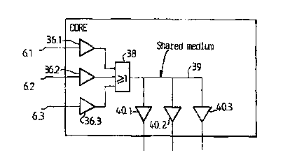
With L~ e}~ce to Fig. 4, illustrating the multiplexing
10 principle in the switch core 1, data on the ~ ; c~tion
rh~nnPl ~ 6 .1-6 . n are received in the switch core in receiver
circuits 36,n, there being in the present example for the
sake of simplicity three circuits 36.1-36.3. One bit rrom a
respective switch port is supplied to the inputs of a
15 generally shown multiplexing device 38 which performs an OR
operation. Only one bit shall take one or the other of the
values 0 or 1 in a time slot, i . e . the bit from the switch
port to which the time slot has been allotted. Further bits
shall be o, whereby these do not actively affect the result
20 of the OR operation, i.e. they have a recessive level.
Contrary thereto, the bit being either 1 or 0 tran-yel~,.,Lly
passes the multiplexing means 38 due to the fact that the
other bits are 0. Thereby multiplexing of data from the
different switch ports is performed. The output from the
25 multiplexing device 38 is connected to a common medium 39
ending in drive circuits 40.n, in the present example for the
sake of simplicity three circuits 40.1-40.3, towards all
switch ports. All switch ports therefore receive data from
all time slots in a respective receiver circuit 20.n, as will
30 be described more closely below.
A po~ihle ~ ; L of the switch core 1 will now be
described with reference to Figs. 5 and 6. As particularly
appears from Fig. 5 the switch core consists of a number of
units 42.n interconnected into a chain, in the present
35 example for the sake of simplicity three units 42.1-42.3, of
which each is associated with a respective switch port 2 . n.
The multiplexing device 38 is distributed on the port
associated units 42.n and is ~ormed by a set of OR gates
38.n(1-8) (cf. Fig. 6) in each port associated unit 42.n,
Wo 9~30319 ~ 1 8 7 6 1 8 ~IDh~ D l73
output6 44.n, e.g. 44.2, from one set of OR gates 38.n(1-8),
e.g. 38.2tl)-38.2(8) in a unit 42.n, e.g. 42.2 being
interconnected with the respective inputs 46. (n+l), e.g.
46.3, of a CuLL~ n~ 6et of OR gatQ6 38. (n+l) (1-8), e.g.
5 38.3(1)-38.3(8) in a later unit 42.(n+1), e.g. 42.3. The
inputs 46.1 of a ~irst set of OR gates 38.1(1)-38.1(8) in a
unit 42.1 is given the value O, as appears from Fig. 5. The
outputs 44.n, e.g. 44.3, of the OR gates 38.n(1-8), e.g.
38.3(1)-38.3(8) in the last port associated unit 42.n, e.g.
10 42.3 in the chain, aVLLe:~Vl~d to the output of the generally
shown multiplexing device 38 in Fig. 4. The mult;rl~Y;n~ is
per~ormed by succes6ive bit by bit OR operations, as will
appear more closely from the description below.
Bus conflict information is guided from one port
15 associated unit to another one in the chain. The output 48.n,
e.g. 48.2 from an OR gate 49.n, e.g. 49.2, of a port
associated unit 42.n, e.g. 42.2, is inteL~ ~.L~-~3 with an
input 50.(n+1), e.g. 50.3 of a VU~L--~ l;ng OR gate
49 . (n+l), e.g. 49.3 in a later port associated unit 42. (n+1),
20 e.g. 42.3 in the chain. The input 50.1 of the OR gate 49.1 in
the first port associated unit 42.1 is given the value 0. The
output 48.n from the OR gate 49.n, e.g. 49.3, in the last
port associated unit 42.n, e.g. 42.3 in the chain indicates,
when it is set to 1 that more than one switch port carries
25 active data in one and the same time slot, which will appear
more closely from the description below.
A port associated unit 42.n is shown more in detail in
Fig . 6 . Data f rom the CVL L -~ .f1; n~ switch port 2 . n on the
~ ;cation channel 6.n is received in 6erial form in a
30 receiver circuit 36.n, cf. Fig. 4, and is pas6ed on to a
~eries/parallel converter 62. From there data is sent in
parallel form to the input 63 of an error dPtec~ ;nrJ and error
isolating device 64.
One form of error, e.g. caused by a short circuit,
35 manifests itself by a switch port staticly driving its output
to a high or low 6tate. A high state is particularly critical
since the mul~;pl~Y;n~ would be completely ~ hl~d if the
error i6 not isolated. Before isolation can be performed the
error mu6t be detected . By the f lag in a storing po6ition 26
.
2187 8
WO 95/303t9 61 r~l c~ 73
11
which is staticly set to 0, high as well as low states shall
appear in each frame. The error can thus be detected by
supervising the ~L ~sc n~e of a static high state.
The detecfinn of a static high 6tate appear6 from Fig. 7,
5 which shows the device 6~ more in detail. All bits from the
converter 62 are supplied to i.a. the inputs of a NAND gate
66. The output of the NAND gate 66 is connected to a 0-
setting input 68 of a counter 70. The outputs 72 Or the
counter 70 are connected to a comparison circuit 74 the
10 output 76 of which is set to 0 if the counter value is equal
to (or exceeds) the number of time slots in a frame. The
output 76 i8 connected to a counter input 78 of the counter
70, and to a control input of AND gates 80, the other input
of which are supplied with data ~rom the input 63. A clock
15 input of the counter 70 is shown at 82.
If any of the data bits on the input 68 of the counter 70
i8 0, the counter i6 set to 0. If, ~.UIILL~L~ thereto, all data
is 1, the counter steps up by one f or each time slot . If all
data staticly consists of only ls during a whole frame, the
20 counter is stopped via the counter input 78 and the outputs
84 of the gates 80 become 0, otherwise the outputs 84 of the
gates 80 reflect data arising from the input 63.
Another form of error, e.g. in the srh~ r, can
mani~est itself by more switch ports ~ n~ the same time
25 slot. Thus several switch ports send active data in one and
the same time slot. The error is detected in the switch core
and is reported e . g . to the srhP~ r in a way not shown.
The outputs 84 from the device 64 are conn~rt~ to an OR
gate 86, which sets its output to 1 when data in a time slot
30 are different from 0. Data ~rom the input 46 are supplied to
the inputs of an OR gate 88. When a data on the input 46
differs from 0 the output from the OR gate 88 will be set to
- 1. The outputs from the OR gate 86 and the OR gate 88 are
connected to the inputs of an AND gate 90, the output of
35 which tG~ with the input 50.n form inputs to an OR gate
49, the output of which in turn forms the output 48.n. The
output rrOm the AND gate 9 0 is thereby set to 1 when data
having appeared in the receiver circuit 3 6 . n of the port
~ssociated unit in question, and data rrom any earlier port
W095/30319 21 8761 8 l~"~ 73 ~
as~ociated unit having appeared on the input 46 both are
active simultaneously. By the OR gate 49 such a state is
fuLw~lded to the next port associated unit. The value 1 on
the output 48.n from the last port associated unit 42.n thus
5 indicates that a bus conflict has been detected in a port
associated unit.
The OR gates 3 8 . n ( 1 ) - 3 8 . n ( 8 ) in a port associated unit
42.n each ac,..._,,u--d to a respective bit of the data in a
time slot. Thus data with 8 bits is ~L~cessed in parallel.
10 Data from an earlier port associated unit in the chain is
~upplied to a respective input of the OR gates 38.n(1)-
38.n(8), one bit to each OR gate. The outputs from the device
64.n are supplied to a respective second input of the OP~
gates 38.n(1)-38.n(8), one bit to each OR gate. Data on the
15 output 50.n is furthermore forwarded to the next port
associated unit in the chain.
The multiplexing is done in a way that OR operations in
the port associated unit in question are performed between
data from an earlier port associated unit, consisting of the
ZO multiplex of data from switch ports b~1 on~i n~ to all earlier
port associated units in the chain, and data from the switch
port 2.n bPlon7;n~ to the port associated unit 42.n in
question. Data resulting on the outputs 44 of the OR gates
38.n and consisting of a multiplex lnrl~ ln~ the data of the
25 switch port 2.n in question, are forwarded to the next port
associated unit in the chain.
The multiplex from the outputs 44.n of the last port
associated unit 42.n is supplied via inputs 94.1-94.n of all
port associated units 42.1-42.n to a respective
30 parallel/series converter 96.1-96.n. Data in serial form is
thereafter sl~rp1~ to the input of a drive circuit 40.n, cf.
Fig . 4, the output of which is connected via a link 8 . n to
the receiver circuit 20.n in the ~;ULL~ in~ switch port.
In the switch port series-to-parallel conversion of data
35 ~rom the switch core is performed in the converter 22.n. By
means of the time switching unit 14 . n the respective switch
port selects the data which is particularly l nt~n~ f or the
fiwitch port and presents this to the line circuit 12 . n. This
can be perf ormed in a way known per se .
~ wo 95130319 2 1 8 7 6 ~ 8 PcrlsEss/ao473
For the sake of simplicity the pro~ PCsi n~ of data h~s
above been assumed to be performed with 8 bits in parallel,
but another width is conceivable as well.
FUL t~ ~ e, operations which have been described as
5 ~n~ltlain~ e.g. OR operations, can be re-formulated in a way
that the operations instead include AND operations, without
this conflicting with the spirit of the invention. For the
man of the art it will be evident how the different
~~';~ ~8 may be changed in this respect.
As an example, the mul~lrlPY1ng device 38 illu;,~L~ted
generally in Fig. 4 and more in detail in Fig. 6 has been
described as performing OR operations. The circuit solutions
shown in the Figures can be easily modified for p6LruL..,ing
the multiplexing by AND operations.
Above it is also indicated as an example, with reference
to Fig. 3, that the flags 26 are given the logical value 1 by
the superior control unit for indicating that the time slot
~-JLL-~ ;n~ to the respective flag has been allotted to a
switch port, and the value O if the time slot has not been
20 allotted to the switch port. However, the opposite could be
the case as well, and also here the required modifications of
the described circuit solutions will be easily realized by
the man of the art. Fur~ h- e the invention, for the sake
of simplicity, has only been described from the point of view
25 of circuit switching. It should however be understood that
the invention can also be applied to a system for integrated
circuit and packet switching . Position ad-lL e~sed data and
packets can share the time on the tr~n-mi q~ n links
int~ o ,~ in~ the switch ports with the switch core, in a
30 way known per se. In that c~nnPc1 ir~n data for circuit
switching may be handled in such a system in accordance with
the invention.