Note: Descriptions are shown in the official language in which they were submitted.
CA 02187653 2004-O1-15
26775-226
1
Sealed Electronic Packaging For Environmental Protection Of
Active Electronics
Technical Field of the Invention
This invention relates to environmental protection
for active electronics. More specifically, this invention
relates to sealed electronics packaging for the
environmental protection of active electronic circuit boards
and the like assemblies. In particular, this invention
relates to environmental packaging which permits access to
the active electronics boards for repair and reconstruction.
Backqround of the Invention
Traditionally, most of the electronics in a
telephony network has been located in the central office or
in a few large electronic installations located remotely
from the central office. These remote electronics are
powered by power drawn from the power mains and backed up by
battery power supplies. The electronics in the central
office operate in an environment with a carefully regulated
temperature and humidity to assure their proper operation.
The remote electronics usually were also installed in vaults
with controlled environments, or at least in enclosures that
were maintained at a temperature above that of the outdoor
environment by the large amount of heat dissipated by the
system.
Recent advances in digital signal processing has
made possible new and more capable transmission systems.
Many of these new systems created a need to move the active
electronic components in the telephone system away from a
temperature controlled central office and out into the
CA 02187653 2004-O1-15
26775-226
la
general environment where the components will be exposed to
wide fluctuations in temperature, humidity and environmental
pollutants. To gain the full
WO 95128072 218 7 6 5 3 PCT~S95104291
-2-
advantage of these new transmission systems it is desirable to deploy the
remote electronics
in very small units that are powered from a central point over the
transmission media. These
power efficient units generate very little heat and so are much more
vulnerable to damage
from moisture than was the case in the past because they lack the internal
heating necessary
to keep them dry. As a result there has been an increasing need to
environmentally protect
these low heat active electronics systems.
The typical small remote electronics unit deployed in the telephone network
will be
installed by technicians with few tools and limited supervision. The service
life of these
electronics is expected to be 20 years. Because these units will be relatively
expensive, it is
also important that they be repairable during production and later when
retrieved from the
field. These systems will also require a full range of component types to
deliver the high
pertormancelcost ratio required by the new network architectures.
Environmentally hardened electronic components exist in the world for military
and
automotive applications. Military equipment relies on the use of carefully
selected and
specially packaged components that are then deployed in expensive sealed
enclosures. The
seals on these enclosures are maintained by the disciplined personnel
following strict
maintenance procedures and the service life of these systems is relatively
short. The
materials used are in the most part metals and ceramics which are impermeable
to moisture
and pollutants. Such hermetic packaging systems are costly for large scale
commeroiai
applications. The automotive industry relies heavily on the use of specially
selected
components that are sealed using polymer potting material. This precludes the
ability to
repair and return the unit to operation. Since these sealed modules contain
relatively small,
inexpensive electronic systems that are unlikely to require repair, the use of
potting materials
has been accepted in this application.
These conventional solutions are insufficient for the new telecommunications
systems
because they rely on a limited set of components; well supervised maintenance
personnel; a
hot environment; and the ability to discard defective units rather than to
repair them.
PCTlU595I04291
\~V0 95/28072 a ;.
-3-
Between the factory and use of the active electronics device such as
assemblies of
microprocessors, dynamic random access memory (DRAMS) andlor other components
such
as resistors, capacitors, transformers, cirouit protection devices, electro-
optical devices and
the like, the devices are often subject to static electricity and other types
of hazards which
must be protected against. This is generally been approached through sealing
the
components in a conductive plastic tube or transparent or semi-transparent
plastic or nickel
coated plastic type bag. However, there has been a complete lack of
recognition that such
components, i.e. electronic devices in the active mode when in operation and
generating heat
can be effectively sealed without overheating in an environmental protection
system that will
permit a subsequent reentry and access to the circuit board or other
electronic devices for
repair of discreet components and reuse of the circuit board or other
electronic device. This
unexpected recognition on behalf of the inventors is a special factor in the
present invention.
Sealing multipin electronic connectors by means of a rubber gasket is well
known.
Connectors sealed in this manner will work where the connection is exposed to
occasional
splashing with water or in situations where drying heat is available or where
the connection is
under a frequent maintenance program. But in situations of long term exposure
without drying
heat, connectors sealed in this manner will become internally wet due to the
transmission of
water vapor through the insulating polymer materials. This moisture will cause
current
leakage and corrosion leading to the failure of the connection. The use of a
baffled barrier
system combined with a selected elastic sealant is uniquely effective in
blocking the these
leakage paths without adversely affecting the mechanical flexing of the
contacts or the surface
physics of the contact. Surprisingly, this combination effectively prevents
current leakage
even if the connector has be mated and demated many times.
The invention pertains to the environmental sealing of active electronics by
means of
an environmentally protecting flexible packaging material including a moisture
barrier therein
combined with a sealed connector system which protects the electronics even
during the heat
generating active operations made without overheating the electronics. The
sealing system
has no impact on the electronics assembly process and may be removed and
replaced many
CA 02187653 2004-O1-15
26775-226
4
times without damaging the electronics allowing full repair
of the electronics. The invention also provides for a
method of making a sealing subassembly into which the active
electronics can be inserted, simplifying the final sealing
of the active electronics. The use of plastic materials in
the seals and packaging produces a non-hermetic package; the
potential harmful effects of moisture and other harmful
chemicals which can diffuse through the plastic materials
can be absorbed by optionally including a small amount of
desiccant/absorbent inside the package. Thus, the invention
provides for the previously desired features as well as many
other benefits obvious to an ordinary skilled artisan upon a
reading of the preferred embodiments.
In accordance with one aspect the invention
provides a protection apparatus for an active electronics
circuit board, the apparatus comprising: a flexible
environmental gas and liquid barrier envelope capable of
accepting the active electronics circuit board, said
envelope being completely sealable around said active
electronics circuit board; and an interconnection device
sealed to the envelope and also permitting the connection of
the active electronics circuit board into an electronics
system outside the envelope.
In accordance with another aspect the invention
provides a protection apparatus for an active electronics
circuit board, comprising a packaging comprising: i) a
flexible environmental gas and liquid barrier completely
sealed around the entire circuit board; and ii) an
interconnection device sealed to the barrier and also
permitting the connection of the circuit board into an
electronics system outside the packaging.
CA 02187653 2004-O1-15
26775-226
4a
Brief Description of the Drawinq(s)
Figure 1 illustrates an environmentally sealed bag
with a sealed pin and socket multipin connector in which the
active electronics can be inserted and subsequently sealed.
Figure 2 illustrates a cross section of an
embodiment of a sealed electronics packaging laminate
construction.
Figure 3 illustrates a cross section of a pin and
socket connector with a conventional sealing gasket.
Figure 4 illustrates a cross section of a pin and
socket connector embodiment which is sealed using an elastic
sealant combined with a baffled construction.
Figure 4b illustrates a mated cross section of a
pin and socket connector in Figure 4 showing the blocked
leakage paths.
Figures 5a and 5b illustrate cross sections of a
sealed pin and socket connector adapter embodiment which is
based on a conventional wire wrap DIN connector.
Figure 6 illustrates a cross section of a sealed
pin and socket connector adapter embodiment which is based
on a custom connector design.
9V0 95!28072 218 7 b J ~ PCT~59u°4291
yr_
Figure 7 illustrates a cross section of a sealed card edge connector adapter
embodiment which employs a sealing barrier design.
Figure 8 illustrates a view of a guide and latch system embodiment to attach
the
electronics board to the adapter without direct access for attachment of the
parts.
Figure 9 illustrates an embodiment mechanically protecting the sealed
electronics
packaging.
Figure 10 illustrates several sealed active electronics modules assembled to
several
sealed back planes interconnected by sealed cable harnesses.
Figure 11 illustrates a sealed active electronics module using a more crush
resistant
bag embodiment.
Figure 12 illustrates an embodiment for extracting large amounts of heat
through the
bag.
Figures 13a and 13b illustrates the parts shown in Figure 12 after assembly
and a
cross section of the heat path.
Figure 13c illustrates an alternative embodiment to remove heat.
Figures 14a and 14b illustrate a sealed active electronics module embodiment
where a
sealed cable is used for interconnection rather than a sealed multipin
connector.
Figure 15 illustrates an environmentally sealed bag embodiment in which the
active
electronics can be inserted with subsequent sealing using a card edge type
connector.
Figures 16, 16a, and 16b illustrate an alternative embodiment for inserting
the
electronics packaging in the environmentally protecting bag using a card edge
type connector.
WO 95/28072 PCTIUS95/04291
2187b53
$_
Figure 17 illustrates another alternative embodiment using a ring type adapter
and a
two piece sheet closure.
Figure 18 illustrates an improved packaging system for use in underground
applications or when the electronics will be possibly submerged under water
for long periods
of time.
The particularly preferred embodiments of the invention will be more clearly
illustrated
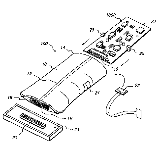
by referring to the appended drawings. More specifically, Figure 1 illustrates
the sealed
electronics packaging 100 of a shape capable of accepting a complete active
electronics
board 1000. Of course, the sealed electronic packaging can have any suitable
shape capable
of accepting the desired shaped electronics board. The packaging can be made
of separate
sheets bonded together or a single sheet folded over as illustrated. More
specifically, the
sealed electronics packaging 100 includes a sheet 10 of an environmentally
protecting
moisture insensitive material formed into a tube that is sized to accept an
active electronics
board 1000.
The tube can be made with either a lap or fin seal. The sheet material 10 is
sealed
either with an adhesive or fused along a longitudinal seam 12 and around an
adapter module
18 with pin contacts 16 passing through the adapter and protruding on the
inside and outside
of the adapter module.
A gas tight seal is constructed around of the pin contacts 16 as they pass
through the
adapter 18 in a manner described below. The pin contacts 16 protruding on the
inside of
packaging 100 are capable of mating with the connector 19 on the electronics
board 23 and
the pin contacts 16 protruding on the outside of the packaging 100 are capable
of mating with
a sealed connector 20 which carries the signals from the active electronics
1000 to the rest of
the system. Stabilizer blocks 25 are attached to the active electronics 1000
to prevent
damage to the electronics. This feature will be described in greater detail
below. The active
WO 95128072 - ~ ~ ~ ~ ~ ~ ~ PCTICTS95/04291
_7_
electronics 1000 are inserted into the open end of the illustrated packaging
100 until the
connector 19 plugs into the connector pins 16 protruding on the inside of
packaging 100. In
some cases the active electronics 1000 will have sharp points extending a
short distance from
it's surfaces. These sharp points could puncture the sheet matertal 10 and
cause a leak. This
sharp point problem can be effectively addressed by first surrounding the
active electronics
1000 with an extruded plastic mesh tube with large holes, plastic foam, fish
paper, or paper
containing desiccant materials. These matertals are inexpensive, will not
affect the heat
transfer, and are thick and tough enough to prevent the sharp points from
touching the sheet
10. After the connector 19 is engaged a packet of desiccant/scavenger 22 is
inserted into the
open end of the packaging 100 and the back edge 14 is sealed using a simple
heat sealing
machine.
Alternatively, this seal could be made using a get type sealant and a metal
clip, velcro,
or extruded zipper. These types of seals have the advantage that they can
easily be opened
and reclosed. Once this seal is complete the active electronics 1000 is
protected from the
effects of moisture and other pollutants. In some cases it is necessary for
the user of the final
assembly to view lights that are attached to the edge of the active
electronics 1000. A
transparent window 21 is provided in the sheet of material 10 through which
these lights may
be seen. Preferably the window is moisture impervious such as plastic plus ITO
coating.
Optionally a one way valve can be included into the bag to out-gas excess
pressure if the bag
were sealed at sea level and then moved to a high altitude application or
preferably slack
volume can be introduced durtng final sealing so that with temperature or
pressure changes
during operations, the volume of the flexible laminate barrier can change
without generating
internal pressure. A suitable temperature operating rang is from about -
40°F to about 200°F.
The pressure will vary from a water head of about 20 feet to an effective
altitude of about
20,000 feet.
The layers of material 10 and parttcularty the preferred embodiments are
descrtbed in
Figure 2, and generally must resist the ingress of moisture resist puncture by
any sharp
protrusion and maintain its integrity for the life of the product. Any
laminate or substrate
material capable of resisting puncture, withstanding chemical environments,
and temperature
extremes while maintaining a high level of protection against moisture ingress
and other
CA 02187653 2004-O1-15
26775-226
8
environmental hazards and the like is suitable for use in
this invention. Particularly, materials which are known to
be stable and consistent over time in these environments are
suitable.
A preferred laminate construction would be of
sufficient thickness to be handled without puncture, tear or
loss of seal integrity. Ranges for the layer thickness are
up to 12 mils for the outside layers, 4 mils for the inside
layers, and 1 mil for the middle layer. A particular sheet
material 10 comprises top and bottom layers of a suitable
material such as high density polyethylene about 6 mils
thick and interior layers of ionomer about 2 mils thick and
a center layer 1 mil of a metal such as aluminum or other
suitable material. Interlaminar bond strength should remain
above 2 lbs./inch as per ASTM D 1876-93. Optionally the
interior surface of the material may be made black to absorb
heat radiated by the active electronics during operation.
Additionally the exterior and or the interior surfaces may
be made with an antistatic coating to reduce electro-static-
discharge ESD potential. In certain environments the
envelope is an inner and an outer layer of plastic with a
central metal layer. Suitable thicknesses are 15 mls.,
1 mls. and 15 mls., respectively.
The general performance of the sheet material must
pass the following specifications: the puncture resistance
of the material when tested using ASTM F 1306-90 with a
screwdriver type tip should be greater than 25 lbs., and
with a pin type tip should be greater than 15 lbs.
Preferably the screwdriver puncture resistance should be
greater than 30 lbs and pin resistance 20 lbs. The
CA 02187653 2004-O1-15
26775-226
8a
material should have a tear resistance of greater than
8 lbs, preferably greater than 12 lbs. when tested according
to ASTM D 2582-93. The heat seal obtained at the seams of
the laminate when formed into a pouch should resist
separation by a force of greater than 30 lbs. most
preferably greater than 35 lbs. when tested to ASTM D 1876-
93. These performance characteristics should not degrade
significantly with time or environmental exposure.
A suitable laminate is illustrated in published
PCT application WO 92/19034, but any laminate layer capable
of resisting puncturing while providing inhibition to
moisture ingress and protection from environmental hazards
such as pollution and the like is suitable for use in the
invention. Figure 2 illustrates a preferred laminate
construction.
W095128072 218 l 6 5 3 PCT~S95/0429t
_g_
Ranges fior the layers can be between about 75 and 350 microns for layers 10a
and
10e between about 20 to 200 microns for layers 10b and 10d, and between about
5 to 75
microns for layer 10c. The particular sheet material 10 comprises top and
bottom layers 10a
and 10e of a suitable material such as low density polyethylene about 200
microns (8 mls
thick) and two interior layers about 80 microns (3 mls thick) of cast
polyamide or polyester and
a central layer of about 20 microns (1 ml thick) of aluminum or other suitable
material.
Optionally but not illustrated, the interior of surtace of the material may
include a black paint or
other material to absorb heat radiated by the active electronics during
operation. By interior it
is meant that portion of the sheet which upon welding into an envelope or an
enclosure will
have the black sides facing each other on opposite sides of the electronics
board.
In some cases it is desirable that the laminate have a three dimensional shape
rather
than be flat. This can be achieved by forming the sheet before welding. If a
large volume
enclosure is required, the aluminum layer could be replaced with a highly
plastic metal such
as commonly found in tin, tin alloys, and the like to sustain large
deformations. The material
used to make window 21 must also, as much as possible, block the transmission
of moisture,
chemical pollutants, and electronic noise while remaining transparent. This
can be
accomplished by using transparent plastics coated with thin coatings of
inorganic materials
such as indium tin oxide (ITO), Si02, doped Ti02, doped AL203, and the like..
For example a
multilayer laminate made of polyester and low density polyethylene can be used
with or
without the inorganic coating.
The sheet material 10 can be fused to the adapter 18 ifi the inner layer of
the flexible
laminate and the adapter are made out of similar polymer materials. Fusion is
the preferred
approach. For example, making the adapter out or polyethylene or a suitable
thermoplastic
material common to both packaging and injection molding, and making the inner
layer of the
sheet material also of the same material, by applying sufficient heat to the
area the materials
will fuse together. Additionally, having the outer layer of the material match
the adapter
material would allow the outer layer to flow and bond with the adapter
material, covering the
raw edge of the sheet material.
CA 02187653 2004-O1-15
26775-226
Alternatively the edges can be adhesively sealed
to form the closure. In a preferred embodiment, the sheet
material 10 is sealed to the adapter 18 by means of a hot
melt adhesive or a reactive hot melt adhesive. Specifically
5 a styrene-butadiene-styrene, SBS polyamide or polyester
based hot melt adhesive or thermosetting epoxy, polyurethane
or polyester could be used. It is important that high
frequency noise be blocked from passing through the
packaging 100 by enclosing the active electronics 1000 in a
10 conductive layer. The foil layer in the sheet material 10
may be effective for this purpose, and a conductive layer
can be deposited on the inner surfaces of the adapter 18 by
a variety of processes such as vapor deposition, plating, or
painting with conductive paint. Care must be taken to avoid
shorting out the connector pins 16. To connect the foil
layer in the sheet material 10 to the conductive layer on
the inner surface of the adapter 18, an electrically
conductive hot melt adhesive may be used.
Electrically conductive hot melts can be
formulated by the addition of conductive fillers to standard
hot melt adhesives. Descriptions of such materials and also
alternatively ferromagnetic fillers could be used so that an
alternating magnetic field will provide the heating during
assembly. Raychem's US Patent No. 5,378,879 describes such
materials.
Even with these measures, a small amount of
moisture (about 30 micrograms/hour) and pollutants such as
H2S, 502, C12, and N02 will be transmitted through the polymer
seals of packaging 100 and damage the active electronics
1000. A desiccant/scavenger packet 22 addresses this
CA 02187653 2004-O1-15
26775-226
10a
transmission issue where it poses a problem. The package
absorbs this small quantity of moisture and pollutants over
the 20-year life of the system. In the preferred
embodiment, silica gel, alumina, and molecular sieves are
used to absorb moisture and polluting gases. Naturally, it
is important that the desiccant/scavenger packet 22 be
maintained in a dry, unreacted state until it is time to
seal the packaging 100. It is also important that the
packet 22 never be accidentally left out of the packaging
100 during final assembly. The packet 22 is anchored inside
the packaging 100 such that the clear view through the
window 21 is retained.
WO 95128072 ~ PCT/US95/04291
-11-
In the preferred embodiment, the desiccant/scavenger material is sealed in a
polyethylene bag with a moisture vapor transmission rate sufficiently high to
keep the relative
humidity low inside the sealed electronic package but tow enough to protect
the desiccant
from the humidity before the electronic package is sealed. Alternatively, the
desiccant/scavenger material is sealed in an impermeable package that has a
hole punched
on one side. This hole is sealed by an adhesive patch attached to a long
colored ribbon.
Using a pressure sensitive adhesive, the pack is attached in a convenient
location inside the
packaging 100 with the ribbon passing out of the open end and with its free
end attached to
the outside of the packaging 100. Before the final sealing of the back edge 14
can be done
the assembler must pull out the ribbon thus exposing the desiccant/scavenger
at the last
moment before the final seal is made. After this final seal is made, the seal
integrity can be
tested by heating the sealed electronics packaging 100 in an oven for a few
minutes or hours.
The heat will cause the air in the packaging 100 to expand and leak out or
visibly expand the
package envelope of a properly sealed unit. When the units are returned to
room
temperature the leaking ones will collapse and be readily detected.
Alternatively, before the
final seal is made, a pressure test can be pertormed by inserting a rubber
stopper into the
open end of the package with air pressure connected through the stopper and
lowering the
system into water. By pressurizing the package under water any leakage will be
visible as air
bubbles. A further alternative test is a vacuum or a squeeze test which can be
used for the
same purpose.
The effective seating of the active electronics 1000 also requires sealing the
pin
connectors 16 when engaged with the connector 20 to provide an overall sealed
system.
Figure 3 illustrates the cross-sectional view of a commonly available sealed
connector. It
consists of a male pin half 1900; a sealing gasket 1901; connector pins 1902;
a female half
1903; and connector receptacles 1904. When the male half 1900 is mated with
the female
half 1903 the sealing gasket 1901 is pressed tightty against the connector
housing top 1910
making a seal. In accordance with the present invention, if the connector
backsides 1911 and
1912 are sealed by potting material or by the packaging 100, then water cannot
leak into the
cavity around the connector receptacles 1904. This type of connector design
will prevent the
formation of conductive paths within the connector for a short period of time,
but because
moisture and pollutants can transmit through the molded plastic polymer
holding the pins, if
CA 02187653 2004-O1-15
26775-226
12
continuously exposed to high humidity and pollution, the
cavity surrounding the receptacles 1904 will eventually
become wet and contaminated. This contamination will
provide leakage paths between the pin connector receptacles
1904 and corrosion of the pin receptacles 1904 and the pins
1902 will take place, degrading the quality of the
connection.
Figure 4 and 4b show a partial cross-sectional
view of the connector of the preferred embodiment that
provides a greatly improved sealed connector. The male half
2000 is identical to the conventional male half 1900 but the
construction of the female half 2003 differs from the female
half 1903. The female half 2003 is fabricated by inserting
the receptacles 2004 into a polymer base plate 2016. Then a
polymer upper cover 2015 is installed over the receptacles
2004. The upper cover 2015 is molded with baffles 2013 that
surround each receptacle 2004 and extend almost to the base
plate 2016. A hydrophobic sealant material such as a grease
or preferably an elastic gel is added into the female half
2003 to almost completely fill the cavity in the female half
2003. Silicone gels as described in U.S. Patents 5,111,497;
5,246,383; and 5,376,019 are particularly suitable for this
purpose because the gels will adhere to the surfaces inside
the connector and yet are sufficiently elastic that the gels
will not interfere with the deflection of the receptacle
during insertion of the pin contact 2012. These gels are
extremely effective at keeping water off of metal and
plastic contact surfaces. Preferred gels include the
property of being hydrophobic.
CA 02187653 2004-O1-15
26775-226
13
Female connectors with baffles for the support of
the contacts are commonly available. The DIN connector
series (Per DIN 41612, IEC 603-2) manufactured by T&B and
other manufacturers contain baffles which prevent the
accidental contact of the receptacles 2004 and to support
small wedges that hold the elastic arms of the receptacles
2004 in a pre-stressed state beneficial to making a good
contact. These structures are serendipitously useful for
the purpose of sealing. An additional surprising benefit of
a silicone gel material is that its extremely low surface
energy causes it to wet to surfaces aggressively. The large
surface area produced by the internal baffles 2013 makes it
possible to fill the connector cavity by simply pouring the
uncured gel through the small holes in the housing top 2010.
The low surface energy allows the liquid to creep through
the holes, coat the walls of each interior surface and fill
the connector completely.
A viscosity of less than 1000 centipoise,
preferably about 800 centipoise, for the uncured gel is
sufficiently low to permit filling a connector with a
distance between pins of about .10 inches. The presence of
gel or grease in the female half 2003, particularly at the
bottom where the polymer base plate 2016 meets polymer upper
cover 2015 and the baffle 2013 will prevent the formation of
a moisture and contaminant track between the receptacles
2004. This gel or grease should be sufficiently soft to
allow encapsulation of the mating pins in the male half 2000
without excessive force. A hardness in the range of 15-50
grams as measured by a texture analyzer using standard MQC
procedures will satisfy these conditions. U.S. Patent
4,852,636, completely incorporated herein by reference for
CA 02187653 2004-O1-15
26775-226
13a
all purposes, teaches a procedure known to the ordinary
artisan for determining gram hardness of a material. This
is sometimes referred to as Voland hardness. The gasket
2001 in the male half 2000 could be made of rubber or gel
material with a higher elastic modules and hardness. A
hardness in the range of 30-70 grams will satisfy the
requirement that the gel or rubber in the male half must
withstand multiple re-entries without damage to the gel
sufficient to cause it to lose its sealing capability. A
gel with a hardness of 30-50 grams will satisfy the
requirements of both the female half 2003 and the male half
2000 and could be used interchangeably in both areas. The
gel material has the advantage that it will readily break up
moisture tracks on the housing top 2010 because of the
hydrophobic properties of the gel material. Thus the
connector could be mated with moisture present on the
surfaces and a high insulation resistance could be achieved.
The gel type gasket is preferably cured in place
to achieve a high adhesion with the male half 2000. In an
alternative embodiment, this gel type gasket could be
fabricated by punching out an open cell foam reinforced gel
sheet as described in detail in US Patent 4,865,905 and US
Patent 5,588,856. These gaskets can be retained in place by
molding gripping features into the adapter 18 (Fig. 1) or by
means of a mechanical frame that snaps or screws into place.
Figure 4b illustrates another advantage of this
design. V~lith frequent mating and demating cycles the
mechanical stress in the gel is high only on the material
near the top of
WO 95128072 218 7 b 5 3 P~~S95104291
-14-
the cavity in the female half 2003 so loss of gel and the production of voids
2100 that can
become moist tends to be only in this area. These voids, however, are isolated
from each
other by the gel sealing the lower path 2101 between the receptacles at the
bottom of the
female half 2003 and by the gel or rubber gasket 2001 pressed on the housing
top 2010 that
blocks the upper path 2102. In some cases a coaxial connector will be used to
interoonnect
high frequency signals into the active electronics 1000. The same sealing
technique can be
used with this type of connector where the center female contact is filled
with gel to prevent
shorting leaks from the center contact to the ground.
Figures 5a and 5b illustrates a cross-sectional view of the adapter 18 or 18b
installed
in an injection molded part 2201 or 2201b (18 in Fig. 1) and sealed using a
potting material
2203 or 2203b such as a 2 part curable polyurethane or epoxy compound. Figure
5a is the
male-female embodiment while Figure 5b is the female-male embodiment. The main
d'rfference is socket 2250 in Figure 5a and the pin embodiment 2240 in Figure
5b. Identical
parts are labeled the same while alternative embodiments include "b" next to
the number in
Figure 5b. Subsequently, the flexible sealing bag 10 is bonded to the molded
part. To
prevent the leakage of the potting material during the potting process, a
close fitting plug can
be inserted in place of the gasket 2001 until the potting material cures.
Figure 6 illustrates a alternative adapter design where the contact pins 16
are inserted
or molded directly into the molded adapter part 2211. As in Figure 5, the
sealing bag 10 is
subsequently attached. This embodiment saves the potting step and in essence
creates a
one part DIN connector interface between the interior of the bag and the
outside environment.
In Figures 5a and 5b but also useful with Figure 6 embodiments, the backplane
board 2260
includes sockets 2261 potted 2262 in the board. The sealed electronics plug
into the
backplane board 2260.
Figure 7 illustrates the method of sealing a card edge type connector 2300. A
sealing
gasket 2301 is attached to the adapter 500 so that when the connector is
plugged into the
female half 2320 the gasket 2301 will be pressed tightly against the lip of
the female half 2320
and the sealing ring 2330. To further block the leak paths in the female
connector 2320 gel
can be deposited into it.
W O 95128072 218 7 6 5 3 P~~S9~0429I
-15-
Figure 8 illustrates a guide and latch mechanism that permits the active
electronics
1000 to be plugged into the connector pins 16 protruding on the inside of the
adapter 18.
Guiding ribs 2210 are used to safely guide the active electronics 1000 into
engagement with
the connector pins i6 protruding on the inside of the adapter 18. A latching
hook mechanism
2211 will then fall into a hole 2212 in the active electronics board holding
it securely to the
adapter 18. Preferably, the latching hook 2211 includes a tactile and positive
lock to prevent
unwarranted unlocking of the board under vibrating conditions as well as
providing a positive
sense of when the board is locked in place to the connector. A compliant latch
structure, e.g.
spring loaded, and a compliant cushion, e.g. foam rubber, installed at the
bottom, i.e. base, of
the guiding ribs 2210 along and adjacent the rectangular face of the adapter
18 can be used
to reduce forces on the active electronics 1000 when they are accidently
dropped during
handling.
If the sheet material 10 is relatively thin and flexible it would be possible
to damage the
active electronics 1000 (not visible) by pressure on the outside of the
packaging 100. Figure
9 illustrates a method of preventing this problem in situations where the
module may receive
rough handling. After sealing the package 100 the assembly is inserted into a
protective box
101. The adapter 18 could be designed to fd closely to the open end of the
protective box 101
with provisions for screws or other fasteners to hold the parts together
forming a finished
electronic module 102. If screws are used, then the module 102 can easily be
opened later to
make repairs on the active electronics 1000. To permit the active electronics
1000 to be
gripped and stabilized by the protective box 101 spacer blocks 25 (Fig. 1 )
are attached to the
active electronics 1000 before seating the sheet 10. These blocks, optionally
foam blocks, are
sized to just fit inside the protective box 101. This will prevent damaging
flex of the active
electronics and the connector 19 during handling and vibration and also help
protect the
flexible laminate. In the preferred embodiment, the protective box 101 is blow
molded and
holes are provided to drain water and to permit the viewing of the fights on
the active
electronics 1000.
Figure 10 illustrates the assembly of several modules 102 to a sealed back
plane 203.
Each back plane has several female connectors 204 electrically connected to a
back plane
WO 95/28072 PCTIUS95104291
2187653 1
-,6-
circuit board and then potted to exclude moisture from the back side. Wires
also connected to
the backplane circuit board carry the signals to sealed terminal blocks 205.
Once the
modules 102 are plugged into the sealed female connectors 204 a totally sealed
system is
provided to protect the electronics. An additional advantage of individually
sealing each active
electronic circuit is greater reliability. If one leaks, the others are still
unaffected. Also,
humidity sensors can be included in each sealed electronics package 100. If
any one of the
units becomes moist an alarm is sounded and that unit can be replaced.
The protective box 101 has the disadvantage of reducing the heat transfer of
the
system and adding extra cost and bulk. In some cases, where only a moderate
amount of
mechanical protection is required, a more rigid sheet material 10 can be used,
where the
metal foil thickness is increased for greater bend resistance. Figure 11
illustrates a closure of
this type were the heavy sheet material 200 is heat sealed into a tubular
shape that will just fit
over the adapter 218. A hot melt bond between the adapter 218 and the sheet
material 200
can be made or preferably a heat shrinkable band 202 with a hot melt adhesive
on the inside
is shrunk over the joint between the adapter 218 and the sheet 200. The back
end can be
closed by heat sealing and folding in the manner of a milk carton or by
inserting a plug with a
shape similar to the adapter 218 and sealing in a like manner.
In some cases the heat produced by the active electronics 1000 will be quite
high.
The main impediment to the transfer of this heat out of the package is the
insulating layer of
air inside the sheet 10. The thermal resistance of the sheet 10 itself is
quite low, since it is
very thin and made largely of metal. Figure 12 illustrates a means of
thermally coupling a hot
component on the active electronics 1000 board through the sheet 10 and into a
heat
spreader 250 in the free stream air. Figure 13 illustrates the assembly of the
parts in Figure
12. After sealing the sheet 10 the heat spreader 250 is clamped on to the
active electronics
1000 at the point where the stabilizer blocks 25 are attached. From section A-
A in Figure 13a
and 13b it can be seen that the hot component 252 which is attached to the
active electronics
1000 is pressed in contact with a thermally conductive gel pad 251 that has be
preinstalled on
the hot component 252 or inside the sheet material 10. A suitable thermally
conductive gel
251 formulation for this purpose is described more thoroughly in US Patent
4,852,646,
incorporated herein by reference. An additional pad of thermally conductive
gel could also be
W095J28072 218 7 6 ~ ~ P~T~S95/04291
-17-
applied between the outer surface of the sheet 10 and the heat spreader 250 to
further
improve the transfer of heat through the sheet 10 to the heat spreader. Figure
13c shows an
alternative approach to remove heat from hot component 252. A bolt, 253,
penetrates the
flexible laminate and connects directly to 252. A sealing material seals
between the flexible
laminate and the hot component.
In some cases only a few fairly permanent connections from the active
electronics
1000 are required. Figure 14 illustrates a low cost method of providing
packaging for this type
of system. A connector 301 is attached to a wire harness 303 which is then
insert molded into
and adapter 302. To achieve a reliable seal it may be necessary to remove the
insulation
from the wire in the harness 303 in the area where it passes through the
adapter 302 to block
the flow of moisture under the insulation of the wires in harness 303.
Alternatively a curing
blocking material could be used or a blocked wire that is fabricated with a
blocking agent
between the wire and the insulation. To assemble the active electronics into
the packaging
100 the active electronics 1000 is inserted into the open end of the packaging
100 until the
latch features 304 molded onto the adapter 302 engage the holes 305 in the
active electronics
1000. Once firmly attached in this manner, the connector 301 can be connected
to the mating
connector 300 on the active electronics 1000. After the desiccant/scavenger
packet has been
activated the open end of the sealed electronics packaging can be sealed as
usual with a heat
sealer. Figure 14b illustrates another embodiment and potentially a lower cost
method of
sealing the electronics. A flat cable 306 is connected to connector 307. The
flexible laminate
barrier is installed over the circuit board 1000 and heatsealed with hot melt
adhesive to the flat
cable 306 and fused to itself on both sides of 306 to form a complete moisture
vapor barrier
around 1000.
In some cases it will be preferable to use a card edge type connector rather
than a pin
and socket type to interconnect the active electronics 1000 through the sealed
electronics
packaging 1000. Figure 15 illustrates a simple method of accommodating this
type of
connector. A band of hot melt adhesive 420 is install around the card edge
connector which
as been fabricated to provide space for this application. Care must be take to
assure that the
contact fingers of the card edge connector 428 are not contaminated with this
adhesive.
Alternatively the adhesive could be insert molded on the card edge extension.
The sheet
WO 95128072 PCTIUS95/04291
2187653 i
material 10 is welded into a closure 410 with one open side 414. The active
electronics 1000
are inserted into the closure 410 and the open edge 414 is heat sealed closed
over the hot
melt adhesive 420. A modified bag sealer with appropriate relief for the area
near the card
edge connector is required for this operation. Altemat'rvely, a card edge
adapter could be
fabricated using a small paddle card and a female card edge connector. The
adapter would
be preassembled into the closure 410 with the side of the closure opposite the
adapter left
open. For final assembly the active electronics 1000 would be inserted into
this open side
and plugged into the female connector inside the closure. Then the open side
could be heat
sealed using conventional heat sealer. This alternative approach has the
advantage of
simplifying the heat sealing operation performed by final assembler.
Figures 16, 16a, and 16b illustrates another configuration of sealed
electronics
packaging for use with card edge connectors. An adapter 500 is sealed to the
active
electronics using and appropriate potting material 505. The closure 510 will
seal to the
adapter 500 which includes the active electronics board, at a U shaped member
illustrated in
figure 16a and i6b with a pressure ring 520 which will be ultimately encased
between the
hard outer box 530 and base member 500 more spec~cally, 16b illustrates in
partial cross
section the process of inserting the active electronics board 1000 and sealing
to the base
member 500.
A further alternative is illustrated in Figure 17. In this embodiment the
adapter 618 is
extended to from a complete ring around the active electronics 1000. The
active electronics
are plugged into the interior pins of the adapter connector 616 and then two
sheets 10 are
heat sealed or welded to the adapter ring 625. For additional strength a
forming tool 620 can
be used to form a secure lip 630 to hold the sheets 10 in place.
Fgure 18 shows an improved packaging system for use in underground
applications
when the electronics will be possibly submerged under water for long periods
of time. A bell
jar 700 is placed over the sealed electronic modules 702 and the backplane
701. The belljar
keeps liquid water from 701 and 702.
WO 95J28D72 PCT/US95/04291
~~~~6~3
_19_
The invention resides at feast in part in the unexpected realization by the
inventors that
in spite of past thinking, the active electronics could be sealed in an
appropriate laminate,
protected from the environment, and still operate in harsh environments while
permitting re-
entry to the package by splitting of the package 100 upon return to the
factory.
The invention has been described with respect to the previous particularly
preferred
embodiment. Modifications obvious to the ordinary skilled artisan are intended
to be within
the scope of the invention. For example, the aluminum metallic sheet might be
copper silver
gold or other suitable material. The plastic laminate could be a one sheet
fused to the metallic
layer and folded over and fused to itself. The bag itself might have a sealed
entry port in the
event that the bag was not to be discarded upon requiring access to the active
electronics to
make repairs, and the like.