Note: Descriptions are shown in the official language in which they were submitted.
CA 02188444 1996-10-21
~' ~ ~~L~44
- - BUILT IN TEST FOR DYNAMIC RASTER VIDEO OUTPUT
GOVERNMENT RIGHTS
The United States Government has rights in this invention pursuant to Contract
No. F33600-88-G-S 107, awarded by the Department of the Air Force.
BACKGROUND OF THE INVENTTON
The invention relates generally to testing the output of video display
generators
and, in particular, to a dynamic video test for the single or multiple channel
video output
of a color or monochromatic-type video display generator.
Video display generators are used to output on one or more channels analog
video signals created from digital raster data. These analog video signals
create color or
monochromatic ("mono") video images. A mono image is generally created from a
mono signal on a single video channel, while a color image is generally
created from
several distinct color signals, each on a separate video channel. For example,
a standard
red, green and blue (RGB) color image is created from a red, a green and a
blue analog
video signal, each being output from a video display generator on a distinct
output
channel. The video display generator may also output an overlay image (which
"overlays" the video image) on a separate video channel. Within each channel,
a mono
or color output video signal may have several distinct components, including
an "active
video" portion, a "video blank" portion and a "video sync" portion, all of
which are well
known in the art and are not described in detail herein.
To create an analog video signal from digital raster data, a video display
generator must retrieve the digital data from memory to create a digital
signal. The
display generator then creates an analog signal from the digital signal with a
digital-to-
analog (D/A) converter. The analog signal is then amplified and displayed as a
video
image.
During the video image creation process, many factors adversely affect the
analog video signal output from the display generator. For example, signal
interpolation
within the D/A converter introduces distortions to the analog signal. These
distortions
are then magnified during amplification of the signal. In addition, the analog
amplifier,
which functions differently at different signal frequencies, creates further
distortion in
the analog output. Because of the non-linearities introduced by the elements
of the
video display generator, the output analog signal is not a completely accurate
AMENGcD S~-iEET
IPFAtEP
CA 02188444 1996-10-21
-2-
representation of the digital data from which it was created. Although
perfectly accurate
video images cannot be expected, it is often necessary to ensure that the
displayed image
is as accurate a representation of the digital data as possible.
Prior art references include U.S. patent 4,772,948 which describes video
analog
S self test hardware for a color graphics display system. The hardware is for
testing the
system elements between the frame buffer and the CRT display monitor.
SUMMARY OF THE INVENTION
The invention provides a dynamic video test for analog video signals created
by a
video display generator from digital raster data. The invention retrieves
analog video
signals from one or more output video channels and digitally compares the
signals to the
data from which they were created. The test results are stored until
retrieved.
In addition, the invention provides a test for dynamic video output of a video
display generator which separately tests each of the video components of an
analog
video signal. The test results for each of the components are stored until
retrieved.
According to one aspect of the invention, the invention comprises a test
apparatus for dynamic testing of a plurality of analog video signals created
from digital
raster data, each of the analog video signals having a plurality of analog
signal
components, the apparatus comprising an addressing means for selecting one of
the
analog signals, a selection means for selecting a desired analog signal
component from
the selected analog signal, an A/D converter which converts the selected
analog signal
component into a digital signal component, an extracting means for extracting
a
characteristic value from the digital signal component, a memory which stores
predetermined characteristic value range data, a comparator for comparing the
characteristic value to the stored characteristic value range data to produce
a result, a
combination means for creating a combination of the result and an address of
the analog
signal component selected by the selection means, and storage means for
storing the
combination created by the combination means.
In another aspect of the invention, the invention comprises a test apparatus
for
dynamic testing of an analog video signal, comprising an ADD converter which
converts
the analog video signal into a converted video signal, an extracting means for
extracting
a characteristic value from the converted video signal, a memory which stores
predetermined characteristic value range data, a comparator which compares the
AMEI~IG~G ~~ctT
lp~~i/EP
CA 02188444 1996-10-2 i ~ ~ z~ ~~
-3-
characteristic value to the stored characteristic value range data to produce
a result, and
storage means for storing the result.
In yet another aspect of the invention, the invention relates to a test
apparatus for
dynamic testing of a plurality of analog video signals, comprising an
addressing means
for selecting one of the analog video signals, an A/D converter which converts
the
analog signal selected by the addressing means into a converted video signal,
an
extracting means for extracting a characteristic value from the converted
video signal, a
memory which stores predetermined characteristic value range data, a
comparator which
compares the characteristic value to the stored characteristic value range
data to
produce a result, and storage means for storing the result.
According to another aspect, the invention relates to a method for dynamic
testing of an analog video signal, comprising the steps of converting the
analog video
signal into a converted video signal, extracting a characteristic value from
the converted
video signal, storing predetermined characteristic value range data, comparing
the
1 S characteristic value to the stored characteristic value range data to
produce a result, and
storing the result.
In another aspect of the invention, the invention relates to a method for
dynamic
testing of a plurality of analog video signals, comprising the steps of
selecting one of
the analog video signals, converting the selected analog video signal into a
converted
video signal, extracting a characteristic value from the converted video
signal, storing
predetermined characteristic value range data, comparing the characteristic
value to the
stored characteristic value range data to produce a result, and storing the
result.
BRIEF DESCRIPTION OF THE DRAWINGS
Figure 1 is a functional block diagram of a preferred embodiment of the
invention;
Figure 2 is a schematic diagram of a preferred embodiment of the invention;
and
Figures 3A and 3B are a flow diagram showing state transition in a test cycle
of
the embodiment of Figure 2.
DESCRIPTION OF THE PREFERRED E1VIBODIMENTS
Preferred embodiments of the invention will be described in detail with
reference
to the accompanying figures.
E
/'~.n~~~.'L.~'4l..GiJ C)i'~ '~C~
(c=w. i.i~~_.
CA 02188444 1996-10-21
-4-
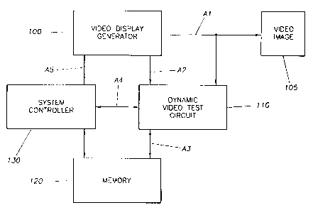
Figure 1 shows a video system including a dynamic video test (DVT) circuit
110. A video display generator 100 outputs analog video signals A1 which are
used to
create a video image 105. The DVT circuit 110 receives the analog video
signals A1, as
well as the digital video signals A2 from which they were created. The digital
signals A2
are then used by the DVT circuit 110 to retrieve predetermined values A3 from
a
memory 120. The DVT circuit 110 compares the analog video signals A1 to the
values
A3 from memory, thereby producing status results A4. The status results A4 are
then
retrieved from the DVT circuit 110 during a read video status operation of a
system
controller 130. The system controller 130 uses the status results A4 to create
control
signals AS which adjust the output of the video display generator 100.
Figure 2 is a schematic diagam of a preferred embodiment of the built-in
dynamic video test (DVT) of the invention. In this embodiment, red, Been and
blue
analog video signals AS1, AS2 and AS3 are output on video channels V1, V2 and
V3 by
a video display generator 100. Within the video display generator 100, digital
raster
data is retrieved from a video memory 102. Any overlay data is enhanced, if
necessary,
by a "double draw" field programmable gate array (FPGA) 104, which will be
described
in more detail below. Red, Been and blue color values are then determined from
a look-
up table (LUT) 106, which outputs red, blue and green digital video signals
DS1, DS2
and DS3. Analog signals are created from these digital signals by digital-to-
analog
(D/A) converters 108A, 1088 and 108C, amplified by analog amplifiers 110A, 11
OB and
11 OC, and output as analog video signals AS 1, AS2 and AS3 by output current
buffers 112A, 1128 and 112C.
The double draw FPGA 104 is a device which enhances overlay data prior to the
creation of the corresponding signal. An overlay image is an image which is
laid over
another image. For example, the video display generator in an airplane may
overlay a
flight path image onto an image of the terrain below. Because an overlay image
may at
times be only a single pixel in width, the overlay image may be very difficult
to
distinguish from the primary image. The double draw FPGA 104 solves this
problem by
examining digital overlay data for areas which are only a single pixel in
width. When
such an area is found, the double draw device widens the overlay image by
placing the
single pixel overlay data into several pixels immediately adjacent the overlay
data pixel.
In this manner, the double draw FPGA 104 enhances the clarity of an overlay
image.
AAJ~~=n'r~"~ c,
_ ...u .>>r?E~""
~ i3 ;~ ;~ ~ ~ _,."
CA 02188444 1996-10-21
v ~ ~~~~4~
-5-
The built-in test is conducted, one channel at a time, by verifying that
"active
video", "video blank" and "video sync" components of the analog video signals
conform
to criteria predetermined from the corresponding digital video signals. The
analog video
channel to be tested is selected by a video multiplexer (mux) address
generator 12. The
video mux address generator 12 is a small counter incremented by a VIDEO MLTX
ADDRESS CLOCK signal S 1, which is generated by a state machine 10 which
controls
the test process. A video mux 14 uses a VIDEO MLJX ADDRESS signal S2 created
by
the address generator 12 to select the appropriate output channel V 1, V2 or
V3, and to
retrieve the corresponding analog video signal AS 1, AS2 or AS3. The chosen
analog
video signal is passed through amplifier 16 to analog-to-digital (AJD)
converter 18,
where it is converted into a p-bit digital signal S7 when the A/D converter 18
receives a
CONVERT CLOCK signal S3 from the state machine 10. At the same time that the
analog video signal is retrieved by the video mux 14, the VIDEO MLJX ADDRESS
signal S2 notifies an LUT data bus mux 20 to retrieve a corresponding n-bit
digital video
signal DS1, DS2 or DS3 from the LUT 106 within the video display generator
100. The
video channel address carried by the VIDEO MUX ADDRESS signal S2 remains
unchanged until the test cycle for the corresponding video channel is
completed, at
which time the address is incremented to prepare the DVT circuit 110 to test
the next
video channel. The bit sizes of the above p-bit and n-bit signals may be
determined by
the user of the dynamic video test circuit.
A test on a selected video channel does not begin until a stable video. signal
is
detected by a double pixel detection circuit 22. This circuit monitors the n-
bit digital
video signal selected by the LUT data bus mux 20 for data values which are
equal for
two successive cycles of a PIXEL CLOCK signal S4 generated by the system
controller
130. When latches 22A and 22B in the double pixel detection circuit 22 output
the same
n-bit digital signal, a digital comparator 24 sends a DOUBLE PIXEL signal SS
to the
state machine 10, forcing the state machine 10 out of its initial state (state
0). However,
the double pixel detection circuit 22 is not limited to the detection of only
two
successive data values. Instead, the circuit may be configured to look for
equal data
values for any number of cycles of the PIXEL GLOCK signal S4 simply by
increasing
the number of latches in the series. For example, if a third latch were added
after latch
A~~iEi~DcD Sr~iEET
IPEAfEP
CA 02188444 2004-08-11
64159-1486
-6-
22B, the test would begin when a 'TRIFLE PIXEL" signal S5 occurred, signifying
the
appearance of three successive equal data values in the digital signal.
When a double pixel is found and the dynamic video test begins, the n bit
digital
signal S6 output by the double pixel detection circuit 22 is used to retrieve
a, range of 5
values (window values) to which the p-bit output signal S7 (tha converted
digital signal)
of A!D converter 18 is compared. A predetermined table of window values is
loaded
into an external random access memory (RAM) 26 at power-up (or, in the
alternative, is
hard-coded into a programmable read-only memory (PROM)). Although the n bit
digital signal S5, a BLANK signal S9 (generated by the system controller 12),
and a
1o SYNC signal S10 (also from the system controller 130) continuously address
the RAM
26, the appropriate window values are not retrieved from the table until the
RAM 26
receives a LATCH MINMAX signal S8 from the state machine 10. When this signal
occurs, the minimum and maximum window values are output to a comparator
module
28. The comparator module 28 then determines whether the converted analog
signal S7
~s from the A/D converter 18 falls between the minimum and maximum window
values and
outputs the result as a single status bit Sll.
A w-bit, D-type status register 30, whose bit size may also be determined by
the
user, stores the test results for each video output channel. Each bit 31 of
the status
register 30 holds the status data for one of the components of the analog
video signal for
2o a particular video output channel. For example, in this embodiment, the
video display
generator 100 produces a color video image by supplying a red, a blue or a
green analog
video signal ASI, AS2 or AS3 on each of three separate channels V,, Va, or V$,
thus
requiring three test cycles. If the red and blue video channels each contain
an "active
video" portion and a "video blank" portion, and if the green video channel
contains an
25 "active video" portion, a "video blank" portion and a "video sync" portion,
the status
register 30 must hold seven status bits 31, one for each component of each
channel.
Within each of the three test cycles, each component of a single video channel
V ~, V2, or V, is tested when the state machine 10 reaches a given state, as
described in
more detail below. However, before a particular component of the video channel
is
3o tested, a STATUS UPDATE CLOCK signal S 12 increments a status update
pointer 32,
a small counter which tracks the address of the status register bit 31 for the
component
under tes>» The status update pointer 32 supplies this address to a
demuld~leaer
CA 02188444 1996-10-21
n~$,~n4
(demux)-34, which then creates a STATUS signal S 13 by combining this address
with
the corresponding test result status bit S 11 from the comparator module 28.
During the
next STATUS UPDATE CLOCK signal S 12, the status register 30 receives the
STATUS signal S 13 and updates the status data for the corresponding status
bit
contained in status bits 31.
The status register 30 retains the status data, updating with each STATUS
UPDATE CLOCK signal S 12, until the system controller 130 sends a READ signal
S 14
during a read status operation. Once a READ signal S 14 has occurred, the next
PIXEL
CLOCK signal S4 causes a read sync module 36 to issue a READ SYNC signal S 15
to
the status register 30, thereby allowing the system controller 130 to retrieve
the stored
status data from the status register 30. At the same time, the read sync
module 36
delivers a REINIT signal S 16 which clears the status register 30 and returns
the state
machine 10 to its initial state. As before, the state machine 10 remains in
the initial state
until it receives a DOUBLE PILL signal SS and is clocked by PIXEL CLOCK signal
1 S S4.
Figures 3A and 3B are a flow diagram showing state transition during a test
cycle of the preferred embodiment of the invention as shown in Figure 2. At
step 200 in
Fig. 3A, system power-up, or a REINIT signal S 16, initializes the address in
the video
mux 14 to that of the red video channel, initializes the address in the LUT
data bus
mux 20 to that of the red digital data, initializes the status update pointer
32 to the red
"active video" portion, and forces the state machine 10 into state ST-0 (the
initial state,
202). The state machine 10 remains in state ST-0 as it awaits a DOUBLE PIXEL
signal
SS (204).
When a DOUBLE PIXEL signal SS is received, the state machine 10 enters state
ST-1 (206). At state ST-1, a COTTVERT CLOCK signal S3 is sent to the A/D
converter 18, which performs an A/D conversion of the analog video signal
retrieved by
the video mux 14. In addition, the LATCH MIN/MAX signal S8 causes retrieval of
the
corresponding minimum and maximum window values from the RAM 26. The state
machine 10 then enters state ST-2 (208).
At state ST-2 another CONVERT CLOCK signal S3 causes the A/D converter
18 to output the converted analog signal S7 obtained at state ST-1 to the
comparator
module 28. Another LATCH M1N/MAX signal S8 again latches the minimum and
~M~ND~~ Sil~i c
~~~~/E~ ....,
CA 02188444 1996-10 ~2 ~ ~ jl
maximum window values, and the comparator module 28 compares the converted
analog signal S7 to the window values.
When the state machine 10 enters state ST-3 (210), the STATUS UPDATE
signal S 12 causes the status register 30 to latch the red "active video"
STATUS signal
S 13. The STATUS UPDATE signal S 12 also updates the status pointer 32 to the
red
"video blank" component. The state machine then enters state ST-4 (212) and
awaits a
"video blank" signal (214).
When the state machine 10 enters state ST-5 (216), the red "video blank"
signal
is A!D converted, and the appropriate minimum and maximum window values are
latched, as described at state ST-1. When state ST-6 is entered (218), the A/D
converter 18 outputs the converted analog signal S7, and the minimum and
maximum
window values are again latched, as described at state ST-2. When the state
machine 10
enters state ST-7 (220), the red "'video blank" STATUS signal S 13 is latched
by the
status register 30, and the status pointer 32 is updated to the blue "active
video" portion
of the blue video channel. Since the current VIDEO MUX ADDRESS is not that of
the
green channel, no "video sync" signal exists on the channel and a "no" answer
will be
obtained in step 222. The test cycle then ends and the mux address is updated
(224) for
retrieval of the analog video signal on the blue video channel. The state
machine 10 then
enters state ST-0 (202) and awaits the next test cycle.
When a blue double pixel occurs (204), state ST-1 is entered (206) and the
blue
"active video" and "video blank" signals are converted and tested in states
ST1-ST7, as
described above for the red video channel. Since the V)DEO MUX ADDRESS is not
that of the green channel, the answer in step 222 is again "no", and the test
cycle ends.
The mux address is then updated to the green channel (224), and the state
machine
reenters state ST-0 (202).
When a green double pixel occurs (204), the green "active video" and "video
blank" signals are converted and tested at states ST1-ST7, as described above
for the
red video channel. However, since the VIDEO MLTX ADDRESS is now that of the
green channel, the answer in step 222 is "yes" and the state machine 10 enters
state ST-8
(226) and awaits a green "video sync" signal (228). When the "video sync"
signal is
received, the state machine 10 enters state ST-9 (230). At state ST-9, the
green "video
sync" signal is ADD converted, and the appropriate minimum and maximum window
~MEN(~~.D SHEE'""'
t~~ a/F-.
CA 02188444 2005-02-O1
64159-1486
_g_
values are retrieved. When the state machine 10 enters state
ST-10 (232), the A/D converter 18 outputs the converted
analog signal S7 to the comparator module 28, and again the
minimum and maximum window values are latched. When state
ST-11 is entered (234), the status register 30 latches the
green "video sync" STATUS signal S13, the status pointer is
updated to point again to the red "active video" portion, and
the VIDEO MUX ADDRESS is returned to that of the red video
channel. The initial state is then reentered (202), and the
test sequence is ready to begin again on the red video
channel.
This invention has been described herein in
considerable detail in order to comply with the Patent
Statutes and to provide those skilled in the art with the
information needed to apply the novel principles and to
construct and use such specialized components as are
required. However, it is to be understood that the invention
can be carried out by specifically different equipment and
devices, and that various modifications of the dynamic video
test, both as to the equipment details and operating
procedures, can be accomplished without departing from the
scope of the invention itself.
In accordance with one aspect of this invention,
there is provided a test apparatus for dynamic testing of a
plurality of analog video signals created from digital
raster data, each of said analog video signals having a
plurality of analog signal components, said apparatus
comprising: an A/D converter (18) which converts said
analog video signal into a converted digital video signal;
extracting means (110) for extracting a characteristic
value, said extracted characteristic value comprising a p-
bit output signal (S7), from said converted digital video
signal; a means for extracting predetermined characteristic
CA 02188444 2005-02-O1
64159-1486
-9a-
value range data based on the digital raster data, said
predetermined characteristic value range data comprising a
predetermined table of window values comprising a maximum
and a minimum window value; a memory (120) which stores the
predetermined characteristic value range data; a comparator
(24) which compares said characteristic value to said stored
characteristic value range data to produce a result; and
storage means (31) for storing said result.
In accordance with another aspect of this
invention, there is provided a method for dynamic testing of
an analog video signal, the video signal created by a video
signal generator from digital raster data, the method
comprising the steps of: converting said analog video
signal into a converted digital video signal; extracting a
characteristic value, the characteristic value comprising a
p-bit output signal (S7) from said converted digital video
signal; extracting predetermined characteristic value range
data based on the digital raster data, said predetermined
characteristic value range data comprising a predetermined
table of window values comprising a maximum and a minimum
window value; storing the predetermined characteristic value
range data; comparing said characteristic value to said
stored characteristic value range data to produce a result;
and storing said result.