Note: Descriptions are shown in the official language in which they were submitted.
2 1 9~0~
1 o
SERIALISING-PARALLELISING CIRCUIT FOR HIGH SPEED DIGITAL
1 5 SIGNALS
The present invention relates devices for high speed digital signal
transmission/reception, and in particular its object is to provide a serialising-parallelising
circuit for such signals, which can be made as a CMOS integrated circuit.
2 0 In a preferred application of the invention, the circuit is to be used in optical fibre
serial interconnections in ATM switching systems.
In digital equipments designed to operate at high speed, like the ones indicatedabove, digital signals are handled in parallel, for example with 4 or 8-bit parallelism.
However, as the equipment complexity increases, maintaining the parallel form for the
2 5 exchange of signals on connections between different sub-systems of the equipment
can give rise to serious size problems, since each connection requires as many lines as
there are bits in the parallel signal. In these cases it is therefore preferred to convert the
digital signals into serial form, in order to use a single transmission line which, for high
speed connections, is advantageously made by an optical fibre. Of course, at the3 0 receiving side the signal needs to be reconverted into the original parallel form. The
transceivers used in these systems must meet a certain number of requirements, which
also influence their manufacture as integrated circuits.
First of all, they shall operate at rather high bit rates, currently around 300 MbiVs for
the preferred application, while maintaining limited power consumption. For this reason, it
3 5 is desirable to made them in CMOS technology. Moreover, they must include circuits that
encode the serial signal so as to minimise its sensitivity to transmission errors, to allow
the receiver to recover synchronism from the received data and to allow driving of optical
2 1 ~69
interconnection lines, which are used ever more frequently for high speed connections
within complex equipments.
A CMOS transceiver with the ability to carry out the aforesaid functions is
described by the Applicant in European patent application EP-A O 658 995. This circuit
5 comprises a separate transmitter and receiver to handle signals with 4-bit or respectively
8-bit parallelism. In the transmitter, the input parallel stream is encoded according to a
4B/5B code to generate the number of transitions required to allow the synchronism to be
recovered from the data being received, and is then converted into serial form and
encoded according to a NRZI line code. The transmitter is also associated with a control
10 wire allowing generation of a synchronism word capable of defining a transmission
protocol compatible with the current ATM systems.
The known circuit has some drawbacks: the use of a synchronism word that is
identical for all the cells of an ATM transmission could give rise to false recognitions, since
it is fairly easy for the synchronism word to be simulated by information bit sequences;
15 moreover, using the 4B/5B code to generate the transitions implies a certain waste of
bandwidth, which is a hindrance for reaching the high speeds required on the serial line.
These drawbacks are overcome by the circuit according to the present invention,
which has a synchronism management such that the danger of false recognitions iseliminated and which attains the high number of transitions without bandwidth wastage.
2 0 The serialising-parallelising circuit according to the invention comprises, on a single
integrated circuit chip:
- a transmitter, which receives from a first line a parallel data stream and comprises:
means for the parallel-to-series conversion of the data stream and the insertion, with
pre-set periodicity, of a synchronism word; means for the line coding~of the serial
2 5 stream and for sending the encoded signals over a transmission line; andmeans for
obtaining, from clock and synchronism signals associated with the parallel data
stream, signals for timing the operations of the conversion and coding means; and
- a receiver, comprising: means for receiving a serial coded data stream, sampling it and
extracting therefrom clock signals synchronous with the data stream; data decoding
3 0 means, connected to the output of the receiving, sampling and clock signal extracting
means, and means for series-to-parallel conversion of the decoded signals;
and it is characterised in that the means for inserting the synchronism word are arranged
to insert alternately a first or a second synchronism word which present an extremely
reduced overlapping range; in that the receiver also comprises a first logic network to
3 5 recognise the arrival of a synchronism word and which of the two possible words has
arrived; and a second logic network to verify the correct alternation, with said pre-set
periodicity, of the two words and to generate, as a consequence, command signals for
the decoding and series-to-parallel conversion means.
21 91~69
Advantageously, moreover, the encoding and decoding means comprise a data
scrambler able to transform a bit sequence of a given length in the serial stream into a
pseudo-random sequence of equal length, and respectively a de-scrambler able to
recover the original sequence from the pseudo-random sequence.
For the sake of better clarity, reference is made to the enclosed drawings, wherein:
- Figure 1 is a block diagram of the circuit;
- Figure 2 is a diagram of the parallel-to-series converter;
- Figure 3 is a diagram of the states of the cell synchronism management block.
In the description below, by way of example, reference will be made to a circuit1 0 capable of handling data streams at 4 or 8 bits. The circuit may be configured so as to
suit to either degree of par, 'Ic'isl".
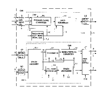
As can be seen in Figure 1, the device according to the invention comprises, in a
single integrated circuit chip IC, a transmitter TX and a receiver RX. Transmitter TX
receives through an input line 1 a parallel data stream and converts it into a serial stream
15 which is provided on output line 2. Via other input wires 3, 4 the transmitter receives
clock signals, whose frequency depends on the bit rate on line 2 and on the degree of
parallelism of the data stream, and a cell synchronism signal. Receiver RX performs the
opposite function: thus it receives serial data through an input line 5 and provides
parallel data on output line 6 and clock signals and cell synchronism signals on wires 7
2 0 and 8. RX also receives, through wire 9, a system clock signal to be used for
synchronism recovery.
By way of example, reference will be made to a bit rate of 311 MbiVs on line 2,
and therefore to a 77.8 MbiVs (4 bit parallelism) or 38.9 Mbit/s (8 bit parallelisrrJ) input bit
rate. The frequency of the input clock signal shall therefore be 77.8 MHz or respectively
38.9MHz.
A more detailed examination of the structure of transmitter TX shows that it
comprises, in addition to the actual parallel-to-series converter PS, a data scrambler SC
for line coding of the serial stream exiting PS and a circuit PL1 for generating the timing
signals for PS and SC.
3 0 Circuit PL1 is a circuit, advantageously based on a Phase-Locked Loop (PLL),
which multiplies by 4 or by 8 the frequency of the clock signal associated with the data in
order to generate, on wire 10, the fast timing signal (311 MHz) required to command the
operations of PS and SC. The structure of PL1 is wholly conventional.
Converter PS comprises, as can be seen in Figure 2, a conventional shift register
3 5 SH which loads either the data arriving over line 1 or, in the presence of the cell
synchronism pulse, a cell start (or synchronism) byte, read from an appropriate memory
MPS. For this purpose, between the cells of the shift register and memory MPS there is
a bank of multiplexers MX which have a first input connected to input line 1 and a second
2 1 9~69
input connected to MPS. The cell synchronism signal serves as a command for
positioning multiplexers MX on the second input and as a command for reading thesynchronism word. The synchronism word is chosen between two possible words suchas to have a limited overlapping range or even no overlapping range, and either word is
S loaded into SH at alternating cells. Advantageously, the two words can be
complementary to each other. In one exemplary embodiment, the two words are
respectively 0101001 1 and 10101100. The structure of a cyclically read memory is well
known to those skilled in the art.
If the circuit can be configured to handle streams with either 4 or 8 bit parallelism,
1 0 register SH also receives a configuration signal C48 which commands the positioning of
a second group of multiplexers M1...M7, internal to register SH, so as to establish the
alternation between loading the bits present at the outputs of the multiplexers of MX and
shifting the already loaded bits, required by the degree of parallelism. The configuration
of IC in order it can operate with either degree of parallelism is obtained by connecting a
15 pin of the integrated circuit to either of two voltages. Signal C48 is generated by an
appropriate circuit, not shown.
It should also be noted that, in the case of 4-bit parallelism, the cell synchronism
signal present on wire 4 will last two cycles of the input clock signal, since loading the
synchronism word requires two cycles.
2 0 Going back to Figure 1, data scrambler SC encodes the serial streams exiting PS
in such a way as to generate a signal which: has a number of transitions high enough to
allow bit synchronism recovery in reception, regardless of the statistic of the input signal;
lacks long sequences of consecutive O's or 1's which would prevent the rec~eiver from
operating properly in case of a d.c. decoupling, as in the case of optical connections; and
2 5 has a null average value, which is necessary in case of d.c. decoupling. Circuit SC can
be implemented, with advantage, as described in ITU-T recommendation G709,
according to which a pseudorandom sequence is generated by using the polynomial 1 +
X6 + X7 as a generator polynomial. Scrambler SC receives the fast clock signal as a
timing signal of its operations and the cell synchronism signal as a reset signal. The latter
3 0 signal operates in such a way as to let the cell start word go through unaltered.
Receiver RX comprises a synchronism recovery and data alignment device PL2,
which regenerates the fast and slow clock signals starting from the incoming serial stream,
synchronises the stream with the reconstructed fast clock signal and provides, through a
wire 11, the synchronised serial stream to a descrambler DS, followed by the series-to-
3 5 parallel converter SP, and to a circuit FD for recognising the cell start word in the datastream circuit FD is in turn followed by a circuit SY for recognising that cell synchronism
has actually been recovered.
2 i ~ 9
Block PL2, also based on a PLL circuit, can be the circuit described in the
aforementioned European patent application or the one described in European patent
application EP-A 0 732 830, also in the name of the Applicant. This second circuit
comprises a main phase locked loop, comprising a phase detector, a driven current
5 generator, a filter and a voltage controlled oscillator, and a secondary loop, which allows
the main loop to become locked by bringing the voltage controlled oscillator to oscillate at
a frequency close to the operating frequency. In the main loop, the phase detector
compares the phase of the data signal with that of a locally generated clock signal and
provides an error signal which, through the driven current generator and the filter,
1 0 continually controls the phase of the voltage controlled oscillator. The secondary loop in
turn comprises a phase detector, a threshold detector and a driven current generator,
which feeds said filter.
PL2 provides on a first output 11 the re-synchronised data stream and, on outputs
indicated in the whole by 12, the recovered fast (311 MHz) and slow (77.8 and/or 38.9
1 5 MHz) clock signals, which are supplied to the other blocks of RX. The slow signals are
also presented on output 8 of the receiver.
Descrambler DS and series-to-parallel converter SP are exactly complementary to
SC and respectively PS. Similarly to SC and PS, DS and SP will receive also a cell
synchronism signal, which is supplied by SY through a wire 13 and is generated as will
2 0 be seen further on. Clearly, if the circuit can be configured to operate with two degrees of
parallelism, SP also will have to receive configuration signal C48.
Circuit FD is a simple decoding logic, timed by the fast clock signal emitted by PL2,
and aimed at recognising synchronism words in the data stream. Once recognition has
occurred, FD generates a signal indicating which of the two words has been recognised
2 5 and commands the execution, by circuit SY, of an algorithm verifying the regular
altemation, with cell rate, of the synchronism words. In steady state conditions (i.e. under
cell synchronism lock conditions), every time the correct synchronism word is recognised,
circuit SY sends the cell synchronism signal to DS and SP through wire 13, and emits the
same signal on wire 8 as well, with a delay equal to the operating time of DS and SP, so
3 0 that the signal on wire 8 is exactly aligned with the data.
Circuit SY essentially comprises a state machine, which executes the algorithm
shown by the state diagram depicted in Figure 3.
In this Figure, STF = 1 indicates that a synchronism word has been recognised;
FCODE = 0, FCODE = 1 indicate which of the two words has been recognised; FFA,
3 5 FFB indicate, when they are at 1, that word A or B, respectively, has been recognised
(so, they are two signals acting as logic AND of STF and of either FCODE signal); NTC
= 0 indicates the instant in which the arrival of a cell synchronism word is foreseen,
based on the clock signal count performed by an appropriate internal counter. C, A
- 2 1 9~69
indicate respectively the conditions that determine a transition and the actions carried out
during a transition. These are of no interest for the purpose of understanding the
invention and therefore shall not be examined in detail.
In particular, when STF becomes 1, SY passes from an initial state (IDLE) to one5 of the two synchronism pre-lock states (PRELOCK A, PRELOCK B), depending on
which word has been recognised. For instance, it is assumed that FCODE = 1 leads to
the state labelled as A and FCODE = 0 leads to state B, and that the first word
recognised is the one that leads to state A. The cell counter is also started, since the
following transitions occur with a cadence determined by the cell counter, in the instant in
10 which the synchronism word arrives or, if it does not arrive, in the instant in which it is
expected. From state PRELOCK A, SY goes to synchronism lock state (LOCK B) if the
other synchronism word is recognised (FFA = 1) after a cell period (NTC = 0). Under
these conditions the cell synchronism signal is generated. At the subsequent
synchronism word (which, if everything is operating properly, is the one that should lead
15 to state B and shall therefore be signalled by FFB = 1) SY goes to state LOCK B. The
operation is obviously analogous if the first synchronism word leads SY to statePRELOCK B. As long as the synchronism words alternate with cell rate, SY alternatively
goes from one to the other lock state, each time generating the cell synchronism signal.
If, due to a transmission error, one of the synchronism words is not received
2 0 correctly, SY moves on to an alarm state AL A ffrom LOCK B) or AL B (from LOCK A),
depending on the lock state it was in. In the next cycle, the system returns to the prelock
condition (always respecting the transition A -> B and vice versa) and then resumes the
normal cycle, if the synchronism is found, or returns to the idle state and re~starts the
verification cycle, if the synchronism is not recognised again.
2 5 For the sake of completeness the drawing also shows the permanence of SY in
each state (except for IDLE) between two instants of cell period end count.
Given the state diagram, the person skilled in the art has no problems in designing
the logic network implementing it.
Going back to Figure 1, the circuit also comprises inpuVoutput cells IP (parallel
3 0 input to the transmitter), US (serial output from the transmitter), ISD, ISC (inputs to the
receiver, for the serail data and the clock respectively), UP (parallel output from the
receiver) aimed at adapting the electrical characteristics of the signals present on the
external lines to those required inside integrated circuit IC and vice versa. According to
the invention, inpuVoutput cells related to the parallel stream can be chosen among cells
3 5 operating with different logic levels, according to the degree of parallelism and the
requirements of the system in which circuit IC is inserted. In case of 4 bit parallelism, cells
IP and UP can be chosen among differential cells operating with PECL logic levels (3.3 V
and 4.1 V for the low and high level, respectively) or single-ended cells operating with
- 21 9~9
RVS (Reduced Voltage Swing) levels, which use 0 V for the low level and 1.5 V for the
high level; in case of 8 bit parallelism, input cell IP can be a single-ended cell operating
with CMOS logic levels. The use of CMOS levels is not advantageous in the case of 4-
bit parallelism, where the various elements of the circuit must operate with clock signals
5 at a frequency of almost 80 MHz; obviously, the other types of cells can also be used
for 8-bit parallelism. For manufacturing reasons, cells operating with PECL levels will
advantageously be used only in a circuit destined to operate always with the same
degree of parallelism, whereas, in case of a configurable circuit, the same integrated circuit
chip may include both a cell operating with RVS levels and one operating with CMOS
1 0 levels, and the cell to be used may be selected by exploiting the same signal C48 which
configures the converters.
InpuVoutput cells US, ISD for serial data flow on the contrary are preferably
differential cells with PECL logic levels which on the one hand are well suited to the
required bit rates and on the other allow direct connection with circuits driving optical
15 components, which require these levels. Cell ISC associated with the system clock
signal can also be either a differential cell with PECL levels or a cell with RVS levels.
InpuVoutput cells operating with CMOS, PECL or RVS levels are well known to
those skilled in the art and do not require a detailed description.
The circuit just described overcomes the drawbacks of the prior art. In fact, the
2 0 alternation between two synchronism words, chosen with the criteria described above,
minimises the possibility of false synchronism locks. Moreover, the data scrambler
maintains unaltered the length of a coded bit sequence.
It is evident that what has been described is provided purely by w~ay of non
limiting example and that variations and modifications are possible without departing from
2 5 the scope of the invention. Thus, for instance, the parallelism considered may differ from
4/8-bit, or circuit PL2 could use a Delay-Locked Loop (DLL) circuit instead of a phase-
locked loop. The use of delay-locked loops to extract the synchronism from a data stream
is common in the art.