Note: Descriptions are shown in the official language in which they were submitted.
2 1 90459
~ W ogsl34977 P~
METHOD AND SWITCH NODE FOR SWITCHING STM CELLS
IN A CIRCUIT EMULATED ATM SWITCH
TECHNICAL EIELD
The present invention relates to a method o~ switching messages
divided into micro cells of variable length and to facilities
therefore.
sACKG~OUND A~T
EP-A1-528 085 relates to z combined ATM and STM network using
standard ATM cells a~ well as nDn-standard short cells ~or
transmission of information. Short cells are used in order to
reduce the p~rk~t;7ing time as well as~ythe depacketizing time. By
reducing the packetizing and depacketizing times the loop delay
is reduced thereby eliminating the need of echo cancelers.
Standard ATM cells, comprising 53 octets, are used whenever a
connection is set up from a STM switch to an ATM switch via an
intermediate ATM switch using standard ATM tr~n~ i nn proto-
cols. Short cells comprising a fraction, about 1/3, of the numberof octets of the standard ATM cell, is used whenever a connection
is set up between a STM switch and another STM switch via a ATM
switch so as to reduce the packetizing and depacketizing time of
the information cells within said latter, intermediate ATM
switch.
In this known system the transmission capacity, i.e. the band
width efficiency i.e the coefficient between the number of
octets of the header of the cell and the number of octets o~ the
payload of the cell is about 25% which is rather fair provided
all octets of the payload are used ~or information transfer. If
for example hal~ of the octets are~empty the packetizing and
depacketizing time will be the same, the bandwidth efficiency
will also be the same but the packetizing degree, i.e. ~uotient
of the number ~f octets of the header and the number of informa-
tion loaded octets of the payload, is reduced If small amountsof information are to be sent at irregular intervals, or if large
amounts of information are to:be sent at irregular intervals this
known device will provide a low packetization degree, which in
principle means-a bad use of the existing bandwidth.
2 1 9~4~
WO9sl34977 2 ~ c ~ ,~ o
DISCLOSURE OF THE INVENTION
The object of =the present invention is to prDvide a telP 1-
cation network and network entities with flexible cell size
adapting itself to the type of information to be~sent while
simultaneously providing small packetizing and depacketizing
delays, a high band width efficiency and optimum packetizing
degree.
Another ob~ection of the present invention is to provide a
telP~ In1cation system and system entities therefore allowing
the cell size to be changed during run-time.
Still another object of the invention is to provide a new
hierarchy of protocol layers including a physical route layer PR-
layer), a virtual path layer (VP-layer), a virtual channel layer
(VC-layer) and a circuit connection layer (CC-layer). The use of
a physical route layer in the protocol model wiil allow the use
of spatial ATM-switches switching at the physical route layer.
Still another=obJect of the invention is to reduce jitter of the
cells by providing a new method to put a number of VC-PDU-cells
in the VP-PDU part of a larger PR-PDU-cell. Said VC-PDU-cells
have either the same vlrtual path VP or, in case ATM-cells are
switched, the same virtual path and the same virtual connection.
Still another ob~ect of the invention ls to provide the tele-
;rntion system and system entities therein using switches
and mapping units supporting the protocol in accordance with the
invention.
These and other objects of the inventions will be described in
detail below in connection with the enclosed drawings.
BRIEF DESCRIPTION OF THE DRAWINGS
Figure l is a schematic view of a mixed ATM- and STM-
telPI ~ni cation network,
Figure 2 is a block diagram showing an ATM node in the mixed
network of Figure l,
21 90~5q
WO9s/34977 3 ~_"~
~igure 3 is a simplified timing diagram showing the circuit
emulation principlej
~igure54 is a block diagram showing the an ATM switch node
of Figure 1,
L
Figure 5 is used to explain micro- cell assembly and is
showing various wave forms and a time axis,
Figure:6 is s~Lowing a micro cell of a.first type in accor-
dance with the invention,
Figure 7 is showing a micro cell of a second type in accor-
dance with the invention,
Figure 8 is a time diagram showing the micro cells in aframe oriented manner,
Figure 9 is a diagram showing the layered protocol model in
accordance with the invention,
Figure 10 is a ~able showing the identifier AcS~I ~ of the
cells shown in Figure 11,
Figure 11 is a timing diagram showing micro cells in accor-
dance with the invention at the various network
entities shown in Figure 4,
Figure 12 is ti~e diagram used in ~YplAin1ng jitter of micro
cells at a switch entity shown in Figure 4,
Figure 13 i5 a~time diagram showing how the jitter of Figure
12 is reduced in accordance with the invention,
Figure 14A illustrates the general structure of a PR-PDU micro
cell at the physical route layer (PR-layer),
Figure 143 illustrates a further embodiment of the PR-PDU-cell
in Figure 14A,
2 1 9~459
W095l349?7 4
Figure 14C illustrates a PR-P~U-cell comprislng in its payLoad
a standard ATM-cell,
Figure 15 is showlng a VP-PDU-cell at the virtual path layer
(VP-layer),
Figure 16 is showing a VC-PDU-cell at the virtual channel
layer (VC-layer),
Figure 17 .is a block diagram showing an access unit in
accordance with the invention,
Figure 18 is a block diagram and a time axis used to illus-
trate how time slots are y~neLc~d on a frame
oriented basis,
Figure 19 is a block diagram showing the connection datarecord and control module~of Flgure 17,
Figure 20 is a diagram showing the time slot store, the
connection data record and control module and the
multiplexor of Figure 19 by which the cell header
and the cell payload portion are multipl~efl
together,
Figure 21 is showing a micro cell at the PR-layer,
~0 Figure 22 is showing the micro cell of Figure 21 at the VP-
layer,
Figure 23 is showing the micro cell of Figure 21 at the VC-
layer,
Figure 24A is showing a number of VC-PDU:s put in a PR-PDU-
cell,
Figure 24B is showing an ATM-cell in which a number of VC-
PDU:s have been put in its user data part, said
~ W095~4977 5 2 ~ 7 ~ P ~ s ~ - la
ATM-cell forming part of an PR-~DU-cell in accor-
dance with the invention,
Figure 25 is showing the larger cell of Figure 24A at VP-
layer,
Figure 26 is showing the cell of Figure 25 at the VC-layer,
Figure 27 is asimplified block diagram of the central switch
of Figure 4, in particular the means required to
support a spatial switch,
Figure 28 is a diagram showing the structure of the address
space used at each of the network entities of
Flgure 4,
Figure 29 is a diagram showing mapper unit MUl of Figure 4,
Figures - ~
30-32 is a flow diagram showing the operation of the
mapper unit of Figure 29,
Figure 33 is a diagram of mapper unit MU4 of Figure 4,
Figure 34 is a ~diagram showing the receiving portion of
access unit AU1 connected to access switch AS4 is
Figure 4, and
Figures
35,36 ls a flow diagram showing the operation of the
access unit of Figure 34.
DESCRIPTION OF ~:~ ~K~:~ EMs0DIMENTS OF T~ INVENTION
Standard TDM (Time Division Multiplex) switching re~uires that
timing information is carried implicitly with the time slots. In
particular the time slot position in the frame provides this
timing formation, i.e. the connection with which the time slot is
associated. The TDM techni~ue is used to carry delay sensitive
information, e.g. 64kbps (kilobit per second) digitized speech.
2 1 90~59
W095J34977 6 r.~
~or a 64 kbps rnnn~r~l on a time slot is transferred once every
125 ,us. The tlme interval of 125 ,us is referred to as a frame.
A new technique to carry information across a tel~ In;rntion
network is to use ATM (Asynchronous Transfer Mode) technique. The
ATM technique has a potential to~ utilize network resources
efficiently by allowing excessive and dynamically not used
bandwidth to be used in delay insensitive applications like data
communications. Another important benefit of ATM is that it
allows the building of compact and efficient switches at a
fraction of the hardware required for 5TM (Synchronous Transfer
Mode) switches. In the following description the term STM is
equal to TDM and will therefore be used. The ATM technigue is
also simpler because it requires no timing information.
Current ATM standards require that user data are put in cells
which contain up to 48 octets. An ATM-cell can be used to carry
time sensitive applications, such as for example speech. This
technique is referred to as circuit emulation on ATM. Circuit
emulation on ATM requires the STM timing information to be
restored at the ATM-network edges.
A standardized service supporting circult emulation is referred
to as AAL1 by CCITT. The AAL1 standard defines that 47 octets of
the payload of a cell comprising 48 octets be used for time
slots. If AAL1 is used to carry time slots of a 64 kbps connec-
tion it will cause a packetizing delay of about 6 ms (47-125,us).
This will add to a loop delay of 12 ms. The packetizing delay may
therefore require the use of echo cancelers. In mixed ATM and STM
networks echo cancelers must certainly be needed along voice
connections. At every transition from ATM to STM and from STM
back to ATM will cause an extra unpacking and packing respec-
tively with additional delays.
An evolutionary change of existing t~ nlcation networkswill most probably take place. A revolution with a rapid change
of today's networks towards ATM is probably not likely because of
the huge investments already made in existing STM technique.
2 1 90~ ~
W095/34977 7
The loop delay existing in ATM circuit emulation for 64 kbps
connections in a mixed ATM and STM network with repeated packing
and llnp~kin3 will most probably cause unacceptable delays from
a quality point of view.
In Figure 1 there is shown a mixed ATM and STM t~ ;cntion
network 1 comprising a number of ATM nodes 2 ar,d a number of STM
nodes 3. Each of the nodes 2 comprises an ATM switch and each of
the nodes 3 comprises an STM switch. The nodes 2, 3 are lnter-
connected by trunks represented by the indicated solid lines. To
each of the nodes 2, 3 a number of users are ~u~ ~L~d. In Figure
1 a user A having a telephone 4 and a data terminal 5 has access
to the network 1 at the ATM node 2 to the left, while a second
user B disposing of a tPl ~phnn~ has access to the same network at
the leftmost ATM node 2. The 6 ms delay caused by packetizing or
depacketizing at each ATM to STM transition has been indicated at
the upper STM node 3. If user A speaks over the phone with user
B the speech of user A will be delayed by 24 ms. In a big
network it is likely that several more transitions will occur
leading to unacceptable long delays.
Figure 2 is a block diagram showing the ATM node 2 of Figure 1 to
which user A is connected. Reference point "a" is an STM input
port receiving a number o~ time slots which are cyclically
repeated each 125 ,us, i.e. on a frame basis. Reference point "d"
is an STM output port transmitting the same time slots on a frame
basis. Reference points "a" and "d" have also been indicated in
Figure 1. The ATM node in Figure 2 comprises a swltch fabric 7,
a cell assembly unit 8 and a time slot restore unit 9.
Next, the circuit emulation princlple will be described with
reference to Figures 2 and 3. It is assumed that users A and B
are connected to.each other. Figure 3 is a 5implifi~ timing
diagram showing the circuit emulation principle with reference
to Figure 2. A first time axes 10 is iLlustrating the clock at
reference point "a" and time axes 11 is showing the clock at
reference point "d". The clock at "a" is not sy-luhLul-ized with
the clock at "b". The timing of the time slot at "a" is however
restored at re~erence point "d" as is illustrated by arrow 12
2 1 9~5~
WOg5/34977 8 I~l/a~ 15
shown in broken lines in Figure 2 and by the tlme axes 10, 11 in
Figure 3. Each interval T0, Tl, T2.... at time axes 10, 11
represents 125 ,us. During each such interval a predetermined
number of time slots are generated. This predetermined number is
the same from frame to frame. Each such time slot is~represented
by a small vertical mark. The time slots are numbered in
succession and are repeated on a frame basis. The circuit is
established between time slot 2 at reference point "a" and time
slot 5 at reference point "d". This circuit is represented by the
double headed, dashed arrow 13 in Figure 2. Each time slot number
2 at "a" is put in an STM-cell containing a virtual channel
number. The virtual channel is represented by doubled headed
arrow 14 in Figure 2. This is done in cell assembly unit 8. The
STM-cell is sent into the switch fabric 7 at reference point "b"
when the input line is free. The input line can be occupied by
other cells having other destinations. The STM cell is indicated
at 15 at reference point "b" in Figure 3. In the switch fabric 7
a virtual channel route is set up at circuit establi~' L. The
switch fabric unit 7 will then route the STM-cell 15 to the
reference point "c". All routing information are contained in the
STM-cell by means of the virtual channel number.
Inside the switch fabric 7 the STM-cell is transferred asynch-
ronously. This means that the time it takes the cell to Llav~
the switch fabric is dPrPn~nt on various pal. -L~l~ such as the
internal rate of the switch fabric, the traffic load of the
switch fabric. The STM-cell 15 leaves the switch fabric i at
reference point "c". The transfer time from point "b" to "c" may
vary from cell to cell belonging to the same connection due to
the above indicated parameters.
At reference point "c" the STM cell 15 has traversed~the switch
domain and the timing information of the time slot is restored by
the clock used at the time slot restore unit 9. Time slot number
2 is inserted in the time slot stre~am at the position of time
slot number 5 at reference point "d". The virtual channel is
associated to time slot 5 in a channel-to-circuit conversion
table not shown.
~ W09~34977 9 2 1 9 5 4 ~ L 5.'C /~
Since the STM-cell transfer time can vary the time slot restore
unit 9 must have a time slot buffer s~fficiently large to
accommodate the delay variation also referred to as jitter. If
not, loss of time slots can be expected. Cell delay is also
generatea at the input and output ports of the switch fabric 7,
i.e. at reference point "b" and "c" respectively. A separate
clock at time slot restore unit 9 is required to restore the time
slots at "d". There is, however, no need to carry frame synchro-
nization information in the cells. The clock is needed only to
provide time slot=synchronization so as to avoid loss of time
slots. It should be noted that between reference points "b" and
"c" cells are transported asynchronously without no timing
relation in relation to frames. The cells, however, comprises
time slots, each time slot being one octet.
In Figure 3 the time it takes to compose a cell 15 and to send it
away, is called the packetizing time, is indicated by the double
headed arrow 16 in the first frame T0-Tl, by the double headed
arrow 17 in the second frame Tl-T2 and by the double headed arrow
18 in the third frsme T2-T3. Since the switch fabric 7 is an ATM
type switch the cells will propagate through the switch fabric
asynchronously an will not arrive to the reference point "c"
regularly. Instead the cells 15 will arrive at reference point
"c" with various degrees of deIay, jitter, as ls schematically
indicated by the double headed arrows 19, 20 and 21 respectively.
It is important to provide sufficient buffering capacity in the
time slot restore unit 9 in order to maintain the order, with
respect to time, in which the cells arrive at the time slot
restore unit 9. A cell ~rom a previous frame must never be
~e~ ,-sed into time slots after the ~ s1tion of a cell from
a 5l~r~ in3 frame.
Accordingly, the time relationship between individual frames must
neve~ be reversed, This poses a problem which will be addressed
later on.
In Figure 4 the topology of an ATM switch node 2 is shown. The
node comprises four access swltches labeled ASl-AS4 and a central
2 1 90~5
W095/34977 lO r~ s
switch CSl. The interconnection between the access switches ASl-
AS4 and the central switch CSl are handled by mapper units MUl-
MU4. Each access switch comprises five access units-~AUl-AU5. To
each access unit telephone sets Tl-Tn, n = being an integer, are
connected. As an example access switch ASl is an extension module
ATM switch serving a building with gnn~ 'nlum apartments. The
number of access units, five in the illustrated example, is only
P~Pmpl~y and may vary from access switch to access~switch. The
number of telephone sets connected to an access unit may
typically be 24. The number of access switches connected to the
central switch, four in the illustrated example, is only
exemplary and may be different. Preferably the central switch CSl
is of the type described in my US patent application 08/011378
filed on January 29, 1993. A central controller 500 is supervis-
ing the traffic in the node and performs signalling in order toset up, or controls sign~lling units that set up, a connection
between two users, is supervising the traffic in the node and is
~Pc1~ing, on a run-time basis, the cell type and the cell size to
be used for an individual connection, said ~c1 e1 nn being based
on traffic analyses, user demand or other~ criterions such as
geographical position of a switch unit in the ATM-node.
In Figure 4 telephone set T5 at AU3 in ASl has est~hliehp~ a
circuit to t~lPphnnP set T4 in access unit AUl at AS4. A circuit
is depicted by the "hook off" tPlPrhnnP symbol. The circuit can
be defined as: ~
T5 x AU3 x ASl - T4 x AUl x AS4.
Moreover, telephone set T6 at AU4 at access switch ASl has
established a circuit to telephone set T8 at AUl at access switch
AS4. The circuit is depicted by the "hook off" shaded tPlPrhnnP
symbols. This circuit can be defined as:
T6 x AU4 x ASl - T8 x AUl x AS4.
Looking at the node topology model it is apparent that the two
circuits partly traverses the same distances.
Each access unit generates n time slots per frame, one time slot
being allocated to each of the tPl~rhnn~ sets Tl-Tn. Perhaps four
2 1 90~ 5q
WO95l34977 11 P~ a
different telephone sets are busy at the same time. The audlo
signal at each telephone set is sampled 8000 times per second. If
the quantisation distortion requires each sample to be housed in
8 bits, the bit rate must be 64 kbps. In accordance with standard
TDM switching a sample is transmitted each 125 us. Accordingly,
each sample is stored in the time slot and the time slot
comprises 8 bits, a so called octet. In the case of transferring
speech the bit rate is 64 kbps. In other applications, such as
data tr~n~miccinn, other higher bit streams are used. Indepen-
dently of which bit stream is used the time period of 125 us isreferred to as a frame.
In the exemplary ATM switch node of Figure 4 each access unit
generates n time slots per frame. Numbering the time slots in
order,-time slot T1 is allocated to telephone set T1, time slot
T2 to telephone set T2 etc.
If the switch fabric 7 has a standard ATM switch fabric the ATM
cell payload comprises 48 samples. Suppose only one t~l~phnn~ set
is busy and that the speech signal is sampled at each 125 ,us. It
would then take 48 x 125 ,us to fill, that is to packetize, the
ATM cell. As ~iccncs~ above such long paketizing time is
unacceptable in mixed ATM and STM networks. Still supposing
standard ATM cells are used and that only one t~l ~phnn~ set is
busy in a access unit one way to shorten the paketizing time
would be to send an ATM cell as soon as a sample has been taken,
thus ignoring to fill the following 47 samples. Accordingly 47
octets of the standard ATM cell would be transmitted empty. This
proposed solution is, however, unacceptable in view of the waste
of bandwidth since~the bit rate in this case would be 64 kbps x
53 = about 3.4 Mbps (provided that 53 time slots should be
transmitted each 125 us).
Accordingly there is a need to keep the packetizing time as short
as possible while simultaneously avoiding waste of bandwidth. If
the packetizing time is reduced the waste of bandwidth is
increased while on the other hand if the packetizing time is low
the bandwidth will be used r~ lly, In accordance with the
invention it is suggested that the number of time slots per cell
21 ~045~
W095/34977 12 r~ t ~ o
should be reduced from the 53 time slots of a standard ATM cell
to a any of the following s$zes: 4, B, 12, 16 and 20 octets. Such
short cells are referred to as micro cells. In ~r~nr~nm~ with
the inventlon, and for reasons explained in connection with
Figures 12 and 13, also larger cell sizes may be used, preferably
any of the following cell sizes: 56 and 60 octets. Such iarge
cells cannot be termed micro cells. As a common name for cells
having any of the listed sizes (4, 8, 12, 16, 20, 56 and 60
octets) are referred to as PR-PDU-cells. PR-PDU-cells of any of
these sizes, or combinations thereof, may be switched at the same
time through one and the same ATM-node 2~ In accordance with the
invention the cell size is get at the access units by the central
controller 500 and may be changed at a mapping unit so as to
comply with the above mentioned trade o~f between low packetizing
time and efficient bandwidth use.
In Figure 5 a micro cell C in accordance with the invention is
shown. The header of the cell comprises 4 octets and the payload
P of the cell comprises 4 time slots giving a micro cell size of
8 octets. Each long, thin vertical mark at the tlme axis
represents a frame and each small, thick vertical mark represents
a micro cell. Audio wave forms at telephone sets Tl, T3, T5 and
T7, which all belong to the same access unit, are shown in the
upper part of the Figure. The circles at the wave forms represent
different times at which samples of the speech are taken. In the
illustrated example 4 micro cells are sent at each 125 us. The
micro cells are numbered 1, 2, 3 and 4. Cell No. 1 belongs to
telephone set Tl, cell No. 2 to telephone set T3, cell No. 3 to
telephone set T5 and cell No. 4 to tel ~phon~ set T7. Since the
payload of each such micro cell comprises 4 time slots it takes
4 x 125 ~s to fill cell No. 1. Accordingly the packetizing tlme
is 0,5 ms. It will also take 0.5 ms to fill cell No. 2, cell No.
3 and cell No. 4. The added loop delay, compared to STM, will in
this case be 1 ms instead of 12 ms for ATM. The structure of cell
No. 1 is shown in Figure 6. The cell~has a header H and four time
slots in which four samples are stored. These samples belong to
one and the same telephone set Tl. Accordingly one cell carries
one connection. It will thus take 4 frames until the cell is
filled. In accordance with an alternative embodiment of the
~1 q'J4 5q
W095/34977 13 r~ c'~
invention shown in Figure 7 the tPIPrhnnP set T1 is allocated
time slot 1 in celI No . 1, telephone set T3 is allocated time
slot 2 in the same cell No. 1, tPlprhnnp set T5 is allocated time
slot T3 in the same cell No. 1, and tPl PrhnnP set T7 is allocated
time slot 4 in cell No. 1. In cell No. l in the next frame shown
in Figure 8 telephone set T1 is still allocated time slot T1,
telephone set T3 time slot 2, telephone set T5 time slot 3 and
telephone T7 time slot 4. The time slot order remains the same
from frame to frame. In this case 4 differe~t users are sharing
the same cell. This will shorten the packetizing time 4 times
compared to the embodiment shown in Figure 6. The loop delay will
accordingly be 4 times shorter, i.e. 250 ,us.
In order to reduce the packetizing time of micro cell No. 1 in
Figure 6 were it takes four frames to fill the micro cell it is
possible to transmit the micro cell as soon as the first sample
is received and let r~--i n ~ ng time slots be empty. This is shown
in Figure 8. This reduces the packetizing density and increases
the waste of bandwidth.
From the above it is apparent that the smaller the size of the
micro cell the shorter is the packetizing delay. However, the
smaller the cell size the less is the useful utilization of a
cell with regard to the length of the header. If the payload
comprises four times time slots (=4 octets) and the header is
four octets then only 50% of the cell is effectively used. In the
embodiment shown in Figure 8 only about 12% of the cell is
effectively used. This should be compared to a standard ATM cell
wherein about 90% is effectiv~ly used. Accordingly there is a
value in having larger cells at the same time as there is a value
in keeping the size of the payload small in order to reduce the
packetizing time. This is a reason why different cell sizes are
used in difierent parts of an ATM node 2 in accordance with the
invention. It is preferred to use the small cell size at the
access points to the ATM node while larger cell sizes are used in
the central ATM-node. The central controller 500 decides which
sizes that should be used.
2 1 9~4 ~q
WO95/34977 14
Taking the above ln consideration there is ~ trade_off be~ween
acceptable waste of bandwidth, effective utilization of the cell
and acceptable packetizing delays. The indicated ceLl lengths
used by the PR-PDU-cells in accordance with the invention
represent a fare CU~ 1 ce. ~ ~
In order to reduce delay caused by jitter a new protocol model,
bases on the same principle as the CCITm-OSI model regarding
interfaces between layer and peer to peer communications is
provided in accordance with the present invention. The CCITT-OSI
terms are used to describe the protocol in accordance with the
invention. To start with four distinct layers are l~Pnt~fi f~ in
the switch node shown in Figure 9 namely:
1. Physical route layer (PR-layer)
2. The virtual path layer (VP-layer)
3. The virtual channel layer ~VC-layer) ~ : ~
4. The circuit connection layer (CC-layer) that interfaces to the
user application.
Although Figure g is described in connection with telephone sets
it is apparent that other applications than telephony are
conceivable such as mobile trlfrhony, data trAnrmi csi ~n between
computers, video networks etc. So, instead of a tol ~ph~nf~ set the
more generic term user is used in the following.
The advantages with this layered model is that the lower layers
(the PR-layer~and VP-layer) can be set up more or less semi-
permanently. If this principle is used to its utmost a circuitcan be set up by operating only at the edges of the network. The
time required to establish a circuit from a ~-rAgf- t point of
view is thus reduced considerably.
An estAhl; ch~ circuit through all the layers is defined as a
circuit connection 24
Applying the layered architecture above and introducing the well
established definition of a Protocol Data Unit, PDU, for every
layer this will imply that an STM-cell comprises:
~ WO95l34977 2 1 9 0 4 5 9 PCT/SE9~0057~
1. A PR-PDU that is similar to the earlier defined STM-cell.
Note: the STM-cell has been redefined and is now a generic
term for an assembled cell.
2. A VP-PDU that is the user data of the PR-PDU
3. A VC-PDU that is the user data of the VP-PDU
4. A CC-PDU that is the user data of the VP-PDU or the VC-PDU.
The CC-PDU contains the time slot or=time slots_
The PR-, VP- and CC-layers are only valid within the switch node.
The CC-layer is the user data from the user of the node. The user
data are carried across the node.
The switch controlled PDUs has a Protocol Control Information PCI
and the user data. The PCI comprises essentially an identifier
which makes it possible assemble and disassemble the protocols.
A micro cell at various protocol layers will be ~c~r1 hP~ in
detail in Figures 21-26.
Next there will be described how time slots from t~l~rhnn~ set T5
~laV~L~S the ATM node 2 to telephone set T4 in accordance with
the protocol model above. This connection is the same as shown in
Figure 4.
The time slot coming from telephone set T5 in Figure 4 is given
to the access unit AU3. On top of the protocol stack in Figure 9
is the circuit connection layer 22. The user submits the time
slot as a SDU, Service Data Unit, to the VC-layer 23 Luy~heL
with interface control information specifying the clrcuit
connection 24 shown in dotted lines in Figure 9. In thls
particular case said infnrr~t~nn is the time slot number in the
frame, time slot 2.
The VC-layer 23 is not used in this particular case and is
therefore short-cut down to the VP-layer. The VC-layer represen-
3û tation is implicitly present in the VP-layer. The VP-layer in its
turn adds the VPI as PCI Protocol Control Information ana hands
21 9~5~
W095/34977 16 ~ 0
over the VP-SDU to the PR-layer together with interface control
information stating the physical route.
At the PR-layer AU3 adds the physical route identifier, PCI, and
transfers the protocol data unit (the cell) to the peer entity at
AS1. The ASl bridges the cell to the physical route indicated by
the physical route identifier PRI. The physical route identifier
is also changed from a trall termination sink identifier to a
trail termination source identifier.
At the peer to peer entitles in mapper unit MUl the procedures
are repeated in the reversed order with respect to access unit
AU3. At the VP-layer a bridging is made to the transmitting VC-
layer side. This VP-VC-bridging is illustrated by line segment 31
in Figure 9. The VC-layer attaches a VCI to the cell header and
passes the now created VC-PDU down to the VP-layer as an VP-SDU.
The same procedure as in the access unit AU3 is repeated, the VC-
PDU is encapsulated in the VP-layer and the VP-PDU is ~nr~psnlat-
ed in the PR-layer and the cell, now beiny an PR-PDU-cell, is now
sent to the central switch CSl.
At the central switch CSl a similar procedure as that in access
switch ASl is p~l' ~.
At mapper unit MU4 the only that takes place is a bridging at the
VP-layer. The 1n~ 1ng VPI and PRI uni~uely define the new
physical route. The VPI is normally changed but in this case it
remains the same VPI.
At the receiving access unit AU1 all layers are traversed up to
the user where only the time slot remains. The time slot is sent
to the t~l~rh~n~ set T4.
The other circuit connection T6-T8 shown in Figure 4 shares the
same VP-PDU between mapper unit MU1 and access unit AUl. It is
possible to do so since they share the same virtual path VP.
As shown in Figure 9 some system entities only bridges data. In
order to distinguish a termination point at which the SDU is
21 9~4~J9
~O9S/34977 17 r ~
transferred to or irom the ad~acent higher layer from a bridging
polnt the terms "trail'' and "link" connections (LC) are used.
This terms are defined in the CCITT G803 standard.
A trail is set up between two termination points, the source and
the sink. A trail consists of one or more link connections.
Identifiers are assigned to the PDU:s traversing a link connec-
tion The identifiers make it possible to associate the PDU:s to
their respective trails
In Figure 10 there is s~own a table containing identifiers which
are ~csign~ to cells traversing the node in Figure 4 for the two
connections shown in said Figure. The table shown in Figure 10
are used by the mapping units MUl-MU4 to translate the PRI, VPI
and VCI identifiers indicated in the header of an incoming cell
to new PRI, VPI and VCI identifiers which are put in the header
of the outgoing cells at a specific mapper unit. The identifier
assignment table in Figure 10 is set up by the control system 500
in accordance with generally known principles, In the example VC-
PDU are used for the AU3-MUl and the AU4-MUl connections. It is
possible to do SD thanks to the protocol model since the VC-layer
can be omitted and instead the PR- and VP-layers are used. It
should be noted, however, that lt would have been poccihlp to
assign VC-PDUs with associated VCIs.
From the VPI column in the table it is apparent that the same
VPI, that is VPI=~, is used for the two link connections T5-T4
and T6-T8. It is pnss~hle to do so when passing the SDU to the VP
layer since the other connection qll~l;fi~rQ, VPI and PRI, are
different. One could equally well have ~qcisn~ different VPIs
for the two connections and refraine~ from using the physical
route identifier PRI. However, by using the physical route
identifier PRI as a part of the identification the virtual path
identifier VPI and virtual connection identifier VCI can have
local administration with the same scope as the physical route.
Such local ~min~tration means that only parts oi the conversion
table shown in Figure 10 need to be used at the mapping units.
Accordingly, it is not necessary that each mapping unit comprises
~ 1 9~
W095l34977 18
the complete mapping table of all connections as set up by the
control system 500. This will be explained in more detail with
reference to Figures 28, 2g and 33.
However, there must always exist one significant identifier or a
combination of significant identifier in 'oraer to identify'the
connection or the trail at a higher layer. The significant
identifiers are marked in bold in the table in the example shown.
Of course, the example shown in Figures 4 and 10 only refers to
two connections. It may be difficult to understand the benefits
by the invention by just considering these two connections.
However, when considering that thousands of connections are busy
at the same time it is easy to understand that it will be easy to
find a uni~ue combination of identifiers for each link connec-
tion.
In Figure 11 the PR-PDU-cells making up the two connections shown
in Figure 4 are shown when traversing the ATM no e of Figure 4
from their originating access units AU3 and AU4 to their common
terminating access unit AU1. In Figure 11 three time axes 25, 26
and 27 are shown. Time axis 25 represents the time at access
unit AU3, time axis 26 represents the time at access unit AU4 and
time axis 27 represents the time at the terminating access unit
AU1. The vertical marks T0, T1, T3.... represent times that are
separated by 125 ,us. Figure 11 is rather complex but tries to
give the essence of the STM switching principle. The time slot
TS#5 for the CC-trail T5-T4, denoted 24 in Figure 9, is put in a
small PR-PDU-cell at every frame generated at access unit AU3.
These small PR-PDU-cells are denoted 28/1, 28/2, 28/3... and are
generated during the first, second and third frame respectively.
When travelling from AU3 to AS1~ PR-PDU-cell 28~1 has the
indicated PRI and VPI identifiers PRI#1 and VPI#1. The mapper
unit MU1 changes the PRI# from 1 to 2 when the small PR-PDU-cell
28/1 leaves ASl. The VPI remains unchanged. In a similar way the
time slot TS#6 is packed into PR-PDU-cells 29/1, 29/2, 29~3... at
each frame generated at access unit AU3. The small PR-PDU-cell
proceeds from AU3 to ASl and has during this journey a PRI equal
~ 1 90459
W095/34977 19 l~ a
to 1 and a VPI equal to 1. When arriving to access AS1 the PRI is
changed from l to 3 as indicated at PR-PDU-cell 29'/l, 29'/2,..
At mapper unit MU1 a VC-PCU is created for time slat TS#5 and
another VC-PCU is created for time slot T#6. The two VC-PDU:s are
both put into the user data of a VP-PDU-cell, which in accordance
with the example has a VP-trail common to the two VC-links. The
VP-PDU-cell with the two VC-PDUS:s in its turn is put in a new
large PR-PDU-cell 30/1. A VC-PDU is accordingly created for each
time slot. In this particular case VCI#1 is ~cq1gn~ to time slot
TS#5 and VCI#2 is assigned to time slot TS#6. This VC-PDU packing
procedure is repeated at each frame interval as indicated at PR-
PDU-cells 30/2 and 30/3
From the protocol layers shown at MU1 in Figure 9 it is apparent
that a VC-PDU should be added to the PR- and VP-layers. In Figure
9 this has been indicated by line segment 31 bridging the VP- and
VC- layers. In accordance with the invention the VC-PDU:s are not
put into the header 32 of the PR-PDU-cell 30 but in its payload
33. It is possible to do so since a VCI identifies the time slot
it is carrying. In PR-PDU-cells 30/l, 30/2... the time slots TS#5
and TS#6 appear in reversed order. This depends on the fact that
time slot TS#6 arrived at mapper unit MU1 prior to time slot
TS#5. The arrival time of a cell can vary depending on other
traffic in the ATM node. Such varying arriving times are
characteristic ior an asynchronous ATM-switch. By generating the
VC-PDUs and by putting the VC-PDUs in a VC-PDU which then is put
in a PR-PDU-cell immediately at time at which the ~ e~Live time
slots TS#6 and TS#5 arrive at MU1 the time delay for the two time
slots at MU1 is reduced as will be explained later on. To put two
or more VC-PDU:s in the VP-PDU user data of one common PR-PDU-
cell is in the following referred to as connection of the two ormore VC-PDU:s.
From mapper unit MU1 the PR-PDU-cell 30~1 propagates to the far
end AU4 with only minor re-mapping. In particular the PR-PDU-cell
30 arrives to the central switch CS1 wherein its PRI is changed
from PRI=l to PRI=2_ This has been indicated in bold in Figure 11
at the PR-PDU-cell 30'/l. The prim sign indicates that the PR-
2~ 90459
W095/34977 20 P~ /a
PDU-ceLl is the same as the PR-PDU-cell 30. The PR-PDU-cell 30'
propagates to mapping unit MU4 and at MU4 the PRI is changed from
PRI=2 to PRI=l in order to get a local asslgnment of the virtual
path identifiers. The PR-PDU-cell is now denoted 30''/1 in Figure
ll. The physical route identifier is changed from PRI=l to PRI=2
when the PR-PDU-cell 30'' leaves the access switch AS4 on its
route to the terminating access unit AUl. When arriving to AUl
the PR-PDU-cell is denoted 30''' its PRI is changed from PRI=1 to
PRI=2. At access unit AUl the PR-PDU-cell 30''' is ~isAl ~ 1P~
and the indivldual time slots TS#6 and TS#5 are put ln the frame
oriented bit stream generated at access unLt AU1. In particular
time slot TS#6 is put into the time slot as agreed upon at the
set up of the CC-trail. Accordlngly time slot T#5 in 30''' is put
into the time slot ~ss~gnP~ to telephone set T4 and time slot
TS#4 is put into the time slot assigned to telephone set T8 as
indicated by arrows 34 and 35 respectively. This procedure is
repeated cyclically on a frame basis at access unit AU1.
Figure 11 is somewhat simplified in that the small PR-PDU-cells
28 and 29 are shown to contai~ only one time slot in the payload.
The cell is delivered as soon as ~ts time slot is filled with
user data. As Pxpl~nP~ ln connection with Figure 5 the size of
the payload of a cell is determined by the central controller 500
at call setup. Based on traffic analyses at each of the access
units the controller 500 may find that several connection should
be carried by one and the same cell, like in Figure 7, and the
controller will then select the proper cell type and cell size.
How this is done is described in connection with Figure 19.
Anyway Figure ll shows that PR-PDU-cells of different cell sizes
are used, in particular PR-PDU-cells 28 and 29 have one cell size
while PR-PDU-cells 30 has another, larger cell size, in this
particular case the sum of the sizes of the VC-PDU:s of cells 29
and 30.
Figure 11 also illustrates the important aspect of the present
invention, namely the use of VC-PDUs as VP-PDU user data in the
user data of the VP-PDU-cell. The VC-PDU is generally comprising
a virtual circuit identifier VCI and user data. The user data in
2 1 ~04 59
W095/34977 21 r ~ c
this particular application comprising one or more time slots in
a pre-arranged and pre-determined order.
The VC-PDUs are created inside the ATM node 2 as described in
connection with Figure 9 or can be created at the access nodes
~ep~n~ng of the current situation. To create nnn~ccary VC-PDUs
costs extra bandwidth.
The use of VC-PDUs provides a tool for3perfoFming a~y,l~hl~..ous
mapping. Asynchronous mapping is made in order to reduce the
propagation delay of a cell. Two mapping methods can be applied,
one using asynchronous VC-PDUs and the other not using any VC-
PDUs. There is a trade off between the two methods. Mapping
without VC-PDUs minimize waste of bandwidth but increases delay
while mapping by using VC-PDUs reduces delay but increases
bandwidth neea. =~
For booth methods the following common prere~uislte apply: At a
mappeF unit, for example MUl, a number of virtual paths VPs are
terminated. An ~ n: i ng PR-PDU belonging to a virtual path VP
holds one time sIot. The PR-PDUs, each belonging to an indivldual
vlrtual path VP, arrlve at random - in respect to time - to the
mapper unit. All PR-PDU-cells will therefore arrive withln a
irame lnterval but the order in which the PR-PDU-cells arrive may
vary from frame interval to irame interval.
It should be noted that the frame has no real signiflcance since
internally the node is asynchronous. The frame is only used in
order to indlcate the regularity of the time slots at the
perlphery of the ATM node and to indicate the regularity by which
the PR-PDU-cells are dispatched at an originatlng access unit.
In the example of Flgure 4 all time slots b~lnnging to different
virtual paths are routed to one single outgoing virtual path
traverslng the same section to the next VP-VC terminatlng entity
AU2. The reason for using this virtual path is to reduce overhead
(cell administration related data) whlle maintaining a low delay.
A common PR-PDU-cell header 32 is namely used for many time
slots, 2 time slots in the example.
21 90~59
W095/34977 22 P~ O
If no VC-PDUs are used: The VP-PDU user data part of the PR-PDU-
cell will contain just time slots and these must be all~ny~d in
a predetermined order.~If the order~ln which the time slots are
arranged is reversed, changed or otherwise upset, the origln of
each time slot is lost. If the origln is lost then it 15 not
possible to connect an originating user with its proper terminat-
ing user. Because the payload only comprises time slots the PR-
PDU-cell cannot be dispatched until all time slots making up the
cell have arrived. If the PR-PDU-cell, like PR-PDU-cell 30 in
Figure ll, is composea by two or more small PR-PDU-cells, the
large PR-PDU-cell 30 canno=t be dispatched until the last small
PR-PDU-cell, for example PR-PDU-cell 28', containing one or more
time slots, has arrived. Since the small PR-PDU-cells arrlve
randomly, due to the asynchronous nature of the switch and due to
lS the switch behavior, the waiting time for the large PR-PDU-cell
30 is indefinite but will at least be shorter than a frame
interval. On the other hand, the payload of the o hi nP~ large
PR-PDU-cell is fully utilized.
If VC-PDUs are used: In this case a virtual connection identifier
VCI is attached to the time slots of an i n~ 1 ng VP-PDU and will
thus form a VC-PDU. The VCI and the time slot or~time slots
attached to it is put in the payload of a large PR-PDU-cell or
even in the payload of ATM-cell. In the following the VCI and its
attached time slot or time slots is now referred to as a VC-PDU
and this VC-~DU is now an ln~r~n~nt unit that can be put
anywhere in the outgoing PR-PDU-cell. The outgoing large PR-PDU-
cell can be dispatched as soon at it is filled or as soon as a
certain predetermined amount of time has lapsed. After such
dispatching has taken place a new PR-PDU-cell b~lmn91ng to the
same virtual path is ready for a new set of VC-PDUs. In this way
the PR-PDU-cells will be dispatched as soon as they are filled or
will be dispatched at regular time intervals irrespective of the
level to which its payload has been filled. If the PR-PDU-cell is
dispatched at regular intervals it is possible to determine the
size of the cell at the time it is dispatched. On the other hand
if the PR-PDU-cell is dispatched only when it has been filled a
predet~rmln~ cell size can be used. This method with VC-PDUs in
the payload reduces the waiting time and therefore the delay. If
~ W09~34977 23 ~l 9 0 ~ ~ ~ r~ r ~
the number of incoming time slots is larger or much larger than
the number of VC-PDUs in the outgoing PR-PDU-cell it is preferred
to use large PR-PDU-cells comprising 56 or 60 octets.
The two methods described above are illustrated in Figures 12 and
13. An In~ lng PR-PDU-cell stream arriving to a mapper unit, for
example MUl, is denoted 36 in Figure 12 and 37 i Figure 13. In
both streams PR-PDU-cells from different virtual paths make up
the illustrated bit stream. At the mapper unit the individual PR-
PDU-cells should be organlzed into an outgoing cell that could be
a large PR-PDU-cell or an ATM-cell, in other words a PR-PDU-cell
of suitable size. This PR-PDU-cell is denoted 38', 38'' in Figure
12 and 39', 39'' i Figure 13. If no VC-PDU:s are used in the
payload of the PR-PDU-cells 36 it will be ner~qc~ry to collect
the payloads of cells from virtual paths into the PR-PDU-cell 38'
in a predefined order. Such collection takes time. The time slots
arrive in a random order to the mapper unit. They must be put in
8 predetermined order in the waltlng outgolng PR-PDU-cell. In
other words the time slots must be sorted into their predeter-
mined posltlons in the walting PR-PDU-cell. The waiting cell
cannot be dispatched until all time slots have been put in their
respectlve positlons. Jn addltlon, such collection time varies
from one waiting cell to the next. Therefore the outgoing PR-PDU-
cells are dispatched irregularly. This is referred to as jitter
When the PR-PDU-cell 38' has been filled it is delivered and the
procedure is repeated, i.e. the payload (= time slots) in cells
from virtual paths are collected in one and the same PR-PDU-cell
which, when filled, is dispatched. Accordingly, each PR-PDU-cell
38', 38''. ~ is dispatched with an undefined delay, illustrated
by the two double headed arrows 40 and 41 respectively. The
waiting time for a PR-PDU-cell 38 at the mapper unit is in
principle independeht of the size of the PR-PDU-cell 38.
Figure 13 illustrates the case when the payload of the PR-PDU-
cells 37 comprise a VC-PDU. A VC-PDU comprises VCI and CC user
data (time slots). In this case the mapper unit does not need to
sort the payloads of 1 n~ lng PR-PDU-cells in a predetermined
order in the outgoing PR-PDU-cells. Instead the mapper unlt reads
the virtual path in the header of each inl ing PR-PDU-cell,
2 1 90~5~
WO9~/34977 24 1~l _5 '
reads its destination, indicated by the virtual path identifier,
and collects the payload of alI cclls having one and the same
virtual path as destination into the larger PR-PDU-cell 39'.=When
the larger PR-PDU-cell 39' is filled it is dispatched. The mapper
unit will in this case immediately map the VC-PDU of an ~nl in3
PR-PDU-cell into the waiting PR-PDU-cell 39'. Accordingly the
delay is r~nc~nably r~educed. The delay or~waiting time will in
this case depend on the size of the PR-PDU-cell_ The smaller the
size of a PR-PDU-cell is the shorter is the delay.
Figure 14A illustrates the PR-PDU in the header of a PR-PDU-cell
in accordance with the invention. The PR-PDU is divided into a
PR-PCI part and a PR user data part PR-SDU. The PR-PCI part
contains the following fields: A first field 42 comprising the
physical route identifier PRI, a second field 43 comprising a
cell format indicator CFI and a third field 44, comprising a
priority bit. The PRI-field 42 comprises 5 bits.
The cell format indicator, CFI, 43 can take the values of O and
1. Format indicator 0 indicates a payload comprising 3 octets
(time slots). Format indicator 1 indicates that the next
following octet (octet 2 in Figure 14A) belongs to the cell
header and that it comprises the four fields M, CTF, FREE and SBP
shown in Figure 14B.
In Figure I4B field M takes one bit which is used for indicating
if multicasting of the PR-PDU-cell is completed or not. Field CTF
takes 4 bits which are used to indicate the slze of the payload
of the cell in accordance with the following coding (decimal):
CTFTOTAL CELL SIZEPAYLOAD
1 8 6
2 12 10
3 16 14
4 20 18
56 53 ATM-cell is switched
6 60 53 ATM-cell is switched
~ WO9S/34977 25 2 i 90~59 P~l c~
The SBP bit of Figure 14B is a parity bit. The bit in the FREE
field may be use~d for different purposes, such as indicating the
service class in case an ATM-cell is switched.
In Figure 14C the general layout of a PR-PDU cell comprising in
its payload a stan~dard ATM-cell which in turn comprises the
conventional 53 octets. Since the cell containing the ATM-cell is
a large cell it w~ll not be referred to as a micro cell. Instead
it will be referred to as a PR-PDU-cell_ As ~rl~i n~ previously
the term PR-PDU-cell also comprises micro-cells at the PR-layer.
In Figure 15 the structure of the VP-PDU of a cell at the VP
layer in accordance with the invention is illustrated. The VP-PDU
is divided into a VP-PCI part and a user data part VP-SDU. The
VP-PCI comprises the following fields: A first field 46 contain-
ing the virtual path identifier, VPI and a second field 47
comprising a parity bit relating to the VPI field 46. The first
field 46 comprises 7 bits. The first and second fields 46, 47
together make up an octet. In the VP-SDU-part, labelled 48, user
data comprising 2, 5, 9, 13 or 17 octets are stored. The size is
implicit det~rminP~ by the PR-SDU size. The VP-PDU sizes will
therefore be 3, 6, 10, 14 and 18.
The Virtual Path Identifier (VPI) in field 46 ranges from 0-127.
The VPI:s are ~cq~gn~d from a low value and in sequential order.
The following VPI range map apply:
0-1 reserved for r n~g~ t
2-127 valid user numbers
The virtual channel identifier, VCI, in field 49 ranges from 0-
127. The VCI:s are assigned from a low value and in se~uential
order. The following VCI range map apply:
0-1 reserved for management
2-126 v-a1id user numbers
127 indicates dummy VC-PDU, contains no useful
payload.
In Figure 16 the structure of a VC-PDU-cell is shown. The VC-PDU
is divided into a VC-PCI part and a VC-SDU part. The VC-PCI part
21 qO~5q
W095~34977 26 r~ o
comprises a first field 49 containing the Virtual Channel
Identifier (VCI) and a second field 50 comprising a parity bit
relating to the VCI. The first and second fields 49, 50 together
make up an octet. In the VC-SDU part, labelled 51, user data
comprising 1, 4, 8, 12 or 16 octets are stored. The user data can
be of any size as long as it can fit into the PR-PDU-cell. For
the defined PR-PDU-cells the following user data sizes are
defined: 1, 4, 8, 12 and 16 bytes. The size is implicit by the
PRI size in the PR-PDU-cell and in the assigned VP r.~nnP~tl nn
The entire VC-PDU can be put in the VC-PDU user data or in the
ATM-cell payload toge~her with other VC-PDU:s. In the later case
the VC-PDU can be of any suitable size.
Figure 17 is a block diagram of an access unit shown in FIgure 4,
for example access unit AU1. The access unit comprises a A/D
converter 54 a time slot counter 55, a time slot store 56, a
connection and control module 57 and a cell assembly multiplexor
S8. The access unit encapsulates the time slots in a PR-PDU-cell
according to the circuit emulation principles described above.
Tnl 1 ng time slots can be stored as VP-PDU user data in the PR-
PDU-cell in any combination. A group of time slots or a single
time slot can be put in a PR-PDU-cell. The cell size~is selected
in accordance with the number of time slots which are to be put
in the payload of the PR-PDU-cell.cThis is done by the central
control unit 500 The user data can also be mixed up with VC-
PDU:s as indicated in Figure 16.
Figure 18 is a detailed block diagram showing the A/D converter
in Figure 17. Subscriber lines 58, each one ~ul...e~Led to a
respective subscriber T1-Tn, is connected to a respective
analog/digital converter 59 which converts speech into di~ital
form. The A/D converter 59 takes a sample of the speech signal
each 125 us and stores the sample in a register 60. The digitized
value of the sample is transferred into a parallel to serial
register 61. At each respective parallel to serial register 61
there is present, during each 125,us interval a sample comprising
8 bits. Each register 61 has an output connected to a multiplexor
62 multiplexing the n audio~signals in a stritly timed order
~ W095/3497~ 27 2 1 9 0 4 5 9 P~ C la
onto an output line 63 ~rom the A/D converter 54. The multiplexor
62 may conceptionally ~e thought of as comprising an rotating arm
64 C~nn~ng each of the outputs from the registers 61. Assuming
one sample is contained in one octet that comprises 8 bits and
~ss- ; ng one sample i5 taken each 125 us the arm 64 is rotating
at a rate of 512 Khz giving a time slot stream rate of 64 kbps.
The order in which the outputs of the registers 61 is scanned is
never changed. The digitized sample of t~l ~phnn~ set Tl is put in
time slot #1, the sample from t~l~rh~n~ set T2 is put in time
slot #2, the sample from t~l~rhone set T3 is put in time slot #3
etc up to the last sample from telephone unit Tn which is put in
time slot T#n. This procedure is repeated during the next 125 ,us
interval as shown at the bottom of Figure 18. Each time slot
shown in Figure 18 thus represents n bits. Arrow 65 in Figure 18
represents a clock signal keeping track of the time at which each
register 60 takes lts sample. At tel ~phone set T1 this time
occurs at one and the same time within each successive 125 ,us
interval. At t~l ~phone set Tl this occurs at time slot TS#l, at
telephone set T2 this occurs at time slot TS#2 etc as shown in
Figure 18. The time slot stream from the A/D converter is stored
in a time slot memory 56. Each time slot TS#l, TS#2 ... TS#n is
stored at a position corresponding to its number in the frame.
The position in the time slot store is write addressed by the
time slot counter 55 which increments one step for each new time
slot. The time slot counter starts from zero when a new frame
starts. If time slots from more than one frame are to be put in
the cell (c.f. Figure 7) a multi-frame counter is used. The size
of the time slot counter and of the time slot store equals the
number of time slots in the i n~ 1 ng time slot stream.
The time slot store 56 comprises a number of locations, each one
associated with a cell quali~ier 66 and an index address 67. This
has been indicated in Figure 19~ The connection and control
module 57 holds a description of the PR-PDU-cell. The cell
description comprises a cell header 68 and a read address 69. The
read address indicates the address in the time slot store 56 at
which the time slot to be put in the VP-PDU user data should be
fetched. If the user data contains VP-PDUs the virtual channel
2 1 904 5~
W095/34977 28 ~ = p~ h~c~ a o
identifier VCI is also found in the~connection control module 57,
The cell qualifier 66:indicates if:the time slot is to be put in
the VP-PDU-cell user data part or not. In the case of the example
of Figure 4 the time slots belonging to telephone sets T5 and T6
should be put in the VP-PDU-cell user data-part while the time
slots belonging to the rest of the shown t~l ~ph~n~ sets should
not qualify for insertion.
The connection control module 57 is addressed~by ~he time slot
counter 55 in order to establish a relation between the PR-PDU-
cell and the time slot. Connection and control module 57 controlsthe cell assembly multiplexor 58 that assembles the PR-PDU-cells.
This cell assembly multiplexor 58 also comprises means for
generating parity 3 and a bit interleaved parity in the VP-PCI.
Parity l and parity 2 in the PR-PCI~are pre-calculated and stored
directly in the connection data record.
In Figure l9 a block diagram cf the GonnectiDn and control module
57 is shown. A connection data record 70 comprises an index table
71 and a cell descrIption table 72 which in turn comprises a
number of locations 73 of which one is shown in Figure 19. The
connection and control module 54 further comprises que means 74
for queuing incoming index addresses, a cell address counter 75
and sequence update means 76. There is also a qualify decoaer 77
controlling the operation of a multiplexor 78.
Next the operation of the connection and control module 57 will
be described with reference to Figure 20. The time slots
generated by the A/D ~IIV~L ~r,54 should be assembled into a
micro cell. The time slots are stored in the time slot store 56
under control from the time slot counter 55. If the cell
qualifier equals 0 this indicates that more time slots are to be
stored before the PR-PDU-cell is delivered. If the cell qualifier
66 equals l this indicates that the PR-PDU-cell has been filled
and is ready for delivery. If the PR-PDU-cell comprises just one
time slot then the PR-PDU-cell comprising this time slot should
be delivered a soon as a time slot has been stored in the time
slot store. If a PR-PDU-cell comprises more than one time slot
the cell qualifier 66 is used to indicate when the last time slot
~ W095l34977 29 2~90459 r~
of the PR-PDU-cell has been written into the time store 55. The
time slot store 56 also comprises an index address table 67
comprislng a number of locations, each location corr~cpon~1ng to
a respective time slot. The index address location ccrrDcp~n~i ng
to the last time slot of the pR-pDu-cell comprises an index
address to the index table 71 at which address a pointer to the
address of the cell start in the cell~description table 72 is
stored. In the cell description table 72 pointers~ to the cell
descriptors 73 are stored The number of cell descriptors equals
the number of virtual paths that are supported by the access
unit. The celL descriptor 73 has the same size as the size of a
PR-PDU-cell. The cell descriptor 73 i5 an image of the PR-PDU-
cell itself with memory locations for the cell header 68 and the
VP-PDU user data. However, user data are not contained in the
cell descriptor 73. Instead pointers to the time slots making up
such user data are stored therein The pointers point to the
addresses in the time slot store where the digitized values
making up an individual time slot are stored. In this way the
cell descriptor fs generlc for all PR-PDU-cells sent in succes-
slve frames. However, the cell descriptor are dlfferent fordifferent PR-PDU-cell sizes. In the shown example cell descriptor
73 comprises a cell header 68 and four pointers of which pointer
*TS1 points to the location of TS#1 in time slot 56, pointer *TS2
points to the address of TS#2 in time slot 56 etc. Since four
virtual paths are conceivable four such cell descriptors 73 are
shown, each such descriptor being related to a respective virtual
path. The cell descriptor comprises a control gn~l;fiPr 79 which
indicates if the cell descriptor data relates to the cell header
or to the payload. In the former case the control qualifier
eguals 1, in the latter case the contror qualifier equals 0. This
information is decoded in the gualifier decoder 77 controlling
the multiplexor 78
Generally the cell~~assembly process follows the fQllowing steps:
Samples from successive frames are stored in the time slot store
56 until the last time slot of the PR-PDU-cell is filled. When
the last time slot has been filled this is indicated by setting
cell gualifier 66 to 1. The corresponding cell descriptor 73 is
taken using the index address in the time slot store 56. It is
21 93459
WO9Sl34977 30 ~
now time to deliver the PR-PDU-cell The delivery is controlled
by the cell assembly multiplexor 58 which is controlled by the
control qualifier 79 As long as a control gualifier 79 equals 1
the arm 80 of the multiplexor is in the upper position shown in
Figures 17 and 20 and the cell header 68 is put into the outgoing
cell stream 81. When the control gualifier 79 switches to a 0
contents of the cell descriptor pointers 69 are swapped with
contents of the corresponding time slot store locations thus
outputting the corresponding time slots into the cell stream 81
immediately after the header. In this manner cells are generated
at a frequency which is controlled by the internal clock signal
65. The index table 71 is used to organize the cell descriptors
and provides a means for finding the cell to be delivered. As
indicated in Figure 20 _ different cells, each one corresponding
to a respective virtual path, is conceivable. The index table
contains the address to the cell to be delivered. Cell delivery
is asynchronous. Suppose a PR-PDU-cell is under its way being
delivered and that a number of time~slots accordingly should be
outputted. While this takes place the first time slot of a
following cell ls en~ered into the time slot store~ The index
address of this cell is now queue~d in the queue means 74, a
memory of the type first in first out. Accordingly the next cell
has to wait until the last time slot of the preceding cell has
been delivered. Not until the last time slot of the preceding
cell has been delivered the arm 80 of the cell assembly multiple-
xor 58 is returned to its upper position and the cell header of
the next cell, pointed to by the index address stored in the
queue means is delivered.
The cell address counter 75 starts to count at the start address
of a cell header, said start address being indicated in the cell
description table 72. The cell address counter then counts each
position of the cell descriptor while the cell i5 being outputted
into the cell stream While performing this counting the cell
address counter 75 monitors the cell qualifier 66 When the cell
qualifier 66 equals 1 the cell address counter 75 stops counting
and reverts to the queue means 74 in order to fetch the index
address of the next cell. Accordingly the size oi' the cell is not
stored in the cell counter 75. Further to controlling the cell
.. _ . . . . . . .
~ w095~4977 31 21~D~
assembly the control qualifiers 7~ in the cell descriptor 73 has
the following functions:
l Cell header octets #1 to cell assembly ~multiplexor 58.
Increment cell address counter 75.
2. Cell header octet #2 to cell assembly multiplexor 58. Write
back updated sequence number Increment cell address counter.
3 Cell~header octet #3 to cell assembly multiplexor. Insert
generated parity 3. Increment cell address counter 75
4. Virtual channel and sequence number to cell assembly multiple-
xor 58. Write back updated sequence number. In~L ~ cell
address counter 75.
5. User data. Issue read address to time~slot store 56. Incrementcell address counter 75
6. Last usar-~data. Issue read address to time slot store 56.
Increment cell address counter 75. Fetch next index address
at queue means 74 and read cell start index.
7. End of cell. Indicate that bit interleaved parity shall be put
into the cell stream. Load cell counter with previous
retrieved cell start index for next cell.
The above listed qualifier functions are sufficient to drive the
cell assembIy process together with the supporting functions.
The cell header data is put in the cell stream. When entering the
VP-PDU user data part the data can be either a pointer to the
time slot store or the virtual channel identifier with sequence
number. Which of the two possibilities is told by the qualifier.
If it is a pointer to the time slot store the selected time slot
is retrieved and is put as VP-PDU user data in the PR-PDU-cell.
If it is a virtual channel identifier VCI the identifier itself
is put as VP-PDU user data The above is repeated for every byte
until the end of VP-PDU user data and is reached.
21 ~5~
WO95l34977 32 ~ S'l)Sla o
If no user data is available to put in a cell means must be
provided to dispatch an idle cell~l n order to maintain the cell
stream.
From hardware point of view the time slot store 56~ the index
table 71, the cell description table 72 and the cell~descriptors
73 are using the same memory Said stores may however be
physically separated if required for any reason, for exampIe in
order to maintain sufficient data rates.
In Figure 20 the time slot store 56 has as many locations as
there are telephone units connected tQ the 3ccess unit AU3.
Typically 32 telephone units are connected to an access unit and
A~r~lngly the time slot store 56 comprises 32 lnr~tlon~, one
for each time slot.
In figure 21 the structure of a PR-PDU-cell at the PR-layer is
shown. The cell header comprises the PRI-, VPI- and VCI-identifi-
ers and the payload comprises a number of time slots TSl. .TSn.
In Figure 21 the PR-PDU, the PR-PCI and the PR-SDU have been
indicated.
When the cell in Figure 21 is bridged from the PR layer to the VP
layer its PR-PCI is removed and the cell will now have the
structure shown in Figure 22. In figure 22 the header of the cell
comprises the VPI- and VCI-identifiers and the payload is the
same as in Figure 21. In Figure 22 the definitions of VP-PDU, VP-
PCI and VP-SDU are indicated. In Figure 21 the user data of the
cell is the PR-SDU while in Figure 22 the user data of the cell
the VP-SDU.
If the cell shown in Figure 22 is bridDed to the VC-layer its VPI
is stripped off and the cell structure will be the one shown in
Figure 23. The definitions of VC-PDU, VC-PCI and VC-SDU are
indicated. The VC-SDU part of the cell is the user data of the
cell. In Figures 21, 23 the time slots TSl-TSn belongs to
different connections. They may however, belong to one and same
connection as explained in Figure 6. There may also be a mix up
between these two alternatives, i.e. some of the time slots may
2 ~ 904 59
WO9sl34977 33 r~ /5
belong to one connection while the other belong to a second and
even third connectlon Which is the case is det~ml n~ by the
central control unit 500.
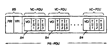
In Figure 24A a PR-PDU-cell comprising a number of VC-PDU:s is
shown. A PR-PDU-cell of this type may comprise two or more VC-
PDU:s. In Figure 24 three such VC-PDU:s are shown. Each VC-PDU 84
represents a VC-PDU-cell, i_e_ a micro cell of the VC-layer, that
has been put in a PR-PDU-cell 85 provided with a PRI- and a VPI
identifier which are common to all the VC-PDU-cells. The PR-PDU-
cell 85 is still referred to as a mlcro ceil. Each of the VC-PDU-
cells 84 in Figure 24 are bound for the destination indicated by
the PRI and VPI values. This destination is the last point along
the route which the VC-PDU-cells 84 have in common. In the
example given in Figure 4 this point correspond to access unit
AUl in access switch AS4 The individual VCI values of the VC-
PDU-cells 84 may differ from VC-PDU to VC-PDU within $he PR-PDU-
cell 85. The VCI identifiers shown in Figure 24A do not belong to
the header of-the VP-PDU-cell 85 but form part of the user data
thereof. This is an important feature of the present invention.
By stuffing several VC-PDU:s 84 into one PR-PDU-cell 85 the delay
in forwarding celIs from their origin to their destination is
red~ced. This can be clarified by the following metaphor: Suppose
the PR-PDU-cell 85 is a train bound for New York (corr~cp~n~ing
to the last point where the VC-PDU:s 84 are traveling in common).
The individual VC-PDU:s 84 are bound for different cities away
from New York. As soon the VC-PDU:s have filled the PR-PDU-cell
85 the PR-PDU-cell, that is the train to New York, is dispatched.
In New York the VC-PDU:s 84 leaves the New York train and takes
individual trains to their respective cities. Thus the waiting
time at the originating station will be reduced to the time it
takes to fill the New York train (the number of VC-PDU-cells 84
making up the New York train) which is short compared to the time
it would take to use separate trains 84, (PR-PDU-cells~ one for
each destination city. Such separate trains would have to be
completely filled with passengers (time slots) bound for the
particular city until the train would be allowed to leave its
originating station.
21 9~45~
W095/34977 34 r~ h~ 0
Figure 25 is ~icr.lncing the PR-PDU-cell 85 of ~igure 24A when it
is traveling at the VP-layer. In Figure 26A the ina~ividual VC-
PDU:s of the PR-PDU-cell 85 are shown=in the way they look like
when traveling in the VC-layer.
In the exemplary PR-PDU-cell 85 shown in Figure 24A only three
VC-PDU:s are shown although more such VC-PDU:s may be contained
therein as has been intimated by the dots.
In Figure 26A a PR-PDU-cell comprising a standard AT~-cell~of 53
bytes size is shown. The PR-PDU-cell is 56 bytes. The user data
of the ATM-cell has been filled with a number of VC-PDU-cells.
Figure 27 is a simplified block diagram of a switch provided with
means for supporting the specific features of the present
invention. The switch shown is any of the switches ASl-AS4
or CSl in Figure 4. A conventional cross bar ATM switch 86_has a
number of input lines 87-1.... 87-n and a number of output lines
88-1 .88-n. In the preferred embodiment of the invention the ATM
switch 86 of the type shown in my U.S. patent application
08/011378 filed on January 29, 1993, which is i~uL~ul~L~d by
reference herein. Each input line 87 is connected to a respective
access unit AU. To each input line there is connected a celL size
and routing means 89. Cell size and routing means 89-1 is
connected to input line 87-1 etc.~up to:cell size and routing
means 89-n which is connected to input line 87-n. By way of
example input line 87-1 is connected to AU3 while input line 87-n
is connected to AU4. At each of the output lines 88-1...... 88-n
there is connected a respective c~ll C17.~ ~r.n~ing means 90-1 ...
90-m. Since the cell size and routing means 89 are identical only
cell size and routing means 89-1 will be described. It comprises
2 multiplexor 91, control means 92, a PRI-conversion table 93 and
cell size counter 94. The multiplexor 91 has two input lines, one
being input line 81 fQr the cell stream and the other denoted 97
from PRI conversion table 93. The multiplexor 98 has an arm 98
movable between the two input lines 81, 97 and is ~ul,ne~L~d to
the input line 87-1 of the cross bar switch 86. The main function
of the cell size and routing means 89 is to establish which cell
size an incoming cell has, to route an ~n( ing cell according to
2 ~ ~ D4 59
w09~l34977 35 ..~
its PRI and to change the PRI value of an i n~ ~t ng cell to a new
PRI vaLue indIcatlng the source of the cell~ T~3 routing is done
in a conventional way using the PRI conversion table 93. From the
int ~ng cell stream 81 the fields containing the slze code, i.e.
the format indicator and the CTF-field, are decoded, by cell size
decoder 55, and loaded into the cell size counter 94. The cell
size counter and the control means 92 analyses the ~ n~ ~ ng cell
stream in order to keep track of each incoming cell and as soon
as a cell has been identified its PRI value is extracted. The
extracted PRI value is used to address the PRI conversion table
93. The PRI value of the incoming cell indicates the destination
of the cell or rather the PR trail sink. The value is switched to
a new PRI value, taken from the PRI conversion table, indicating
the source of the PR trail, in this case telephone unit T5. In
this way the termination sink, when analyzing the PRI value will
get information on w~ich the sender is. ~hen the cell header is
identified arm 98 moves to input lines 97 and the new PRI value,
i.e. the PRI value of the orlginating unit, is inserted into the
cell header and thereafter arm 98 moves back to input line 81 and
the cell will be passed on onto input line 87-1. Although not
described the cross bar switch 86 comprises input buffer and
buffers at each cross point of the cross bar as well as output
~ueue buffers.
At each of the output lines there are st~nn1nJ units, not shown,
which scans its respective output line to see if there is a cell,
at any of the input lines 87-1...87-n, which is bound for its
output line. If so, the corrt~spt nt~ ng scanning unit activates a
cell extraction unit, now shown but conventional, which then
extracts the cell. Since the cell size tlt~ootling means 90 are
identical only cell size means 90-1 will be described. The main
function of each cell size decoding means 90 is to keep track of
the various PR-PDU sizes in order to maintain the cell framing.
i.e. to know the cell size and to know how many octets that
should be transferred through the cross bar switch. The cell size
decoding means comprises a cell size decoder 95, similar to that
at the inputs, and a cell size counter 96.
21 9~45q
W095/34977 36 ~ 5'0l'/a
In Figure 28 the address s~ructure~useq in each of the units of
an ATM node 2 is sho~n This address structure is~accor~iingly
used in the access units, in the access switches~Al, in the
mapper units M and in the central switch CS. There is a physical
route table, PR-table, 140 having a number of entries 0-23. With
each entry there is associated a virtual path table 141. Each VP-
table has a number of entries 0-255_ TD each such VP-table entry
there is associated a respective virtual connection table VC-
table 142. Each VC-table has in turn a number of entries 0-255.
Each entry in the PR-table 140 corresponds to a physical route.
Since there are 24 entries in the PR table 140 there are 2g VP-
tables 141 To each=V~-table 141 tbere is associated 24 sets of
VC-tables 142 each such set comprising 256 VC-tables 142. The
PRI-identifier, i.e. the pointer in the entry of the PR-table
140 points out the VP-table to be used. The VPI identifier~ i.e.
the pointer at an entry in a VP table points out which of the 256
VC-tables that should be used. The VCI pointer in turn points out
the position in the used VC-table.~Accordingly there are 1 ~ 24
~ 256 ~ 256 addresses that can be addressed, i.e. 24 . 64k
addresses are available. Instead of grouping the addresses in
various tables in the manner shown in Figure 8 it is posel hl P to
use a long linear array containing 24 . 64k ~d~rP~eP~. Other
address structures are also possible.
Next the mapper units MU1-MU4 will be described with reference to
Figure 29. Since these units are identical only MU1 will be
described. Mapper unit MU1 comprises means 100 for h~ndl;ng cells
at the PR-level, means 101 for h~nflling cells at the VP level and
means 102 for handling cell as the VC-level. The means 102 for
h~n~ling cells at thq VC-level will provide for=putting VC-PDU:s
in PR-PDU-cells as well as for cell disassembly. The mapper unit
has also an input fifo lD3 and output fifo -104. A fifo is a
register of the type first in first out wherein the bits of each
octet of the cell are stored in se~uential order. Cell h~ndlin3
means 100 comprises a PR table 105 and a multiplexor 106 having
two input lines 107, 103, a movable arm 109 and an output line
110. The PR- table 105 comprises a:number of entries illustrated
by the horizontal lines. Each entry stores either a VP-pointer or
a new PRI-value. To each entry a ~ualifier~Ql is associated. The
21 93459
W095l34977 37 r~ ~ . I a
qualifier Q1 is~used to~identify the signLficance of the value
stored at its associated entry.-If for example Q1=1 the value
stored at the entry is a new PRI value. If Ql=0 value stored at
the associated entry is a VP-pointer which points to the VP-table
to be used for the particular entry.
Cell handling means lQl comprises a number of VP-tables 110, a
multiplexor 111 having an input line 112, an input line 113, a
movable arm 114 and an output line 115. Each VP-table 110
comprises a number of entries. At each entry there is stored
either a VC-pointer or a new VPI or the size of the cell. To each
entry there is associated a qualifier Q2. Q2 indicates whether
the information stored at its associated entry is a VC-pointer,
a new VPI value or a cell size. If for example Q2=0 then the
values stored at the corresponding entry are new PRI- and new
VPI-values. If Q2=1 then its associated entry stores a VC-
pointer, i.e. ~a point-er to the VC-table associated with the
particular VP-table entry Cell h~ndling means 102 comprises a
number of VC-tables 116, a multiplexor 1~ having two input lines
118, 119, a movable arm 120 and an output line 121. Each VC-table
comprlses a number of entries. To each entry there is associated
a qualifier Q3. The information stored at a particular entry in
the VC-table is either new VPI-. PRI- and VCI-values or an
instruction to put two or more VC-PDU-cells into a PR-PDU-cell or
an instruction to terminate the circuit at the mapper unit. The
significance of the information stored at the entry is detPrm~npd
by Q3. If for example Q3=00 then new VPI-, PRI- and VCI-values
are present if, Q3=01 then the information stored at the entry is
an instruction to put a number of VC-PDU-cells into a PR-PDU-cell
and if Q3=11 then the information stored at the entry is an
instruction to terminate the circuit at the mapper unit. Cell
hnn~ling means 102 also comprises a number of VCU-PDU fifos
121-1. .122-n,~where n represents the maximum number of VC-PDU:s
that can be put in a PR-PDU-cell. A multiplexor 123 has a movable
arm 124 which is connected to the output lines 121. The multiple-
xor 123 has a number of output lines, schematically shown at 125.
Each output line 125 is connected to a respective VC-PDU fifo
122. Cell h~n~l ing means 102 also comprises a multiplexor 126
having a number of input lines 127, a movable arm 128 and an
2 ~ ~04 5~
W095/~977 38 ~ O
output line 12~. Each input line 127 is associated with a
respective VC-PDU fifo 122
The mapper unit also comprises a main multiplexor 130 with four
inputs, a movable arm 131 and an output line 132. The inputs are
connected to the output lines 110, 129, 115 and 121 respectlvely
and the output line 132 is connected to the output fifo 104. The
mapper unit also comprises a cell size counter 133, a VC-PDU size
counter 134 which together operate in order ta distinguish the
cell header from the cell payload a~nd to distinguish various VC-
PDU:s of a PR-PDU-cell from the PR-PDU-cell header.- :
The operation of the mapper unit will next be described in
connection with the flow charts shown in Figures 30, 31 and 32.
Cells arrive at random at the input buffer 103 wher:ein they are
temporarily stored The PRI-value of the cell in the input buffer
103 is analyzed, block 140. Next the entry ~UL,~a~onding to this
PRI-value is entered in the PR-table 105, block 141. In Figure
129 this is indicated by arrow 137. Next the~ualifier at the
cited entry is analyzed, block 142. If Ql=0 then the cell should
be bridged by the mapper unit, i.e. the old PRI-value should be
removed and should be replaced with a new PRI value If Q=l then
no bridging should be made at the PR-layer and the cell should be
further processed. I~ Ql=0, alternative "yes" at the ~ inn
block 143, then arm 109 of multiplexor 106 moves to the indicated
position and the new PRI-value is fetched from the entry and is
transferred over output line 110 to the output fifo lû4 via the
main multiplexor 130 which has been brought into the indicated
position by the selector:control 135. This procedure~is indicated
in block 144. Next the PR-SDU of the cell in the input fifo 103
should be transferred from the input fifo via input line 108 and
output lines 110, 132 to the output fifo 104 wherein it is added
to the new PRI value stored therein. Compare box 145 The cell in
the output fifo 104 is ~ow~dispatched, box 146, and input fifo
103 is empty. As soon as a new cell arrived to the mapper unit it
will be stored in input fifo lC3. ~
If ~ualifier Ql=l, then the value stored at the corresponding
entry represents a pointer, in particular a VP-pointer pointing
2 ~ 9~59
/34977 39 r~ /a
out the particular VP-table, amongst-the VP-tables 110, that
should be used Thzs is indlcated by arrow 138 and is represented
by block 147 in Figure 30. Next the VPI is fetched from the cell
in the input fifo 103. This is indicated by arrow 139 in Figure
29 and is represented by bLock 148 ~in Figure 30. This VCI
indicates the entry to be used in the selected VC-table, block
149. Next, the qualifier Q2 has be investigated in order to find
out the significance of the information stored at the entry
specified by the VCI. Shall the cell in the input fifo be bridged
at the VP-layer or=shall it be further processed at higher layers
of the protocol? This decision is taken at the decision block 150
in Figure 31~ Similar procedures as described above will now take
place. If qualifier Q2=0 then bridging should take place, that is
the cell should be transferred from the input fifo 103 to the out
fifo 105, its old PRI and VPI values should be removed and be
replaced by new PRI- and VPI-values stored at the entry pointed
out by arrow 139. This is done by multiplexor lll. Its arm 114
takes the position shown in Figure 29, the new VPI value is
fetched from entry and is transferred via output lines 115. Main
multiplexor 130 is set to the input at which output line 115 is
connected and the new VPI-value is stored in the output fifo 104.
This is represented in block 151. Next the arm 114 is set to the
input line lI3 and the rest of the data, any VCI:s included,
stored in the input fifo 103 is transferred to the output fifo
104. This is represented in block 152. Arm 114 then return to the
position shown in Figure 29. As described above the m~ VG ts of
the arms 114 and I31 are controlled by the selector control L35.
At the entry pointed out by arrow 139 there is also information
available relating to the size of the cell to be outputted. The
size of the celL at the input fifo 103 is fetched by the cell
size counter which reads the PSC field of the cell at the input
fifo. When the slze fetched by the cell size counter 133 equals
the si~e value stored at the entry at the VP table no more octets
should be read from the input fifo 103 since the cell at the
output fifo is now complete. The selector control 135 is using
this fact in order to control the movement of the arm 114. Since
the cell at the output fifo now is complete it will be dis-
patched, block 153.
21 ~5~
WO95/34977 90 P~ l~D~ /a O
If the analysis o~ ~he Q2 at the entry poi~nted out by arrow 139
in the selected vP table reveals that Q2=1, the value stored at
this entry signifies a pointer, in particular a- VC-pointer
pointing out the VC table, amongst the VC tables 116, to be used
for the particular cell in the input fifo 103 This is represent-
ed by arrow 160 in Figure~ 29 and by block l54 in Figure 31. Next
the VCI of the cell in the input fifo should be fetched. This is
represented by block 155. This VCI-=value is also the number of
the entry to be used in the selected VC t~able,This is represent-
ed by arrow 161 in Figure 29 and block 156 in Figure 31. Once the
entry has been selected the qualifier Q3 associated with the
entry is ~U~m~ n~, block 157. ~ =
The Q3 qualifier can start one of three processes accor~ing towhich the VP-PDU user data conte~ts pf the cell in the input fi~o
103 should be handled, The processes are eithe~ VC-PDU bridging
from one VP trail to another, VC-PDU termination or~filling VC-
PDU into a PR-PDU-cell. VC-PDU bridging takes place if Q3=00.
This process corresponds to the VC-PDU dotted line indicated in
the protocol stack of Figure 9. If Q3 inaicates that bridging
should be made, then the corresponding entry contains new VPI-,
PRI- and PCI- values to be attached to the VC-PDU of~the cell in
the input fifo_ The new values are fetched from the entry pointed
out by arrow 161 in the selected VC-table and appear at input
line 118 to the multiplexor 117 the arm 120 of which has been
brought into the shown position by the selector control 135.
These new values are transferred from the output line 121 to the
corresponding input of the main multiplexor 130 the arm 131 of
which has been set to the position corresponding to the input
line 171 by the selector cPntrol 135. The new VPI-, PRI- and VCI-
values are stored in the output fifo 104 ~his is indicated inblock 159 in Figure 32. Next arm 120 is moved to the position
corresponding to line 119 and the rest of the data of the cell in
the input fifo 103 is transferred v~a input line 119, input line
121, arm 131 and output line 132 into output fifo 104. Arm 120
then returns to the position shPwn in Figure 29. This is
indicated by block 160 in Figure 32. The PR-PDU-cell in output
fifo 104 is now complete and is dispatched, block 161.
2 ~ 9~4~9
Wo~5l34977 41 P~ 5,'C ,/~
If several VC-PDU:s are to be put into the VP-PDU part of a PR-
PDU-cell of the type shown in Figure 25 this will be lndlcated by
the quallfier ~3. No bridging should be made in this case,
instead the PRI- and VPI- values of the PR-PDU-cell stored in the
input fifo 103 should be analyzed, block 162 Each VC-PDU fifo
122-1...122-n is associated with an outgoing VP-trail. Based on
the analysis of the VPI value the corresponding VC-PDU fifo 122
is selected by the selector control 135 which moves arm 124 of
multiplexor 123 to the selected VC-PDU fifo. Each VC-PDU fifo has
pre-stored therein a new PRI-value and a new VPI-value in order
to be able to dispatch a complete cell when it is filled with VC-
PDU:s When the VC-PDU has been stored in its corresponding fifo
122 it resides there and waits for another VC-PDU bound for the
same destination as indicated by said new PRI- and VPI-values.
The input fifo 103 is empty and is ready for receiving a new
incoming cell~ This is indicated in block 164. The processes
described above in connection with Figure 30, 31 and 32 are
repeated. The status of each of the VC-PDU fifos is supervised
and as soon as a ~ifo is full the PR-pDu-celL is dispatched. This
is achieved by moving arm 128 of multiplexor 126 to the input
line 127 associated with the filled VC-PDU fifo 122. The PR-PDU-
cell is dispatched over output line 129 to the main multiplexor
130 the arm of which has been moved, by the selector control 135,
to the corresponding input line 129 The PR-PDU-cell is immedi-
ately dispatched without further delay in the output fifo 104.
Since the PR-PDU-cell is comparatively long it will take some
time to dlspatch it completely and durlng thls tlme the cell
h~n~l ;ng means 100, 101 and io2 are idle. Meanwhile new cells are
stored in the input buffer 103. The VC-PDU fifo supervision
means, not shown in the drawing, also supervises the time during
which a VC-PDU is stored in each of VC-PDU fifos 122. If this
time exceeds a predetermined time, referred to as a time-out
llmit, the VC-PDU:s stored in a fifo are dispatched. The
remaining part of the VP-SDU will be filled with a dummy VC-PDU.
A dummy VC-PDU is lndicated by setting the VCI-127. Accordingly,
the time delay in dispatchlng the VC-PDU:s is controlled. No VC-
PDU:s will be "forgotten", l.e. wlll not remain undispatched in
the mapper unit. Referring to the example given in Figure 4 and
with reference to Figure 10 PR-PDU-cells 28'/1 and 29'/1 of
21 qO45q
W095l34977 42 .~ ''C
Figure 11 are~shown in Figure 29 to the left and the PR-PDU-cell
30-/1 is shown to the right in Figure 29. PR-PDU-cell 29'/1 is
the first one to arrive to_the iaput fifo 103. Its PRI points to
entry number 3 of the PR-table and the ~ualifier Ql points to a
VP-table and the VPI-value of.the cell points to entry number 2
in the selected VP-table. Ql~nli~;~r Q2 at this entry indicates
that VC-PDU:s should be put in a PR-PDU-cell and time slot TS#6
and its VCI-value is ~stored as .VC-PDU in the VC-PDU fifo
corresponding to the VP trail associnted with VPI#2. In this fifo
there ls pre-stored a~PPI=value of 1 and VPI-value of 2. The
input fifo 103 is now empty and recelves ,the next cell, cell
29'/1, which is analyzed in a similar way. Its time slot TS#6
together with a VCI value o~ 2 is stored i~ the,same fifo as the
previously described TS#5. The VC-PDU size counter has now
counted two VC-PDU:s and the VC-PDU fifo is now ready to dis~atch
it contents as a new larger PR-PDU-cell comprising in its header
PRI#1, VPI#2 and in its payload two VC-PDU:s 84. The VC-PDU
filling process that takes place in MU1 is indicated by line 31
in the protocol stack of Figure 9
Having described how the VC-PDU of-two cells are put in the VP-
PDU of another cell in mapper un$t MU1 the way this cell is
handled by mapper unit MU4 will next be described in connection
with Figure 33. The concatenated cell 30'J1 is i ~lily stored
in the input fifo 103_ Qllnlif;or Ql at the second entry of the
PR-table 105 indicates that a VP-table should be selected and the
qualifier Q2 at the second entry of the selected VP-table
indicates that VP-bridging should take place. PRI- and VPI-values
are fetched irom this entry and are stored in the output fifo
104. The old PRI- and VPI-values are discarded. The rest of the
cell in the input fifo 103 is transferred via the multiplexor 115
to the output fifo lQ~ from which t,he cell 130'/1 is dispatched.
The VC-parts of the cell comprising the VC-PDU:s are never
active.
In Figure 34_the receiving por~ion of an access urit is shown.
Since the receiving unit is identical for all access units only
that of access unit AU1 connected to ,AS4 in Figure 4 will be
described in detail_ln the re~oiving access unit cell disassem-
~ 994~
WO95134977 43 - ~
bly takes place. The cell disassembly will be described ln
general as well as in particular with regard to the PR-PDU-cell
30'''. In Figure 34 the receiving portion of the access unit
comprises a physical route PR-table lQ5, a number of VP-tables
110, a number of VC-tables 116, a time slot store 175, a time
slot counter 176 and a cell size counter 133, a VC-PDU size
counter 134 and a control unit 136. Elements which are similar to
those described in connection with Figure 29 have the same
referenoe numerals although physically they are different since
they are sitting in different units In the receiving portion of
the access unit the time relationship between the individual time
slots which have traversed the ATM node 2 should be restored,
i.e. the position of the individual time slots in the frame
should be restored. To this end there is a~time slot memory 175
and a time slot counter 176. The time slot counter receives a
frame sync signal from a local ciock, not shown, of the access
unit. This clock need not be synchroni~ed with the clock of the
STM nodes 3 Each VC-table 116 has a number of entries. This
number eguals the number of time slots of a frame. The time slot
store 175 comprises a number of locations, said number also
corresponding to the number of time slots in the frames of the
time slot stream leaving the access unit AU1. In this case the
outgoing time slot stream is carried by a local line to which the
telephone units T1-Tn are connected.
The operation of the receiving portion will be described next
with regard to Figures 34 and 35. T 1 nS PR-PDU-cells are
stored in the input fifo 103. Next the PRI-value of the PR-PDU-
cell in the input fifo is fetched, block 190. The PRI-value
indicates the entry in the PR-table 105 that should be used
together with this particular cell. This is indicated in block
191. This entry contains a pointer to the VP-table that should be
selected amongst the VP-tables 110. This selection is represented
by arrow 138 in Figure 34 and by block 192 in Figure 35. Next,
the VCI-value of the PR-PDU-cell in the input fifo 103 is
fetched. The VCI-value indicates the entry to be used in the
selected VP-table. This is represented by arrow 137 in Figure 34
and by block 193 in Figure 35. As described above each entry is
associated with a qualifier. In this particular case the
2 1 904 5q
W095~4977 44 r ll~h -'C~S/a
qualifier, labeled Q4, indicates whether the cell is a single
micro cell or a cell c~n~aining a number of VC-PDU:s. If it is a
single micro cell then Q4 indicates that the value stored at the
selected entry is a write address indicating at which position
the time slot of the in~ ing PR-PDU-cell should be stored in the
time slot store 175. This is indicated at block 195 in Figure 35.
Since the PR-PDU-cell in the input fifo 103 may contain several
time slots, i.e. the cell may be of any of the types shown in
Figure 6 and 7, then the VP-table con~ains several additional
write addresses: each such additional address indicating the
address at which the associated time~slot should be stored in the
time slot store 175 Accordingly, an analysis is made whether
there are additional write addresses at the entry in the selected
VP-table. This analysis is represented by decision block 196.
Each such additional address is stored in the time slot store
175. This process is repeated until there are no more time slots
left in the input fifo 103. Finally the time slots stored in the
time slot store 175 ~Xe read by means of the time slot counter
176. The time slot counter starts at 0 for every 125 us frame of
the outgoing STM time slot stream. The counter 176 counts up to
the number of time slots contained ;n the frame and this is done
cyclically for every frame. At every count of the time slot
counter 176 data contained in the time slot at the corresponding
location in the time slot store is fetched. For example, if the
frame contains 24 time slots then location 1 in the time slot
store corresponds to time slot number 1 in the frame, location 2
corresponds to time slot number 2 in the frame etc. up to
location number 24 in the time slot store which corresponds to
time slots 24 in the frame. Time slot 1 in the frame may be
assigned to telephone unit 1, time slot 2 to telephone unit 2
etc. The read out the time slots stored in the time slot store
175 is indicated in block 197 in Figure 35.
If o,ualifier Q4=1 the significance of the value stored at the
entry of the selected VP table is a pointer that points to the
VC- table 116 to be used with the particular micro~cell in the
input fifo 103 Accordingly a VC-table is selected. This is
indicated by arrow 170 in Figure 3~ and block 198 in Figure 35.
The selected VC-table contains as many write addresses as~there
2 1 ~34~q
wogs/34977 45 r~ r ~S/a
are time slots in the PR-PDU-cell in the input fifo 103 Next the
VCI-value of the PR-PDU-cell in the input fifo is fetched This
is represented by arrow 177 in Figure 34 and block 199 in Figure
35. The fetched UCI-value points out the entry to be used in the
selected VC table. This in indicated in block 200. At this entry
there is stored a pointer, i=n particular a pointer to the
location in the time slot store 175 at which the time slot of the
cell in the input fifo 103 should be ~stored Accordingly the
pointer in the VC table is a write address that points out the
position in the time slot store at which the time slot should be
stored This write address and the position it points to has been
indicated with arrow 178 in Figure 34. The transfer of the time
slot of the ceIl in the input fifo to this write address is
indicated by arrow 179 in Figure 34. In block 201 of Figure 35
the last two procedures are indicated
If the celL comprising the VC-PDU:s at the input fifo 103
comprises more than one VC-PDU then the process described in the
paragraph above is repeated until all VC-PDU:s have been handled.
The time slot counter 176 runs continuously and the time slot
memory will be emptied each 125 usec.
The PR-table in Figure 34 differs from- the PR-table described
previously in that there is not any ~ualifier associated with an
entry. This is so because all PR-PDU-cells arriving to the
receiving portion of an access unit will be termlnated at the
access unit.
Applying the aboYe procedure on the cell 30''' shown in the upper
left of Figure 34 a PRI-value of 2 indicates that the second
entry of the PR table 105 is associated with the cell 30'''. At
this second entry a certain VP-table associated with this cell
should be pointed out. Next the VPI-value is fetched and this
value is 2 which means that the second entry of the selected VP-
table should be addressed. At this second entry the qualifier is
analyzed and in this particular case it is found that Q4=l which
means that the cell at the input fifo 103 contains VC-PDU:s
Therefore the value stored at the entry of VP-table signifies a
particular VC table. This VC-table is selected and the first VCI
2 l ~ q
WO95l34977 46 P~ 'la
of the cell is fetched at the input fifo 103_ This VCI equals 3
and therefore the third entry of;the selected VC- table is
addressed. The value stored at this third entry iS 4. ~r.rnr~l ng-
ly, the location to be selected in the time slot counter is
location number 4 at which the time slot TS#6 is stored. The VC-
table is analyzed once again and i=t is found~that:there ~is a
second VCI in the cell at the input fifo; this second VCI being
equal to Z. Accordingly the second entry in the selected VC-table
is addressed. At this second entry there is stored the write
address "8" Accordingly location number 8 in the time slot store
should be addressed and TS#5 is transferred via the line
indicated by arrow 179 to the 8th position. This is indicated by
arrow 178. No more VCI:s are found in the selected VC-table and
accordingly the input fifo is empty. When the time slot counter
starts a new frame and steps from location to location in the
time slot memory, it will pick up time slot TS#5 at location
number 4 and will put this TS#5 into time slot number 4 in the
outgoing cellstream. Next, time slot counter arrives to location
number 5, finds nothing, steps to location 6, finds nothing etc.
and finally at location 8 it will find time slot TS#6 which it
will take out and put into time slot number 8 in the outgoing
time slot stream. In this way telephone set T4 will have a
connection with telephone set T5 in AU3 and trlrrhnn~ unit T8
will have a connection with telephone unit T6 in AU4.