Note: Descriptions are shown in the official language in which they were submitted.
W0 95133198 2: q 0 6 4 3 P~ ,5,'~[ ~8
Process for detecting evanescently excited lu~ su~
The present invention relates to a process for detecting evanescently excited lu."i"esc~:"~.
with a planar dielectnc optical sensor platfoml based on a waveguide. The invention also
relates to the use of said process in qualitative affinity sensing and to the use thereof for the
selective quantitative d~ llillai;ul~ of lu~ sctn~l ,ù,~.u,,~ in optically turbid solutions.
The invention further relates to a sensor platform suitable for carrying out the process
Where light ~,U,uaydl~:, in a waveguide, the lightwave is not completely limited to the actual
waveguide: in fact a fraction of the lightwave ~,, Upayd~ in the contiguous optically thinner
medium. This fraction is temmed the evanescent field and is the basis of the variegated use
of optical waveguides in sensing technology.
With the cv~ l field it is possible in particular to excite lu, ,,i,l~:,cc~ in the optically
thinner medium. This excitation is limited to the immediate ~ i.ul ""~"l of the interface of
the waveguide. Evanescent IU"I;I ~ excitation is therefore of great interest foranalytical purposes.
A planar sensor consists in the simplest case of a 3-layer system: a substrate, a wave-
conducting layer, and a c, ~rerstrAtP that usually constitutes the sample for assaying.
Especially in the case of thin waveguides in which the thickness of the waveguiding layer is
smaller than the light wave length, the number of diflusible modes of the light field capable
of ,u~upaydliul~ is limited to a few discrete waveguide mor~es.
In the case of thick waveguides, a host of modes can be guided. In this case the need for a
substrate can often be dispensed with, for example for ll li-,k~ less~s in the range of several
1/10 mm and greater.
Prior art methods of detecting evanescently excited luminescence can be di~ lidL~:d in
accordance with the choice of radiation fractions that can be detected:
WogSr33l98 2 ~ 90643 r~l,~. o~ ~
.
- 2 -
Detection of the "volume lu~ sc~ ". a fraction of the fluorescence excited by the
guided wave is emitted into the full space angle; this fraction can be optically recorded and
fed into a detection system.
lJ
Detection of the "evanescent lu~ llvCI". cu,~,ul~",a"~dry to the lu",i"es.;~"~;~emitted into the space, this evanescent Il""i"~ "ce Is back-coupled as guided wave into
the waveguide, l, dl l:~,lJUI I~d there and coupled out via ~he end plane of the waveguide.
Methods and apparatus for detecting the evanescently excited lu, "il1as~ of antibodies
or antigens labelled with luminescent dyes are known and described inter alia in US-A-
4582809. The a"d~ claimed therein uses an optical fibre and endface coupling forthe evanescent lu",i"~s~"c~ excitation. Such optical fibres typically have a diameter of up
to 1 millimeter and conduct a host of modes when laser light is coupled thereinto. The
evanescently excited lull,i"~sc~"c~ can be measured in simple manner only by the fraction
tunnelled back into the fibre. The quite large di",e,~siu"~ of the apparatus and the fact that
,d;;~ly large sampling volumes are required are further drawbacks. The apparatuscannot be substantially reduced in size or even miniaturised to integrated optical sensors.
An ~"lla~ I of the sensitivity is usually associated with an increase in the size of the
apparatus.
A further drawback is the sensitivity wl1ich is limited by the endface output-coupling: as
excitation and l~",i"esct:, lc~ radiation run co-linearly and have to be separated by beam
splitters and filters (e.g. cut-off filters or band-pass filters), the di~;lilllilldIiùl~ ~:lldld~ Ik;~
of the filter unit limits the detection sensitivity.
The use of thick planar multimode waveguides is described by D. Christensen, D. Deyer, D.
Fowers, J. Herron in "Analysis of Excitation and Collection Geometries for Planar
Waveguide Immu,1ust" ,s~, .", SPIE 1~86 2(1993) (Fibre Optic Sensors in Medical
Diagnostics). Here the excitation radiation is coupled into the waveguide via the endface
and the lu",i,1t,~ "ce light emitted into the space angle is detected. Altematively it is also
possible to use an endface output-coupling. In this latter case, the limitation of sensitivity
caused by the necessary beam splitters and filters are a drawback in the same way as in
WO 95/33198 2 1 9 0 6 4 3 P ~ . V
the a"dnu~",~"~ described above. Further disadYantages here are also the large sensor
aiOI~:~ and the large sample volumes associated therewith.
In WO 90/06503 there is disclosed a process for exciting k""i,~sc~:n~ by total intemal
reflection fluorescence (TIRF) using thin planar, preferably monomode, waveguides. The
waveguide in this process is used to increase the light field strength at the sensor surface,
the excitation radiation being beamed in from the underside and reflected totally at the
sensor. The volume lu",i,1e~c~ emitted into the space angle is detected. In this process,
the interaction zone between excitation light and molecules having luminescent properties is
limited on the sensor, as excitation takes place only in the area of the beam diameter.
There are therefore only limiter,l F ' "" of li" ,~":,iu"i"g the sensor via the beam
diameter, with restrictions in diameter and divergence owing to the very narrowly confined
resonance angle.
The prior art use of one or more than one coupling grating for the input- or output-coupling
of guided waves is described by K. Tiefenthaler and W. Lukosz in "Sensitivity of grating
couplers as integrated-optical chemical sensors", J. Opt. Am. B6, 209 (1989), by W.
Lukosz, Ph.M. Nellen, Ch. Stamm and P. Weiss, in "Output Grating Couplers on Planar
Waveguides as Integrated Opitcl Chemical Sensors", Sensors and Actuators B1, 585(1gg0), and by T. Tamir and S.T. Peng, in ''Analysis and Design of Grating Couplers", Appl.
Phys. 14, 235-254 (1977). The processes described by Tiefenthaler et al. are useful for
affinity sensing by the direct detection method (via the change in refractive index). The
di~plact:n,~"~ of the coupling angle resonance is dt l~lll lil~d which, owing to the change in
refractive index, is governed by adsorption or binding of molecules.
Various attempts have been made to enhance the sensitivity of eva~ ";'y excited
h~l l lil ,~s~dn1e and to fabricate integrated optical sensors. ~hus, for example, Biosensors &
Gio~le~l,u"i~ 6 (1 g91), 595-6û7 reports on planar ,,,~(,v,,,od~ or low-mode waveguides
which are fabricated in a two-step ion exchange process and in which the coupling of light
into the excitation wave is effected with prisms. The affinity system used is human
immunoglobulinGflluorescein-labelled proteinA, wherein the antibody is illllll ' " ' on the
waveguide and the fluorescein-labelled proteinA to be detected, in phosphate buffer, is
added to a film of polyvinyl alcohol with which the measuring region of the waveguide is
, . , .. .. . .... . . ..... .... . .. .. ... ., .. . ..... . . . , _ _ _ _ .
wO 95/33198 ~3 1 9 ~ ~ ~ 3
- 4 -
coated. A substantial disadvantage of this process is that only minor differences in the
refraction indices between waveguidir~g layer and substrate layer are achievable, resulting
in a relatively low sensitivity.
The sensitivity is said to be 20 nm in fluorescein isothiocyanate bonded to proteinA. This is ,
still ul l~dLl~a.:lury for being able to detect ~ ulld~t:5, and a further t,~ al~ce" ,~"l of
sensitivity is necessary. Moreover, the reproducibility and practical viability of coupling light
into the excitation wave by prisms seems difficult on account of the c~ d~ldbl~
d~,ue,~.lence of the coupling efficienc~ on the quality and size of the contact area between
prism and waveguide.
The use of gratings for the lull ,in~s~ d detection as claimed in this invention is described
in US-A-5 081 012. This US patent discloses grating structures for coupling excitation light
into a waveguide as well as special reflection gratings which enable the excitation wave to
traverse the waveguide a number of times. Enhanced sensitivity is said to be achieved by
this means. The volume lu",i,~s.,t:l ~ce emitted into the space angle. Moreover, the
excitation radiation coupled out of the input-coupling grating after two traversals can be
used as reference signal. The drawback of this process is the strong increase of the
background radiation intensity caused by the reflection grating and which is emitted with the
lu~ li"es~ ce signal into the space angle. The ~l lal d~ s of the necessary filters once
again limit the detection sensitivity.
The invention has for its object to provide a process for d~" "il lil l~ lu" ~ "~ with a
planar optical waveguide, which process is simple and ecu"u",i~.A'ly viable and for which, in
particular, only small sample volumes are necessary. It is a further object of the invention to
provide a miniaturisable sensor platfomm on the basis of a planar optical waveguide for
carrying out the process.
This object is achieved with a process for ~ li"9 lul"i"ds~"~ with a planar dielectric
optical sensor platfomm which consists of a lldl~,ual~ substrate (a) to which a thin
lldlls~al ~l ll waveguiding layer (b) is applied, which sensor platform is provided with a
coupling grating for the input coupling of the excitation light and the refractive index of said
substrate (a) is lower than the refractive index of the waveguiding layer (b), by bringing a
liquid sample as superstrate into contact with the layer (b), and measurfng the lu",il,~s~el,ce
,, _ , . .. = .. .. ....... . .. _ . _ -
W0 95133198 2 1 9 0 6 4 3
.
produced by substances having lu",i"e:,c~ e properties in the sample, or by substances
having l~ ld~C~IlC~ properties i""~ on the layer (b), o~ .eld-;l,u"ic~:!y, by coupling
the excitation light with the coul~ling grating into the planar waveguide so that it traverses
the waveguiding layer, whereb~/ the substances having lu",i"esct~"~e properties are exclted
to lu",i"dsc~:(,ce in the evanescent field of the waveguiding layer, which process comprises
using a waveguiding layer having a thickness smaller than the wavelength A of the
excitation radiation and which consists of a material whose refractive index at the
wavelength of the excitation radiation is 21.8, and coupling out from the waveguiding layer,
and detecting, the lull,i,1~:~c~ radiation coupled back into the waveguiding layer (b) with
a second coupling grating spati~lly separated from the first coupling grating.
Preferred utilities of the process form the subject matter of claims 20 to 23. A sensor
platform and the preferned ~Illbo.lilll~ thereof which are particularly suitable for carrying
out the process of the invention are described in claims 2~1 to 38. Preferred e",bDdi",e"l~ of
the process fomm the subject matter of claims 2 to 19.
In the practice of this invention, the excitation radiation is coupled into the waveguide with a
coupling grating and p,u~Jay..'~c in the waveguiding layer as guided wave. For the efficient
eva~ "l excitation of the l~"~ id it is possible to achieve a high field strength at or
near the sensor surface by choice of the wavelength pdldlll~ (refractive index, layer
thickness).
Surprisingly, it has been found that, for the ~ iu"i"~ of the waveguide described
hereinbelow, a substantial fraction of the lu",i,1~s~d"ce radiation is coupled back
evanescently into the waveguide and is l,d"~.o,l~d by the waveguide together with the
excitation wave. Hence the lu",il1ds~nc~ radiation can be coupled out of the waveguide via
a second coupling grating which is spatially separated from the first coupling grating and is
conducted to the detection system. The advantage of this ''grating detection evanescent
luminescence" over the ''volume detection" of the prior art resides in the simplified possibility
of minitiaturising the sensor plat~orm and the detection system pertaining thereto.
The dimensioning of planar waveguides for the most efficient luminescence excitation
possible can be effected on the basis of the theory of planar waveguides. The following
_ _ _ . . .. . .. . .
WO95/33198 ~ ~ q~ 3 rc~
.
- 6 -
di",el~iv":, are in this connection to be observed (W. Lukosz "Principles and sensitivities of
integrated optical and surface plasmon sensons for direct affinity sensing and
imm~" lu5~ Iy'', Biosensors & Biu~le,,l,u"i~ 6, 215-255 (1991), il.G. Hall, "Optical
waveguide diffraction gratings: coupling between guided modes", in Progress in Optics
XXIX, ed. E. Wolf, Elsevier, New York (1991):
The penetratlon depth of the evanescent field of a planar waveguide into the superstrdte is
expressed by the equation
"' /" ~IN2~-n2
fûr the effective modal refractive index Ne~ the s~lre~tr~tQ refractive index nwp,,,, and for
the working wavelength ?.. In the above equation z denotes the c~"di"~t~ vertical to the
waveguide surface, x denotes the coordinates of the waveguide u,~ ic . Taking into
accountthe~ld,,~d,~i~dliu,~factorffortheelectricfieldstrengthatthewaveguidesurface
n fi,~, - N ~
~7 ~ 72 b
in which n",m is the refractive index of tlle waveguide and n",b is the refractive index of the
substrate, there Is obtained an intensity curve IE of the evanescent field above the
waveguide p,upù,liollal to:
iE~J-e ~.
This intensity curve of the exciting evanescent fields vertical to the waveguide surface
determines the essential scaling factor for dimensioning the layer thickness and refnactive
index of the waveguide. For analytical utilities for the detection of luminescent molecules in
the proximity of the waveguide layer, it is necessary to take into account the distance of the
molecul ~ from the waveguide surface when ~i,,)~,)siul ,i"g the waveguide.
W095133198 2l 90643 r~l,~,s,. ,~
.
-- 7 -
For luminescence detection it has now been found that the evanescent back coupling of
Iu~ ds~,~"~,~ is an efficient process for thin, highly refractive planar waveguides.The
choice of layerthickness and refractive index has an effect on both the (computable)
excitation efficiency as well as on the c~ a~tn 11 back coupling. In the latter case there is
cu,,,~: " , between the input-coupling of the radiation fractions of bound molecules in the
proximity of the waveguide surfilce and the input-coupling of unbound molecules from the
sample volume.
For an efficient detection of molecules having luminescenl properties in the proximity of the
waveguide surface by the process of this invention it has been found that the waveguide
pald"~ , must lie in the follo~Ang range:
. refractive index n~i~m ~1.8 for the excitation wavelength ~,
, layer thickness t~ilm S for the excitation wavelength ~, preferably t~j~m S ~IJ2.
Aparticularlyadvantageous~:",l,u~i",d,lloftheprocessisthatwhenthelayerthicknessis
selected in the range from 40 to 1 60nm, and simultaneously the depth modulation of the
gratings is from 3 to 60nm, the natio of depth modulation to layer thickness being ~0.5.
These wavelengths can also be ~ ald~ d~ in that they typically pemmit only the
~)1 U,Ud~dli~l I of waveguide modes of low order m S ~.
The lul"i,lt:sc~"ce which is evd~ "lly coupled back into the waveguide is lldll:,,uo,lted
therein; ~llala~ therefore is the attenuation coefficient r of the guided wave. Given a
low Stokes' shift, identical atten~lation data for the excitation and lulllil~ llcd radiation
can be assumed (possible causes of the waveguide decay ane scattering losses at the
interfaces of the waveguide as ~lell as absorption in the waveguide layer or in the substrate
or cllrerstrAt~f~ If there are no pronounced narrow absorption bands, then no significant
change in decay caused by the Stokes' shift of typically 10-50nm is to be expected both for
scattering as well as for absorption. Such spectrally narrow-band absorption effects must be
avoided in selecting the material for the sensor platfomm).
wo95/33198 21 ~ 3 r~
- 8 -
This l~",i"~c~ e radiation lld~ ul~td in the waveguide must be coupled out and guided
to the detection system. An end-plan~ output-coupling is not expedient: on the one hand it
requires a high quality of the wavelength edges and in some cases contacting the optical
detection means via a liquid or gel irrmersion and on the other hand the integration of the
sensor elements together with the fluid cell is thereby hindered.
The use of a second coupling grating, which is spatially separated from the coupling grating
for the input-coupling of the excitatiorl radiation for coupling out the lul "i,le~ "~ radiation
is able to avoid completely the end-plane problem. A further advantage is that the grating
distance A in direction x (i.e. in the direction of the guided wave) can be freely chosen. The
possibility is thereby afforded of an optimum adjustment of the distance A to the attenuation
for each wavelength without the necessity of altering the external iil"~"~iu"~ of sensor and
fluid cell. Furthemmore, it is advantageous that the outside edges of the sensor element do
not have to meet any optical quality requirements, so that their configuration can be
adjusted to the fiuid ceil - in particulal to the uu~ of the sealing employed.
An optimum vaiue for the grating distance B has been found to be B = x1,e with a variation
possibiiity in the range of B - (û.2 - 3~ x1/e (X~b: 1/e iength for the drop in intensity of the
guided excitation wave in direction x).
(Conversion . r [dB/cm] ~ x", [1/mm]: x,~e=1ûû/(ln1û~r)).
Fûr greater distances, both excitation light as well as guided lul "i"es~i~n~ light is strongly
attenuated and iead to a strong signal reduction. The downward iimitation is not expressed
primariiy by excitation and back-coupling, but rather by the demands associated therewith
made of the positioning of both gratings and of the excitation radiation on the input-coupling
grating. Here spacings of iess than 1ûOjlm are i"expedi~"l also in view of the ii",~"sio,~i,)g
of the width of the input-coupling grating described below and the light diameter of the
excitation radiation on the edge of the input-coupling grating.
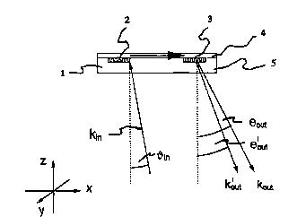
The invention is described h~ L . 'o~. in more detail by means of the figures.
Figure 1 shows a schematic sideview of an optical sensor platfomm which is particularly
suitable for carrying out the inventive process with a possible radiation curve.
wo 9~/33198 2 1 9 0 6 4 3 r~
g
Figure 2 shows a top view of the sensor platform of figure 1.
In Fig. 1, 1 is the sensor platforrn, 2 is the coupling grating for coupling in the excitation
radiation, and 3 is that for coupling out the l~ il ,r,s~ , 4 is the waveguiding layer and 5
is the substrate.
Fig. 1 shows a possible path of Irays for the input- and output-coupling of excitation and
lu",i,~sc~,~ce radiation into and out of the sensor plaffomm. A guided wave with u", ~
in direction x is excited by the coupling grating 2 in the sensor plane when the resonance
condition in respect of the x ~ul~ ,,uu, ,~"~ of the wave vectors is met:
kw~ = k,m + m*kG = k~a + nt*2~. . m: integer, kr,; reciprocal grating vector
kV,L = 27~ * N,ff = ko * N,~: wave vector-guided wave with effective modal refractive index
Nel~
In Fig. 1, a negative angle ~ is shown for the input-coupling with
kin=ko~cos~ (ko: magnitude of wave vector in the plane of the drawing)
so that the guided wave nuns in the "opposite direction" to the excitation (so-called
"backward coupling"). Positive alngles are chosen for coupling out the excitation wave (with
kou~) and the the l~""in~bce~ radiation (with kout)
A high degree of background fneedom ~s achieved by such an input- and output-coupling
cu, ' ~ IrRtinn with markedly different directions for neflected incident light and light which is
coupled out. The spatial separat~on of the different radiation fractions ensures an optimum
signal-to-noise ratio in l~lllil ,e~ u detection: excitation radiation which is coupled out and
lulllil~sct:~u~ radiation do not n~n in a common path of rays, so that fiiters (cut-off or
bal l~d,Ud~ filters, not shown in Fig. 1 ) are used only for suppressing scattered light, but not
for the full intensity of the excitation radiation which is coupled out.
A further advantage of using an output-coupling grating is that different spectral
~u~,,uun~ of the l~""il~s~e,l~ radiation are coupled out in different directions. It is
wo95/33198 2 ~ 9 ~ ~ 3 ~ a~t ~~
-10-
therefore possible by means of this invention to detect also molecules in weaklyluminescent sample media even without additional filters if the lu~ s~, ,c~ of molecules
to be detected and of the sample medium is spectrally different.
The adjustment of the angles for input- and output-coupling is possible through the choice
of grating constants A1 and A2. For the preferred case shown in Fig. 1 with a direction
separation between input- and output-coupling, the grating constants must be chosen with
marked differences.
Altematively, identical grating constants can be used for the gratings 2 and 3 to simplify
fabrication of the sensor. This may be important for as cost-effective a fabrication of the
sensor as possible, as a number of process steps are omitted when using I~JIUYI dpl~i~
structuring for grating fabrication. The spatial separation of the direction of excitation which
is coupled out and llrlllil ,es~n~ radiation is still ensured when using identical grating
constants. Only the safe separation of the direction of the reflected input-coupled radiation
is omitted, so that additional measures for reflection screening are necessary, e.g. using
apertures or light tnaps.
The coupling angles can be placed advantageously by the choice of the grating constants
in the range from ¦ ~ ¦ ~1 bis 50 (for tlle magnitude of the angle). Smaller values should be
avoided on account of the Bragg reflection, as othenwise this reflection occurs even at low
tolerances of the adjustment or of the levelness of the sensor, in conjunction with the non-
occurrence of input- or output-couplin~. Larger angles up to almost 9û are possible; but
angles far beyond the nommal ones for sensors should be avoided for a proper
implementation of the path of rays.
The ~ , laiul lil l9 of the grating depth can be in acGul ddl ,ce with the prior art (T. Tamir/ S.T
Peng "Analysis and Design of Grating Couplers", Appl. Phys. 14, 235-254 (1979); T. Tamir,
''Beam and waveguide couplers" in "Integndted Optics", ed. T. Tamir, Springer, Berlin
(1979). The so-called "leak parameter" r~ is used here as feature: rx describes the ~le
decrease in intensity of a guided wave in a waveguide whose interface is provided with a
coupling grating of depth t9,a,in9. Hence 1/rI is the r;l ~A~ length for ~rd~ "i"y the
radiation energy from the guided wave to a wave that p,upaydl~ freely or vice versa.
WO 95133198 2 1 9 0 6 4 3 P~
Important for the choice of the depth of the input-coupling grating is not primarily the
absolute value of the leak parameter, but the adjustment of leak parameter and the
radiation parameter of the incident light (beam diameter and divergence). For the optimum
input-coupling of a laser beam ~ith Gaussian profile (Gaussian parameter wO) over a
spatially limited grating it is necessary to observe the following conditions for leak
pa,d" ,~r:" beam diameter and positioning of the beam with respect to the grating edge:
r~wO= 1.36
. xJwo= 0.733.
The value xc describes the shift of the centre of the light spot towards the position of the
grating edge. This shift must take place away from the edge to the structured area.
By observing this condition it is l~ossible to achieve input-coupling ~ir~ of up to
greater than 80%.
An analogous obsel; ' ) for the output-coupling leads to the result that here too a high
coupling efficiency of 80% and more can be achieved. The premiss is that the lateral
expansion of the grating in the direction x is markedly greater than the leak parameter. The
intensity profile of the freely ulu,udydl~d beam of light which is coupled out is, however,
inter alia, asymmetrical on account of the attenuation of the guided wave through the
grating.
The following aspects shall be oberved when setting the leak parameter for the input-
coupling
positioning the light spot with respect to the grating edge
. miniaturising the sensor element.
Although small leak parameters (o~<<1/mm) and ~ull~:,,u~ lilly large beam diameters
(Wo>>1 mm) simplify positioning, the possibility of miniaturising the sensor is markedly
restricted in the case of grating ~vidths substantially greater than A=3mm. The grating width
should be A ~ 3~woto effect complete coupling. In addition, illllul,lo~, ' of the grating
and the waveguide have a negative effect on the coupling efficiency. Whereas large leak
pa,d",~ 10/mm) with bealn diameters wO~1011m permit very small grating
di" ,e"siu,1s, they also pemmit a positioning accuracy of <<1 0û~Lm. Furthemmore, the coupling
efficiency is in this case limited by the fact that, inter alia, tile beam divergence is markedly
above the angular range of the coupling resonance.
wo 95133198 2 1 9 0 6 4 3
-12-
We have found that the range of leak j dld~llU~ rl=(0.2-5)/~imm is a good ~ulllululllise
between adjustment requirements, positioning tolerances and miniaturisation. For the abûve
described waveguide layer li li~kl-r, ss~-~ a range of t9",,j"9= 3-6ûnm in particular of 3-40nm,
for the grating depeh when using a sinusoidai modulation at the interface of substrate-
waveguide typicaliy r~u"~buu,~ i~ to this range. As the leak parameter is heavily dependent
on the profile form of the grating, the important dimension for the sensor function is not the
r~ulllt:11irvdl depth but the leak parameter.
The substrate of the sensor piatfomm Imust be Llal ,~par~ at the excitation and emission
wavelength. The substrate may also be a plastics material as described e.g. in EP-A-
0533074.
The substrate may also consist of a composite system of different materials, for example a
layer system on a support plate or the like. In this case it is only necessary that the
refractive index of the materiai directl~ adjacent to the waveguiding layer be smalier than
the refractive index of the waveguiding iayer.
A cost-effective fabrication of the sensor piatfomm is possibie in particuiar whenever
microstructured polymers can be used as substrate for the waveguide coating. In this case
the detection sensitivity can be limited by the excitation of the substrate-intrinsic
lulllill~ t,. Excitation of this intrinsic h",lil1es,~"~ and evanescent back-coupling occur
at the waveguide-substrate materiai interface in simiiar manner to the above-described
I,~a,~l ~d"i~"~ at the waveguide-superstrate interface. This substrate-lul"ines,~" "c"~ can be
avoided by a non-luminescent interlayer of low refractive index (i.e. having a refractive index
iower than or identicai to that of the waveguide) which is applied to the substrate before the
waveguide coating. A particulariy suitable interiayer material is sio2 or consists essentiaily
of sio2 having the ~urr,p~si1iu,, SiOxHyC7 into which lower hydrocarbon radicals may
additionally be inserted. The thickness tbu~er of this interlayer shall be chosen such that the
energy transported by the evanescen: field of the guided wave on the substrate side is
iocalised within the interlayer. This condition is in practice met if tbull~r is more than six times
the value of the p~ depth z~ of the evanescent field. A five-fold value is
a,V,Ul U,Ul id~t~ for an optimum signai-to-rloise ratio in ~-a. ~s~ 1 lu, ,,i, ,e~,v,~, ,,~e detection. This
condition is safeiy met for tbu~e, S 2000nm.
.
WO 95/33198 2 1 9 0 ~ 4 3 r~
A further advantage of the use of an interlayer may also be a reduction of the surface
roughness of the substrate. The waYeguide attenuation r is thereby reduced with positive
effects on the signal-to-noise ratio in evanescent lulllin~a~ detection.
Only essentially parallel light is suitable for lu",i"e~ "~ excitation. Within the scope of this
invention, the expression "~s:,~"tk.lly parallel" shall be understood as meaning a divergence
of less than 5~. This means that light may be weakly divergent or weakly convergent.
Greater divergences simplify the adjustment of the input-coupling angle, but reduce the
kJn ~ S~I ,ce signals, as the wldth of the input-coupling resonance is then markedly smaller
than the divergence angle and tl1us only a small fraction of the impinging energy for the
l~",il,~s.;~,lce excitation is available.
Within the scope of this inventiorl, a planar dielectric optical sensor platfomm means that
said platform is in the fomm of a strip, a plate, a round disc or any other ge~" ,~ al fomm,
provided it can be seen by the naked eye to be planar. Deviations from planarity are not
cnucial if a guided wave is capable of p", ~ , in the waveguiding layer and an input-
and output-coupling scheme analogous to that in Fig.1 can be realised. The chosen
g~ull~tllli~dl fomm can be govenned by the constnuction of the entire apparatus into which the
sensor platfomm is built. Preferred d"d,~ge",ellL~ are those that penmit substantial
miniatu risation.
In addition to the above-described use of organic microstructured substrates it is also
possible to use inorganic substrates such as glass or quartz. These have the advantage
over polymers of low intrinsic 1~1l ,i"~sct~ ;t,. For the cost-effective fabrication of sensor
platfomms it is, however, expedient to provide these substrates with a coating of low
refractive index into which the grating stnucture for the coupling gratings is inserted as
described in EP-A-0533074.
Furthemmore, the coupling gratings can be located at the waveguide/superstrate interface.
Methods of producing such gratillgs are known. Mainly ,ul l ' ' ' lOyl dlJl li~ or huloy, d~ ic
methods and etching techniques are used for their production, as described, inter alia, in
WO95/33198 2 1 ~ 0 6 4 3 P~,ll., '~ 5~
.
- 14 -
Chemical, Biù~ "li~dl and En~ "i1,e"Ldl Fiber Sensors V. Proc. SPIE, Vol. 2068, 1-13,
1 994.
The grating structure can be produced on the substrate and afterwards transferred to the
waveguiding layer in which the grating stnucture is then imaged, or the grating is produced
in the waveguiding layer itself.
The grating period can be 200 to 1000 nm, while the grating advantageously has only one
periodicity, i.e. is Illul~odil~ld~ c.
Within the scope of this invention the temm "sample" shall be taken to mean the entire
solution to be assayed which may col~tain a substance to be detected - the analyte. The
detection can be made in a single-step or multistep assay in the course of which the surface
of the sensor platfomm is contacted with one or more solutions. At least one of the solutions
employed can contain a substance having IIJII ,il-es,.~,~ce properties which can be detected
in the practice of this invention.
If a substance having lu",i"~s~,~"ce properties is already adsorbed on the waveguiding
layer (b), then the sample may also be free from luminiscent cu,~,,uu, ,e"l~. The sample can
contain further constituents, typically pH buffers, salts, acids, bases, surface-active
substances, viscos~ty-influencing mor~ifiers or dyes. In particular, a physiological saline
solution can be used as solvent. If the luminescent constituent itself is liquid, then the
addition of a solvent can be dispensed with. In this case the sample can contain up to 100%
of Cu""~ "l having lu",i"es~".,~ properties.
The sample may further contain a biological medium, for example egg yolk, a body fluid or
constituents theneof, in particular blood, senum, plasma or urine. Furthermofe, the sample
may consist of surface water, solutions of extracts of natural or synthetic media such as soil
or parts of plants, bioprocess broths or synthesis broths.
The sample can either be undiluted ol used additionally with a solvent.
WO 95/33198 2 1 9 ~ 6 4 3 ~ 8
.
-15-
Suitable solvents are water, aqueous bufier and protein solutions and organic solvents.
Suitable organic solvents are alcohols, ketones, esters, and aliphatic hy.JI UCdl IJUI1S. It is
preferred to use water, aqueous buffers or a mixture of water and a water-miscible organic
so~vent.
The sample can, however, also contain constituents that are insoluble in the solvent, for
example pigment particles, dia~ sdl Ita, natural and synthetic oligomers or polymers. In this
case the sample is in the form of an optically turbid dispersion or emulsion.
Suitable luminescent compounds are luminescent dyes having a l~"li"~s.,~,~ce in the
wavelength range from 330nm to 1000nm, typically including Illodalllill~s, fluorescein
derivatives, coumarin derivatives, distyryl biphenyls, stilbene derivatives, phthalocyanines,
naphthalocyanines, polypyridyl-luthenium complexes such as tris(2,2'-bipyridyl)nuthenium
chloride, tris(1,10-,~ d,lll", ' ,e) nuthenium chloride, tris(4,7-diphenyl-1,10-1~ ,)d"~1", ' ,e)
ruthenium chloride and polypyridy~-phenazine-nuthenium complexes, platinum-porphyrin
complexes such as octaethyl-pl~tinum-porphyrin, long-life eunopium and terbium complexes
or cyanine dyes. Particularly suitable for analyses in blood or serum are dyes having
absorption and emission wavelengths in the range from 600-9OOnm.
Particularly suitable luminescent compounds are dyes such as fluorescein derivatives whlch
contain functional gnoups with ~rhich they can be covalently bonded, for examplefluorescein isothiocyanate.
Also very suitable are the functional fluorescent dyes available from Biological Detection
Systems Inc., for example the mono- and bifunctional Cy5.5TM dyes also described, inter
alia, in Clinical Chemistry 40 (9): 1819-1822, 1994.
The preferred lu",i,~esc~l1c~ is fluorescence. It is preferred to use coherent light for the
excitation, as the resonsnce condition at the input-coupling grating can thereby be met with
high efficiency. The laser light sources used therefor will be chosen according to the
absorption wavelengths of the luminescent or fluorescent molecules.
W095/331~8 21 9~G~3 1~ - -
- 16 -
Of particular importance in this connection are laser diodes or superluminescent diodes, as
such light sources make possible a high mirlir~t~tl ~ , of the detection system assigned
to the sensor plaffonm.
The luminescent dyes eligible for use may also be chemically bonded to polymers or to one
of the binding partners in ~iU~ ,dl affinity systems, e.g. antibodies or antibody
fnagments, antigens, proteins, peptides, receptors or their ligands, hommones or honmone
receptors, oligonucleotides, DNA strands and RNA strands, DNA or RNA analogs, binding
proteins such as protein A and G, avidin or biotin, enzymes, enzyme cofactors or inhibitors,
lectins or carbohydrates. The covalent luminescent labelling last mentioned is the preferndd
utility for reversible or irreversible (bio)chemical affinity assays. It is further possible to use
luminescent-labelled steroids, lipids and chelators. 11l1~l, ' ,g luminescent dyes and also
of particular interest for hybridisation assays with DNA strands or oligon~
especially if - like different ruthenium complexes - they exhibit enhanced lulllilldsc~:"~ in
the il lll:l UdldliUI 1~ If these luminescent-labelled compounds are brought into contact with
their affinity partners i", ' " ' on the surface of the sensor platform, then the binding
can be d~l~"";l~d qud"" "l~,ly from the measured intensity of lu",i,)~:,cel~cd, A
quantitative .l~l~llllill , of the analyte is also possible by measuring the change in
lu",i"~e,~ when the sample interacts with the lulllillo,ul,o,~s, for example in the fomm of
UI llil IdS~dl~Lt~ quenching with oxygen or of IUI llill~sl,dl ,ce ~1 l1 lal~c~",~:nl by co"~u~ "
,~ of proteins.
Suitable materials for the production of the waveguiding layer are typically inorganic
materials, preferably inorganic metal oxides such as TiO2, ZnO, NbsOs, Ta20s, HfO2, or
ZrO2.
Ta20s and TiO2 ard preferred.
In the process of this invention the sample can be brought into contact with the waveguiding
layer in the immobile state as well as guided continuously over it, and the cycle can be open
or closed.
wo 95/33198 2 1 9 0 6 4 3 ~ 11~. -~
A specific ~ bodi,,,~,,L of the process consists in i"", I ~y the substances having
luminescent properties used for detecting the analyte direct at the surface of the
waveguiding layer (b). The substance having luminescent properties can be for example, a
l~lllillu,ullol~ which is bound to a protein and which can thereby be excited to lu",i"e~ "~
in this manner at the surface of ~he waveguiding layer. If a partner having affinity for the
protein is guided over this il l ~ ob 'i.,3~d layer, then the h" "i"es~e,~ce can be modified and
the amount of said partner can be ;~ ed in this manner. In particular, both partners of
an affinity complex can also be labelled with h,,,lilluullo,~:s so as to be able to effect the
dt~ l " lil~dliUI~ of l ul ,c~ rdliul l~ from the energy transfer between the two e.g. in the fomm
of lu~llil lesct:l~ct: quenching.
Another preferred ~",L,o~i",~"l of the process for carrying out chemical or biu~ "~i~;dl
affinity assays consists in i"", ' ,y on the surface of the sensor platform a specific
binding partner as chemical or biochemical detector substance for the analyte itself or for
one of the binding partners. The assay can be a single-step or multistep assay in the course
of which, in successive steps, one or more than one solution containing binding partners for
the detector substances i ~ on the surface of the sensor plaffomm is guided, theanalyte becoming bound in one of the partial steps. The detection of the analyte is effected
by binding luminescent-labelled pa,li.iiua,,~ in the affinity assay. The luminescent-labelled
substances used may consist of one or more than one binding partner of the affinity assay,
or also of an analog of the anal~te provided with a luminophore. The sole criterion is that
the presence of the analyte leads selectively to a l~",i,~cel~e signal or selectively to a
change in the ll""i"~au "ce signal.
The i" " " ~ of the detector substances may typically be carried out by hydrophobic
absorption or covalent bonding direct on the waveguide layer or after chemical ",-
of the surface for example by silanisation or applying a polymer layer. In addition a thin
interlayer consisting e.g. of SiO2 can be applied as adhesion-promoting layer direct to the
waveguide layer to facilitate the i""~,ob:'i~d~ion of the detector substances direct on the
waveguide. The thickness of this interlayer should not exceed 5ûnm, preferably 20nm.
Suitable detector substances ar~ typically antibodies for antigens binding proteins such as
protein A and G for immunoglobulins receptors for ligands oligonucleotides and single
W095/33198 21 9~b~3 1~
-18-
strands of RNA and DNA for their ,~o",pl~",~"ldry strands avidin for biotin, enzymes for
enzyme substrates, enzyme cofactors or inhibitors lectins for carbohydrates. Which of the
respective affinity partners is i""), on the surface of the sensor platform will depend
on the architecture of the assay.
The assay itself can be a single-step i ullluli~Ail ,~ process~ for example a competitive assay,
or also a multistep process, for example a sandwich assay.
In the simplest case of the - - r - -~'C assay the sample which contains the analyte in
unknown cu,~c~"1, ~i~, as well as a known amount of a compound that is similar except for
luminescent labelling is brought in to contact with the surface of the sensor platform where
the luminscent-labelied and unlabelled molecules compete for the binding sites at their
i""" ~ detector substances. A maximum l,~",i"~c,,"~,~ signal is achieved in this assay
configuration when the sample contains no analyte. With increasing Gull~t711 - I of the
substance to be detected, the li l"i"~sc-",~,~ signals under observation become lower.
In a cul ;c immunoassay it does not necessarily have to be the antibody which isi"", t - :'. the antigen too can be il~mobilised on the surface of the sensor platfomm as
detector substance. Usually it is immaterial which of the partners is i" " " in chemical
or iJiU~ ;dl affinity assays. This is a basic advantage of l,," ,i, l~c,-",.~-based assays
over methods such as surface plasmon resonance or i"l~,f~,ull,i-lly, which are based on
the change in adsorbed mass in the evdl ,es~c"I field of the waveguiding layer.
Further in the case of competitive assays the iJU~ iull does not need to be limited to
binding sites at the surface of the sensor platform. For example a known amount of an
antigen can also be i"", ' on tlle surface of the sensor platform and then brought into
contact with the sample which contains an unknown amount to be detected of the same
antigen as analyte as well as luminescent-labelled antibodies. In this case the cu",,: 1
between antigens that are i"" '. ~ on the surface and present in solution takes place
for binding of the antibodies.
The simplest case of a multistep assay is a sandwich immunoassay in which a primary
antibody is i"",. on the surface of the sensor platform. The binding of the antigen to
WO 95/33191~ 2 1 9 0 6 4 3 r~l~ .c - - .
- 19 -
be detected and of the luminiscent-labelled secondary antibody used for carrying out the
detection to a second epitope of the antigen can be effected either by successive
contacting with the solution containing the antigen and a second solution containing the
luminiscent-labelled antibody, or by combining these two solutions ~U~ dll~, so that,
finally, the partial complex consisting of antigen and luminescent-labelled antibody is bound.
Affinity assays may also comp~ise further additional binding steps. For example, in the case
of sandwich immunoassays proteinA, which specifically binds immunoglobulins which then
act as primary antibodies in a subsequent sandwich assay, which is carried out as
described above, at their so-called Fc part, can be i,,,,,l ' " ~ on the surface of the sensor
platfomm in a first step.
There is a whole host of furthel types of affinity assays, t~pically using the known avidin-
biotin affinity system.
Examples of types of affinity assays will be found in J. H. RittenburJ, Ful1dd,,,~,~1dl~ of
Immunoassay; in Development and Application of Immunoassay for Food Analysis, J. H.
Rittenburg (Ed.), Elsevier, Essex 1990, or in P. Tijssen, Practice and Theory of Enzyme
Immunoassays, R. H. Burdon, P. H. van Klli~ ly (Eds), Elsevier, Amsterdam 1985.
It is furthermore possible to use the surface of the sensor platfomm not only for single use
but also to l~yt~ , it. Under suitable conditions, for example low pH, elevated
temperature, using organic sol~ents or so-called chaotropic reagents (salts), it is possible to
dissociate the affinity complexes selectively without substantial impairment of the binding
capacity of the i" " " ~ ' detector substances. The exact conditions are strongly
dependent on the particular affinity system.
Another essential ~" ,l,odi, l l~l ll of the process consists on the one hand in limiting the
production of the signal - in the case of back-coupling this also applies to signal detection -
to the evanescent field of the waveguide and, on the other, in the reversibility of the affinity
complex formation as equilibriuln process. Using suitable rates of flow in a continuous flow
system it is possible to monitor in real time the binding or desorption or ~ , of
bound luminescent-labelled affinity partners in the evanescent field. The process is
wo 95133198 ~ 1 9 (~ f~ 4 3 r~ .c
- 20 -
therefore suitable for kinetic studies foml~" ,i"i"g different AccO~ or
constants or also for ~ assays.
The detection of evanescently excited l~"li"~s~ can be made by known methods.
Pl luludiod~s photocells photomultipliers CCD cameras and detector arrays for example
CCD cells may suitably be used. The luminescence can be imaged with optical elements
such as mirrors prisms lenses Fresnel lenses and gradient index lenses thereon. To
select the emission wavelength it is possible to use known elements such as filters prjsms
Illullo~ filters di~ll" ~i~mirrorsanddiffractiongratings.
One advantage of the process of this invention is that besides the detection of
l~",i"~ "~ ~ the absorption of the irradiated excitation light can also be ~ ""i"ed.
Compared with multimodal waveguides of optical fibre or planar construction a substantialiy
better signal-to-noise ratio is achievecl in this case. The simultaneous measurement of
l~""i,~escdnce and absorption makes it possible to determine l~""i,les~;~"G~ quenching
effects with high sensitivity.
In a simple ~Illbo~ lll of the invention the process can be carried out by irradiating with
excitation light in continuous wave (cvv) mode i.e. excitation is effected with light intensity
that is constant in time.
The process can however also be carried out by irradiation with excitation light in the fomm
of a timed pulse with a pulse length of e.g. one ~uicusecu,,d up to 100 seconds and by time-
resoived detection of the lulllill~u~ - in the case of short pulse lengths - or at intervals
of seconds to minutes. This method is particulariy advantageous whenever it is desired e.g.
to monitor the rate of a bond formation analytically or to prevent a decrease in the
luminescence signal because of ~ u~u~ ",i~;al fading using short exposure times. ~y using
a~p,uu~idl~ short pulse length and suitable time-resolution of the detection it is further
possible to distinguish scattered light~ Raman emission and short-lived luminescence of any
unwanted luminescent constituents of the sample and the sensor material from a
lu",l"esc~,lc~ of the labelling molecule which is in this case preferably long-lived by
detecting the emission of the analyte only after this short-lived radiation has decayed. ~
Moreover time-resolved l~ll,i"escellu~ detection pemmits after pulsed excitation - just like
.. .. _ . .. .. . .. .... ... .. . . .. .. ..... .... . . .. ... . ... _
WO 95/33198 2 1 9 (~ 6 4 3 P~l,~ . '~
.
-21 -
modulated excitation and detec~ion - in~ v 1 of the influence of the binding of the
analyte on the decay of molecular IU~ CIl ,~.~. In addition to the specific recognition of
theanalytebythei""" ' " ~(~etectorsubstancesandthespatiallimitationofthesi3nal
production to the evanescent field of the waveguide, the molecular IIJ~"i"es~;_"~ decay
time can be utilised as a further crlterfon of selectivity.
The process can also be carrfed out by input-coupling the excitation light at one or more
than one frequency with modulated intensity, and detecting the resultant phase shift and
modulation of the sample lu~ s~
The invention further relates to the use of the inventive process for the quantitative
dt,L~r,~ dliu" of analytes in chemical or L~iu~ ",i-;dl affinity assays with known affinity
partners and assay architecture~s by detecting the emisslon of labelled binding par~ners
capable of lul"i"~sc~ e, or by detecting changes in the h""il1esc~ properties ofi,,,l, ' " ;' luminescent-labelled affinity partners by interaction with the analyte.
As signal production and detec~ion are limited to the chemical or LJio~ ",icdl detection
surface on the waveguide, and i"l~ "~,~ signals from the medium are ~ i"~i"..'~d, the
binding of substances to the i,,,ll ' " ' detector elements can be monitored in real time. It
is therefore also possible to use the inventive process for affinity screening or for
dia,uldce~ , ll assays, especially for pharmaceutical product d~ lu,ul l l~l ll, by direct
detection of ~CCO~i " , and diaso~id~iu'~ rates in continuous flow systems with suitable flow
rates.
In another of its aspects, the in~/ention relates to the use of the inventive process for the
quantitative d~l~llllilld~iull of antibodies or antigens.
Yet another utility of the inventive process is for the quantitative d~l l l lil Id~iUI I of receptors
or ligands, oligor l Icle-~tkl~c, strands of DNA or RNA, DNA or RNA analogs, enzymes,
enzyme substrates, enzyme cofactors or inhibitors, lectins and carbohydrates.
In a further aspect, the invention relates to the use of the inventive process for the selective
quantitive determination of luminescent constituents in optically turbid fluids.
wo 95/33198 ~ 1 9 0 6 4 3 r~ e
-22-
Optically turbid fluids may typically be l~iological fluids such as egg yolk, body fiuids such as
blood, serum or plasma, and also samples emanating from environmental analysis,
including surface water, dissolved soil extracts and dissolved plant extracts. Suitable fluids
are also the reaction solutions obtained jn chemical production, in particular dye solutions or
reaction solutions originating from the l~roduction of fluorescent whitening agents. Also
suitable are all types of the di~,ue,~iu"s and fommulations typically used in the textile
Industry, provided these contain one or more than one luminescent ~u,,,pu,,~ . The
process can thus also be used for quality safeguarding.
The invention is illustrated in more detail by the following Example. The ~u~lc~ M
denotes mol per litre.
ExamDle
ODtical system
The light source employed is a laser diode at ~ = 67û nm (Oz Optics). The adjustment to a
light spot having a diameter in the sensor plane of 0.4nm vertically to the lines of the
coupling grating and 2.5mm parallel to the grating lines is made by means of an imaging
system.
The adjustment of the input-coupling angle and the positioning of the light spot with respect
to the grating edge is carried out by means of ",~I,al~iudl adjustment units.
The laser power on the sensûr chip may be chosen in the range P = 0 ... 3 mW; while P =
1.2 is chosen for the following ~xp~,i",e"i~ for the ~llaldcll~ of of the gratings, and P
= 0.2 mW for the fluorescence measurements. Linear polarised light with TE or TMorientation can be input-coupled using rotatable polarising elements.
A flow cell sealed against the sensor by O rings is mounted on the topside of the sensor
platform. The sample volume of the cell is c.8 ul. i~ifferent solutions can be introduced into
the cell using jet pumps and reversing valves.
WO 9~/33198 2 1 9 0 6 4 3 P~
.
-23-
Excitation and detection are carried out as shown s~;l,e",d~ic.~:'y in Fig.1 from the underside
of the sensor platform.
3 measurement channels are available for the detection, for the fluorescent and excitation
light coupled out at the output-coupling grating (in the direction of k'oul and kO"~according to
Fig.1), as well as, via a beam splitter, the incident excitation light (not shown in Fig.1).
A multiplier in the single photor~ counting mode (Hdllld"ldl~u R 4632 SEL) with impulse-
fomming electronics (I Id~lldllldl~u C3 866) is used as detector for the fluorescence radiation.
Its TTL output signal is counted by a conventional impulse counter (Hewlett-Packard 53131
A). The fluorescence radiation ~or the angle sectors can be focused on the detector via a
focusing lens system. I~ filters for suppressing scattered light (band-pass at ~ =
725nm with half-width 25nm, Omega) are positioned in front of the detector.
Sidiodes(UDTPlN 10D)withameasurementamplifier(UDU 101 C)connectedinseries
are used as reference detectors for incident and excitation radiation which is coupled out.
All 3 measurement channels can be evaluated simultaneously while carrying out the assay
described below using a conventional data input system.
Sensor Dlatfomm
Polycarbonate which is microstructured in the following manner with two gratings for input-
and output-coupling is used as substrate:
Input-coupling grating with period A1 = (299.5 ~ 0.7 nm), depth tl = 6.9 nm to 12.3 nm,
output-coupling grating with A2 = (489.5 + 0.6 nm), depth t1 = 8.2 nm to 12.8 nm, both
gratings having ap~u~ d~ly sin~ profile.
The a"d"y~",e"l of the gratings on the sensor is in a~o,.ldn~ with Fig. 2, with the
following y~OIlle~ dl values: grating distance A = 4 mm, grating width (vertically to lines) B,
= B2 = 2 mm, grating height (parallel to lines) 4 mm, the dillld,l~iu,ls of the sensor platfomm
being 12 x 20 mm2.
wo 9~33198 2 ~ 9 ~ 6 4 3 r~
-24 -
To suppress self-tluorescence of the polycarbonate, this substrate is coated with a SiO2
interlayer having a refractive index n = 1.46 and a thickness of tbu~er = (100 + 1 Onm~,
therafter the waveguiding layer of TiO2 of high refractive index n",m 2.35 at ~. = 670nm and
of layer thickness ~ilm = (170 + 5nm).
By means of the excitation light the modes with order m = O can be excited in the
waveguide for this grating-waveguide r~ulllbil ~ " ~n.: for TEo the input-coupling is effected
under an angle of e = (-10 + 1.6), alternatively for TMo under the angle ~ =~(-22.7 _3.7).
The fluorescence radiation is coupled out with TE pUIdl isdtiol~ in an angular range of e =
31...40, the excitation light at angles of e > 42. A spectral region of ~ c.685nm... 715nm.
For TM puldrisdLiun the output-cûupling angle is in the range r~ = 17.. .25 for the
fluorescence and ~ > 27 for the excitation radiation. For TE puldl i " , a light efficiency of
P = 30...50 IlW is detected for an inciclent laser intensity of P = 1.2 mW after the output-
coupling grating.
Detection of Cv5.5TM-l~helled immunoalobulin
Labelling of immunoglobulin with Cy 5,5TM dye:
Rabbit immunoglobulin (rabbit IgG, Sigma Chemicals) was labelled in the same way as
described by the dye manufacturer with bifunctional cyanine dye FluoroLinkTM Cy 5,5TM
(Biological Detection Systems, Pittsburgh PA 15238, USA):
1. Solution of 2.5 mg of rabbit IgG in 1 ml of dye, incubation for 45min, solution shaken
every 1 Omin.
2. Addition of this solution to 1 ml of dye, incubation for 45min, solution shaken every 10
min.
3. Separation of protein-bonded and unbonded dye over a Sephadex Fl G25 column
(Phammacia LKB, Dk~ r~l " luloyy AB, Uppsala, Sweden), which has previously beenwith 50ml of phosphate buffer at pH 7:
Wo95/33198 2 1 ~ P.~
-25 -
- discarding the 1 ml
- collecting a number of fractiolls
4. Detemmining the dye/prot~3in ratio from the optical densities at 678nm (absorption band
of the dye) and at 280nm (protein absorption band). A ratio of 1 dye molecule to 2 protein
molecules was d~c""i"ed therefrom.
Solution used = ..
1) Buffer solution consisting of (0.041 M of Na2HPO4 ~- 0.028 M of KH2PO4), 0.151 M of
NaCI, 200 mg/l of sodium azid~3. 50 ml of methanol, bulked to 1 litre with distilled water;
2) solution for il"" ~ " ~9 l~rotein A (Sigma Chemicals): 1 mg/ml of dist. water;
3) neutralisation solution: buffer solution 1 ) + 10 mg/ml of bovine serum albumin (BSA,
Sigma Chemicals);
4) rinsing solution: is also used for dt:l~lll ,i"il lg the background signal, buffer solution 1 )
+ 1 mglml of BSA;
5) sample solutions: Cy 5 5TM -labelled immunoglobulin in different ~;u, ~ tiv,~s 1 0-"M
10-9 M; 3.1 O lM, 1.1 0-'M in buffer solution 1 with 1 mg/ml of BSA;
6) l~9~ 3ldliull solution: gl~cine buffer, pH 2.5
ADDlying the LJ;~ " Ik,dl indicator layer of ~rotein A
The optical sensor platform is incubated for 10 hours with solution 2) to immobilise protein
A. To neutralise any still free adsorption sites, the sensor plafform is washed with distilled
water and then incubated again for 1 hour in the neutralisation solution which contains 1 Og/l
of BSA.
Measuring Drocedure/assav
During the entire procedure, a flow of 0.25 ml/min is maintained over the active sensor
surface:
The process consists of the following individual steps:
.
_ . . . . . .. . .
wos5/33ls8 2190643 P l/~.s.
-26- :
- washing for 4 minutes with rinsing solution 4), recording of background signal;
- addition of sample solution 5) over 4 minutes;
- washing for 4 minutes with rinsin3 solution 4).
- addition of ~ dliUI, solution 6) over 4 minutes
- washing for 4 minutes with rinsing solution 4).
The fluorescence signai coupled out via the second grating is measured over the entire
process. At the different ~un~ iul l:,, the following changes of signal are recorded at the
end of the addition of sample, compared with the initial background signal (~iyl ,al/, ,ui~ ratio
between 50 and 1 ûO impulses per second (cps):
[Cy 5.5-tgG] fluorescence signal [cps
1 o-8 M 7000
1 O-a M 850
3 1û-10M 300
The detection limit for the detection of fluorescence by grating output-coupling is clearly
below 3.1 O-10M, ~u, l ~suu,~ ,9 to an allalyte ~u~ dtiUI, of 3-10 13 mol of Cy5.5-labelled
IgG.
.