Note: Descriptions are shown in the official language in which they were submitted.
~1 9 1 075
WO 95/34347 P.~ r .
FIRE ~K~iV~i~LlUN DEVICE FOR T!TT!~'
~, TTJ~'~NTt'~T FIELD
, The present invention relates to a device for preventing
damage to electronic material by fire and therewith preventing
5 the spreading of f ire that could otherwise damage adj acent
and buildings.
R~ ;V~ NI~ ART
The electronic circuits are comprised of different compo-
nents, such as integrated transistor networks, capacitors,
10 electrical resistors and inductances. These - - u~ Ls are
mutually connected in the intended manner by means of a
pattern of metal conductors which are normally mounted on a
flat plastic board, a so-called printed circuit boar~. The
circuits are also often mutually connected by mearls of
15 electrical cables provided with insulating plastic or rubber
casings. The above-mentioned components are most often
encapsulated in plastic, to impart a controllable form to said
^ ~ts and to protect them from a harmful ambient environ-
ment .
20 Electric current passing through ~ _u-,~.-Ls, printed circuit
boards and cables often varies in value, wherewith the
electrical energy is converted to thermal energy. Since the
elements often consist in metal conductors that are in direct
connection with organic polymers, there is a danger of the
25 organic materials being heated to their ignition t~ c,Lu~ ~5
and being ignited, with the consequent risk of fire spreading
from the ignited area. The circuits are constructed primarily
to prevent the o~uuLL~ ce of such overheating, although faults
in the ~ ts can result in unexpected electrical imbalan-
30 ces which give rise to electric currents that are many timeshigher than the currents for which the circuitry
WO9~/34347 ~1 9 ~ 0 75 r~ .t- ;
i6 flF~ci~ne~ these ;rhAl~nr~ being capable oî resulting in
the development of ~:~LL- ~1Y high t _aLul~:s that are able
to ignite adj acent organic material . Other causes o~ f ire
include inductive circuits or high unexpected increases in the
5 electrical resistance of conductor paths or in joins between
different conductor paths, which can give rise to the conver-
sion of energy to thermal energy over a more ~ ullcullLLated ârea
than that for which the construction was originally intended.
Because electronic systems are often expensive and because
lo operational dist~rhAncAs can often have very serious conse--
sluences, such as the spreading of fire in the ~uLLuulldings,
for instance in buildings, there is a very strong argument to
support the prevention of fire. At present, this problem is
resolved by At~ i n~ or synthesizing all delimiting organic
15 material in components, printed circuit boards and cabling for
instance with substances that have a fire-suffocating effect.
one group of substances used in this regard are organic bromo-
u--ds or ~ ~rullds that contain other halogens. Fire-
generated b-, - _ul~ds of low molecular weight have a very
20 pronounced fire-suffocating effect. One very common example
in this respect is the use of brominated epoxy resins, which
constitutes a monomer in the manufacture of epoxy plastics
used in semi-conductor capsules and epoxy-based printed
circuit boards. One problem with this solution, however, is
2~ that when manufacturing the monomer, ie the brominated epoxy
resin, bromide ion residues are likely to remain, or low
molecular-weight bL~ - ~ ullds that can later be hydrolyzed
to form bromide ions, resulting in marked disturbances in the
electrical function and in pronounced electrolytic corrosion
30 as a result of ion conduction via the bromide ions.
This problem is solved by special purification measures taken
in conjunction with the organic synthesis process. This
solution makes the material very expensive, however. Another
problem associated with the fabrication of brominated epoxy
35 resins resides in the high viscosity and melting point of the
Wo9~/34347 21 ~1 ~7~ r~
3
compounds, which makes it difficult to handle the resin
mixture when, e.g., impregnating fibre glass fabrics, such
- ~ fabrics being a semi-manufacture in the pro~ c~;nn of circuit
board laminates. A third problem, which has recently been
5 given more attention, resides in the long term effects that
hAlo~Pn~ted organic substances have on the environment when
introduced into the P~ofirhPre. Halogenated organic substances
have three different effects on the environment:
a) Halogens present in the stratosphere convert ozone to
10 oxygen gas, therewith decreasing ozone c.,..c~:l.LL,ltion. The use
of freons has been prohibited because of this. Freons contain
the halogens fluorine and chlorine. Bromine is a haloger~ which
in this context has a more prnno~n~ Pcl ability to convert ozone
to oxygen gas. A decrease in the ozone layer results in an
15 increase in the radiation of harmful ultraviolet light onto
the earth's surface.
b) When heated, organic halogen ~ Lu~ , including bromo-
,~ ui-ds, are the precursors of dioxins, which are highly
toxic .
20 c~ Low molecular-weight halogen ~ '- are effective in
absorbing thermal radiation within a wavelength range lying
within the same range as the wavelength range of heat from the
earth into space. FurthP c, a large part of the absorption
r~e~ l.Lu-u of these halogen _ -_..ds lies within a range that
25 is not ~h5r rhecl by carbon dioxide, which is now cnn~i~lPred to
be the dominant greenhouse gas, and the dangerous fact is that
halogen ~ __u.lds are able to overshadow the spectral window
of the carbon dioxide. Consequently, relatively small amounts
of halogen _ '- have a relatively large ;nfl~ n~-~e on the
30 heating of the lower atmosphere.
The consequences of these three different lnfluences on the
environment are r~iff;C~llt to assess in quantitative terms. An
WO gs/34347 ;~ ~ q I (~ 7 ~ r ~ ~
overview of these consequences are described by Georg Witt in
"Stralning och atmosfaren - processer pa gott och ont"
published in Natural Science Research Counsel's yearbook of
1987 and by Christoffer Rappe in "Environmental Impact of
Brominated Flame Retardants" pllhl i ~h~d in Plastic and Rubber
Institute 92:133-1~8.
Plastic material i nr~ efl as a dielectric in electric circuits
and containing halogenated flame retardants, and then
particularly bromine, are admittedly relatively stable and
10 are not ~e -' under normal operating conditions. It is
possible that small concentrations are released in the
production of the semi-manuf acture . The serious and not-
readily assessed danger to the environment resides in the fact
that when used in electrical circuits these materials are
15 liable to ~l~c~-rose in scrapped circuits, for instance by
composting or by combustion. Whether it be earlier or later
these materials will nevertheless c9e -se, and the ,i n~ rl
large and increasing quantity of electronic scrap therefore
constitutes a serious latent problem.
20 Other flame-retardant agents are known, although the use of
these often lowers the properties of the insulating material.
The aforPd~rr;hofl methods greatly limit the selectiveness of
~nts in plastic formulations, making it impossible to
obtain the best conceivable electrical properties, such as
2S high dielectric strength, a low relative dielectric constant
and a low loss factor, which also constitutes a problem.
~RY OF !rHE ~ hV~ Cll
The present invention relates to a device for preventing fire
in electronics and the object of the invention is to solve the
30 problems associated with the use of state of the art techni-
ques .
-
2 1 9 1 075
~VO 95134347 1 .~
The device has the form of a casing which encloses the
electronic circuit and a volume of gas or liquid that sur-
rounds said circuit, the oxygen content of said gas or liquid
volume being so low as to be unable to sustain the combustion
-~ 5 of organic material. The casing enclosing said gas or liquid
volume is comprised of a material which is 80 impervious to
gas diffu5ion as to prevent the oxygen content from rising to
a concentration sufficiently high to sustain com~bustion as a
result of oxygen diffusing from the ambient air, thi~ dif-
fusion ;mr~ --hility ro--;n;n~ during the useful lifetime of
the electronics . The j oins in the casing are also corre-
E:prln~l;nqly impervioug to the diffusion of oxygen.
The device solves the aforementioned problems associated with
established techni~ues. The components, circuit boards and
cables may be insulated with material which is both cheaper,
possesses better technical properties than earlier used
insulating materials and may be totally ; nnocl-rnlc from an
envi~ 1 aspect.
The invention will now be described in more detail with
reference to ~Y~mrl;fying ~ Ls thereof and also with
reference to the a~ ,-nying drawing.
BRIEF DE8uKl~ luN OF T~E DR~WING
Figure 1 is a cross-sectional view of one ~ '_'; L of the
device .
Figure 2 is an enlarged cross-sectional view of part of a
second: ' ~ of the inventive device.
BE8T NODE8 OF r~ OIJT TIIE l~v~ lur~
A number of different ~mho~ , are described below with
reference to the A' ,-nying drawing. The described embodi-
WOss/34347 '2 ~ 3
ments can vary in different ways, and it will be understood
that the invention is solely limited by the contents of the
following Claims.
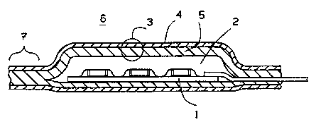
Figure 1 illustrates an electronic circuit l and a circuit-
5 ~.ULLUUI~dlng gas volume 2 enclosed by a casing 3. The casing 3
is comprised of a laminate which includes a metal foil 4 that
lies proximal to the ambient air 6, and a thermoplastic sheet
5 which lies proximal to the enclosed gas volume 2. The metal
~oil or sheet 4 and the t-hP L l~CtiC sheet or layer 5 adhere
10 effectively one to the other. The laminate from which the
casing 3 is formed is fusion-welded so as to form a joint
between the ~h~ ctic layers 5 on the inner surface of the
laminate 3, therewith sealing the casing 3 at joints 7. The
c,~yy~ c.s concentration of the gas volume 2 which encloses
15 the electrcnic circuit l, either completely or partially, is
80 low as to prevent the organic materials included in the
electrcnic circuit 1 or the thermoplastic layer 5 cf the
casing 3 frcm igniting even should a fault in the circuit 1
lead to u..cullLLulled and prnnmln~-Pd overheating of the
20 circuit. As a result of the metal foil 4 in the casing 3, air
is unable to di~fuse from the ambient air 6 into the gas
volume 2 between the electronic circuit 1 and the casing 3 in
an amount which wculd raise the oxygen concentration to a
level at which the material would ignite or a level at which
25 fire could be sustained in the event of overheating, this
prevention being effective during the lifetime of the electro-
nics. The gas imperviousness can be; uv~:d further by using
a laminate which includes several layers of metal fcil 4 and
intP ~ te plastic layers 5. The jointing zones are relati-
30 vely broad at the joins 7 and hence the diffusion path isrelatively long in comparison with the area at right angles to
the diffusion direction when oxygen-gas diffuses from the
ambient air 6 into the gas vclume 2 within the casing 3.
Consequently, the amount of air able to diffuse through the
35 joints is also insufficient to increase the oxygen con-
2 1 9 1 075
Wo 95l34347
centration to a level at which there is a danger of igllition
in the event of overheating, this preventative state of the
device prevailing during the lifetime of the electronics. In
the event of a fire in the ~uLLuul.dings, the outer metal-foil
-~ 5 covering of the casing 3 is sufficient to prevent ignition for
a rc~A~nnAhle length of time.
According to one variant of the described ` -~-r-nt, the
volume 2 ~uLLuu-.ding the electric circuit l and enclosed by
the casing 3 is filled, either completely or partially, with
an insulating liquid which functions to facilitate the
LL..~ uLL~tion of heat during normal working of the circuit 1
and to assist in maintaining a constant capsule volume in the
o~uLLt:.-ce of variations in pressure and t~ uLe. In the
case of this variant, the oxygen concentration in the ~olume
15 2 may not be so high as to cause oxygen-gas precipitation as
a result of heating and as a result of reduced solubility at
the elevated temperature, to an extent such that the amount of
oxygen gas present is able to sustain fire.
In the case of the l~mho~; - L illustrated in Figure 2, the
20 electronic circuit 1 is ~ULL~JUIlded by an oxygen-free gas
volume 2 and the casing 3 is comprised of a metal foil 4 and a
plastic layer S suitable for fusion-welding of the :lubsLLcl~e
layers to form the joints 7. There is provided on top o~ the
metal foil 4 a covering of plastic material 8 which in
25 combination with the ~h~-lly conductive metal foi~ 4 is
unable to sustain fire. Examples of such plastic material 8
are silicone elastomers which when burning in oxygen form a
suffocating outer layer of silicon dioxide. The outer plastic
material 8 may also include aluminium hydroxide, Al2û3 3li20, as
30 a filler which acts as an extinguishing agent by splitting
water when heated. Because aluminium oxide impairs electrical
properties, it cannot be used in immediate contact with the
electronics 1 and is therefore isolated from the electronics
1 and the ~uLLuullding gas volume 2 by the metal foil 4.
WOsS/34347 2 1 9 ~ ~75 F~~ u
In accordance with an alternative variant, the volume 2 is
filled either completely or partially with a solid material,
for instance a plastic material, that is able to fulfil the
same objects and requirements as those fl~lfillecl with the
5 liquid volume 2.
It will be understood that the invention is not restricted to
the aforedescribed and illustrated embodiments thereof and
that ~ rations can be made within the scope of the
following Claims.