Note: Descriptions are shown in the official language in which they were submitted.
WO95/24798 2 1 9 1 1 32 I~J/~ . 15
.
-- 1 --
THIN FILM ACTUATED MIRROR ARRAY FOR USE IN AN OPTICAL
F--" F ~ SYSTEM AND METHOD POR THE MANUFACTURE THEREOF
~E~TNI~ ~T FIEI.D OF THE INVENTION
The present invention relates to an optical
projection sy6tem; and, more particularly, to an array o~
M x N thin film actuated mirrors for use in the sy6tem and
method for the manufacture thereof.
BACK~ROUND ART
Among the various video di6play 6y6tem6 available in
the art, an optical pro]ection 6y6tem i6 known to be
15 capable of providing a high ~uality di6play in a large
6cale. In 6uch an optical projection 6y6tem, light from
a lamp i6 uniformly illuminated onto an array of, e . g., M
x N, actuated mirror6, wherein each of the mirror6 i6
coupled with each of the actuator6. The actuator6 may be
20 made of an electrodi6placive material 6uch e~s a
piezoelectric or an electro6trictive material which
deform6 in re6pon6e to an electric field applied thereto.
The reflected light beam from each of the mirror6 i6
incident upon an aperture of, e.g., an optical baffle. By
25 applying an electrical 6ignal to each of the actuator6,
the relative po6ition of each of the mirror6 to the
incident light beam i6 altered, thereby cau6ing a
deviation in the optical path of the ref lected beam f rom
each of the mirror6. A6 the optical path of each of the
30 reflected beams is varied, the amount of light reflected
from each of the mirror6 which pa6ses through the aperture
is changed, thereby modulating the intensity of the beam.
The modulated beams through the aperture are tran6nlitted
onto a projection screen via an appropriate optical device
35 such as a projection lens, to thereby di6play an image
WO95l14798 2 1 ~ 1 1 32 ~111 15
-- 2 -- -
thereon .
In Figs. 1 and 2, there are 6hown a cros6 sectional
and a perspective views, respectively, of an array 10 o~
M x N thin film actuated mirrors 11 for use in an optical
projection system, disclosed in a copending commonly owned
application, U.S. Ser. No. 08/340,762, entitled "ARRAY OF
THIN FILM ACTUATED NIRRORS FOR USE IN AN OPTICAL
PROJECTION SYSTEM AND NETHOD FOR THE MANUFACTURE THEREOF",
comprising an active matrix 12, an array 13 of M x N thin
lC film actuating structures 14, an array 15 of N x N
supporting members 16 and an array 17 of M x N mirror
layers 18.
The active matrix 12 includes a substrate 19, an
array of M x N transistors(not shown) and an array 20 of
M x N connecting term;nPl~ 21. Each of the actuating
structures 14 in the array 10 is provided with a first and
a second actuating parts 22(a), 22(b), the first and
second actuating parts 22(a), 22(b) being identically
structured, wherein each of the first and second actuating
parts 22(a), 22(b) has at least a thin film layer 23 of a
motion-inducing material , e . g ., piezoelectric material ,
including a top and a bottom surfaces 24, 25, an elastic
layer 26 having a bottom surface 26, and a first and a
second electrodes 28, 29. The elastic layer 29 i8 placed
on the bottom surface 21 of the motion-inducing thin ~ilm
layer 23. The first and second electrodes 28, 29 are
located on the top and bottom surfaces 24, 25 of the
motion-;n-ll-c;ng thin film layer 23, respectively, wherein
an electrical signal applied across the motion-inducing
thin film layer 23 located between the first and second
electrodes 28, 29 causes a deformation thereof, and hence
the actuating parts 22(a), 22(b). Each of the supporting
members 16 is used for holding each of the actuating
structures 13 in place and also for electrically
connecting each of the actuating structures 14 with the
WOgs/24798 2 ~ 91 132 r~ 15
.
- 3 -
~ctive m/~trix 12. Each of the mirror l~lyers ~8 incl~des
a first side 30, a second opposing side 31, and a c,enter
portion 32 therebetween as shown in Fig. 2, whereill the
first side 30 and the aecond opposing side 31 of each of
5 the mirror layers 18 are secured on top of the firs~ ~nd
second actuating parts 22(a), 22(b) of each of the
actuating structures 14, respectively, such that when the
first a~d second actuating parts 22 (a), 22 (b) in each of
the actuating structures 13 deform in response to the
10 electrical signal, the center portion 32 of the
L~ Iding mirror layer 18 tilts while I. ;n;nr~
planar, thereby allowing all of the center portion 32 to
reflect the light beams, resulting in an increased optical
ef f i ciency .
~here are a number of problems associated wit~ the
above-described thin film actuated mirror array 10. First
of all, each of the actuating structures 14, and hence,
the mirror layer 18 attached thereto, has a lin!lited
tilting angle . In the array l O, whenever each of the
20 actuating structures 14 tilts upward by more than 3~, a
part thereof is bound to come in contact with the active
matrix 12, thereby limiting the per~ormance thereof. In
addition, since the second electrode 29 partially covers
the bottom surface 25 of the motion-inducing layer 23 in
25 each of the actuating parts 22(a), 22(b) in each actuating
structure 14 to thereby leave portions of the mot:ion-
inducing layer 23 in a direct co~tact with the elastic
layer 2 6 and the respective materials making up the
elastic layer 26 and the motion inducing layer 23 are
30 provided with different thermal expansion coefficients, an
excessive level of stress may be developed between the
motion-;n~ ;n-J layer 23 and the elastic layer 26, leading
to an eventual separation thereof, which may, in turn,
lead to the formation of cracks or unevenness on each of
35 the mirror layers 18, thereby reducing the optical
Wo 95124798 ` 2 1 9 1 1 3 2 - -
-- 4 --
efficiency of the array 10.
DISCLQSURE QF 'r~ Nv~l~Llu~ _
S It is, therefore, a primary object of the present
invention to provide an array of M x N actuated mirrors
having an increased tilting angle.
It is another object of the present invent to provide
an array of M x N actuated mirrors having an increased
optical ~ff;~ ncy.
If is a further object of the present invention to
provide a method for manufacturing said array of M x N
actuated mirrors.
In accordance with one aspect of the present
invention, there is provided an array of M x N thin f ilm
actuated mirrors for use in an optical projection system,
said array comprising: an active matrix including a
substrate, an array of M x N transistors and an array of
M x N pairs of connecting tr~rminA~ wherein the
connecting terminals in each pair are electrically
connected to each of the transistors; an array of M x N
elastic members, each of the elastic me-m-bers being
provided with a distal and a proximal ends, and a top and
a bottom surfaces, the proximal end including a first tab
and a second tab portions, the first tab and second tab
portions being separated by a retraction therebetween, the
distal end including a protrusion, wherein the protrusion
f rom each of the elastic members extends into the
retraction of a successive elastic member in the array; an
array of M x N pairs of actuating structures, each pair of
the actuating structures being located on the f irst and
second tab portions on each of the elastic members,
respectively, each of the actuating structures including
a bias electrode, a motion-inducing thin fil~[l layer and a
signal electrode with the bias and the signal electrodes
WO 95/24798 2 1 9 ~ ~ 3 2
-- 5 --
being placed on top and bottom of the motion-induciny thin
ilm layer, respectively, the bias electrode being ma.de o~
an electrically rfmtl~ ;n~, light re1ecting materia~., the
signal electrode in each of the actuating structures in
5 each pair being electrically connected to a same
transistor in the active matrix, wherein an electrical
signal applied across the motion-in~lllr;n~ thin film layer
between the bias and the signal electrodes in each of the
actuating structures causes a deformation of the motion-
10 inducing thin film layer, and hence, said each of theactuating structures; an array of M x N pairs of
supporting members, each pair o the supporting members
being used for holding each of the elastic members in
place, wherein the first and second tab portions in each
15 of the elastic members are secured to each of the
supporting members in each pair, respectively; an array of
M x N mirrors or r~f 1 ~rt i nrJ light beams, each of the
mirrors being formed on the top surface of the elastic
member, each of the mirrors being made of the same
20 material as the bias electrode, such that when the pair of
actuating structures deform in response to the electrical
signal, the first and second tab portions on the elastic
member with the actuating structures attached thereto tilt
while the r. 1nri~r of the elastic member, and, henc~, the
25 mirror formed on top thereof, stays planar, thereby
allowing all of the mirror in its entirety to reflect the
light beams.
In accordance with another aspect of the presellt
invention, there is provided a method for manufacturing an
30 array of M x N thin film actuated mirrors for use in an
optical pro~ection system, said method comprising the
steps of: a) providing an active matrix having a top
surface, the active matrix including a substrate, an array
o M x N transistors and an array of M x N pairs o~
35 connecting t~rm;n~l~ on the top surface thereof; b)
.
Wo 95/24798 2 1 9 1 1 3 2 1 ~1~ s ~ AS
.
-- 6 --
forming a sacrlficial layer on the top surface of the
active matrix in such a way that the sacrif icial layer
completely covers the array of M x N pairs of connectillg
tPrminA1 c; c) removing the sacrificial layer surrounding
5 each of the c~nnPc~;n~ tPrm;nAl c; d) forming a supporting
member around each of the connecting tprm; nA l ~; e )
depositing an elastic layer on top of the sacrif isial
lAyer and supporting members; f ) forming an array of M x
N pairs of conduits, each of the conduits extending f ron,
10 top of the elastic layer to each of the connecting
rm;nAl~ via each of the supporting members; g) providin~
an array of M x N pairs of signal electrodes on top of the
elastic layer in such a way that each of the signal
electrodes is in contact with each of the conduits and
15 hence each of the connecting terminals; h) forming a
motion-inducing thin film layer on top of each of the
signal electrodes; i ) depositing a layer made of an
electrically conducting light ref lecting material on top
of the motion ;n~ ;n~ and elastic layers to tkereby form
20 a s-om;f;n;ch~; array of actuated mirror structures; j)
patterning the 5P~;f;n;chPrl array of actuated mirror
structures into an array of M x N actuated mirror
6tructures, each of the actuated mirror structure6
including a pair of 6upporting member6, a 6acrif icial
25 layer, an ela6tic member with a pair of actuatins
structure6 and a mirror made of the electrically
~ n~l~r~;n~, light reflecting material formed on top
thereof, each of the actuating structures having a bias
electrode made of the electrically conducting, light
30 reflecting material, the motion-inducing thin film layer
and the signal electrode, the elastic member further being
provided with a distal and a proximal ends, and a top and
bottom surf aces, the proximal end including a f irst tab
and a second tab portions, the first and second tab
35 portions being separated by a retraction therebetween, the
W095124798 21 91 1 32 r~" r
- 7 -
distal end including a protrusion, each of the act~1ating
structures being placed on top of the first and seco]1d tab
portions, respectively, wherein the protrusion from each
of the elastic members, and hence, the actuated mirror
5 structures, extends into the retraction of a successive
elastic member, and hence, a successive actuated mirror
structure, in the array; and k) removing the sacrificial
layer to thereby form said array M x N thin film actuated
mirrors .
BRIEF DESCRIPTION ~F THE DRAWINGS
The above and other objects and features of the
present invention will become apparent from the fol]owing
15 description of preferred embodiments given in conjunction
with the accompanying drawings, wherein:
Fig. 1 shows a cross sectional view of an array of M
x N thin film actuated mirrors previously disclosecl;
Fig. 2 discloses a perspective view of a thin film
20 actuated mirror constituting the array shown in FicJ. l;
Fig. 3 represents a cross sectional view of an array
of M x N thin film actuated mirrors in accordance with a
preferred embodiment of the present invention;
Fig. 4 depicts a detailed cross sectional vie~ of a
25 thin film actuated mirror constituting the array shown in
Fig. 2;
Fig. 5 illustrates a top view of the thin film
actuated mirror shown in Fig. 3;
Fig. 6 presents a top view of an a thin film actuated
30 mirror in accordance with another preferred embodiment of
the present invention; and
Fig6. 7A to 7J reproduce 6chematic cross sectional
views setting forth the manufacturing steps for the first
embodiment in accordance with the present invention.
.
W09s/24~98 ` 2 1 9 1 ;~ S
- 8 - l 2
MODES OF ÇhRRYING OUT ~ INVENTION
Ref erring now to Figs . 3 to 7, there are provided
schematic cross sectio~al and top views of the inventive
5 array of M x N thin film actuated mirrors for U8~ in an
opticr~l projection system and method for the manufacture
thereof, wherein M and N are integers, in accordance with
preferred embodiments of the present invention. It should
be noted that like parts appearing in Figs. 3 to 7 are
10 represented by like refere~ce numerals.
In Fig. 3, there is illustrated a cross sectional
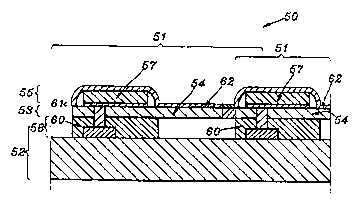
view of a first embodiment of an array 50 of M x N t~i
film actuated mirrors 51, comprising an active matrix 52,
an array 53 of N x N elastic members 54, an array 55 of M
15 x N pairs of actuating structures 57, an array 58 of M x
N pairs of supporting members 60 and an array 61 of M x N
mirrors 62.
Figs. 4 and 5 represent a detailed cro~G sectional
and a top view of a thin f ilm actuated mirror 51
20 constituting the array 50 shown in Fig. 3. The active
matrix 52 includes a substrate 63, an array of M x N
transistors(not shown) and an array 64 of M x N pairs of
connecting terminals 66, wherein the connecting terminals
66 in each pair are ~ r~ri~ Al ly connec~ced to each of the
25 transistors. Each of the elastic members 54, having a
thickness of 0.7 - 2,um and made of a ceramic, ~e.g., Si3N4,
5iO2 or poly-Si, is provided with a distal and a proximal
ends, 67, 68 and a top and a bottom surfaces 6g, 70. Th~
proximal end 68 includes a first tab and a second tab
30 portions 71, 72, the first and second tab portions being
separated by a retraction 73 therebetween, and the distal
end 67 includes a protrusion 74, wherein the protrusion 74
from each of the elastic members 54 extends into the
retraction 73 of a successive elastic members 54, as shown
35 in Fig. 5.
W095124798 21 91 1 32 r~". . Is
Each of the actuating structures 57 in each pair i8
located on the first and second tab portions 71, 72 on
each of the elastic members 54, respectively, and includes
a bias electrode 77, a motion-inducing thin film layer 75
5 ~nd el signal electrode 76 with the bias and signal
electrodes 77, 76 being placed on top end bottom of the
motion-in~ c;n~ thin film layer 75. The bias electrod~
77, having a thickness of 500 - 2000A, is made of ar
electrically conducting, light reflecting material, e.g.,
10 silver(Ag) or aluminum(Al), the signal electrode 76,
having a thickness of 500 - 2000A, is made of an
electrically conducting material, e.g., platinum~Pt~ or
platinum/titanium(Pt/Ti), and the motion-inducing thin
film layer, having a thickness of 0 . 7 - 2ym, is made of a
15 piezoelectric material, e.g., barium titanate (BaTiO3), or
an electrostrictive material, e.g., lead magnesium niobat~
( PMN ), respectively .
An insulation 106 formed around each of the signal
electrodes 76 and the motion-inducing layer 75 on top
20 thereof prevent the bias electrode 77 from coming in
contact with the signal electrode 76. When an electrica~
signal is applied across the motion-inducing thin film
layer 75 between the bias and signal electrode 77, 76 in
each of the actuating structures 57, it results in a
25 deformation of the motion-;n-lllc ;n~ thin film layer 75, and
hence the actuating structure 57.
Each pair of supporting members 60, made of a
ceramic, e.g., Si3~4, sio2 or poly-Si, is used for holding
each of the elastic members 54 in place and also for
30 electrically connecting the signal electrode 76 in each of
actuating structures 57 on the elastic member 54 with th~
corresponding cnnnP~;n~ tPrm;nAl 66 on the active matrix
52. The first and second tab portions 71, 72 in eac~l of
the elastic members 54 are cantilevered from each of the
35 supporting members 60 in each pair, respectively. Each
Wo95/24798 2 1 9 1 1 32 1~1/. s .~
-- 1 o
of the supporting members 60 includes a conduit 80 for
transmitting the electrical signal to the signal electrode
76, made of a metal, e.g., tungsten(W), and extending from
top of the elastic member 54 to the correspondiny
connecting terminal 66. The mirror 62 in each of the
actuated mirrors 51 is made of the same material as the
bias electrode 77 and is formed on top of the elastic
member 54. In other word, the electrically conducting,
light reflecting material deposited on the ela6tic member
54 functions as the bias electrode 77 and also as the
mirror 6 2 .
In each of the thin film actuated mirrors 51, each Qf
the actuating structures 57 i6 located on top of tlle first
and second tab portions 71, 72, respectively, such that
when each of the actuating structures 57 deforms in
response to the electrical signal, the tab portions 71, 72
with the actuating structures 57 attached on top thereof
bend while the L. ;n~l~r of elastic member 54 remains
planar thereby allowing all of the mirror 62 on top
thereof to ref lect the llght beams .
In Fig. 6,~there is illustrated top view of a thin
f ilm actuated mirror 10 0 in accordance with another
pref erred ~ ` 1; 1 of the present invention . ~he thin
film actuated mirror lO0 is similar to the thin film
actuated mirrors 51 previously described except that it is
provided with an elastic member 54 which is
configurationally different, and hence, a mirror which is
configurationally different. The elastic member 54 is
provided with a first, a second and a cen~er tab por~ions
71, 72, 83 at the proximal end 68 thereof, wherein the
f irst, second and center tab portions are separated by a
gap 84 therebetween.
In the thin film actuated mirror 51 of the first
embodiment or the thin film actuated mirror 100 of the
second '~ , a pair of actuating structures 57 are
W09sl24798 2 ~ 9 ~ ~ 32 1~1/~ c -
located only on the tab portions, and the mirror 62 is
formed direc~ly on the elastic member 54, and therefore
there is less l;k~l;h~od of a stress developing and hence
less 1 ;k.ol ;h-~od of cracks forming on the mirror 62.
5 Furthermore, since the pair of actuating structures 57 is
located only on the tab portions 72, 73 of the ela6tic
member 54 in the first: ` o~l;r t or in the second
embodiment, the actuated mirror 51, 100 in either
.= ' _'; Ls will not come in contact with the active
10 matrix 52, even if the actuated structures 14 bend upward
by more than 3 .
There are illustrated in Fig. 7A to 7J the
manufacturing steps involved in manufacturing of the first
embodiment of the present invention. The proces~, for
15 manufacturing the first embodiment, i.e., the array 50 o
M x N thin f ilm actuated mirrors 51, begins Wit~l the
preparation of the active matrix 52 having a top surface
101, comprising the substrate 63, the array of M x N
transistors(not shown) and the array 64 of M x N pairs
20 of connecting t~rm;n~l ~ 66, as shown in Fig. 7A.
In the subsequent step, there is formed on the top
surface 101 of the active matrix 52 a sacrificial layer
102, having a thickness of 1 - 211m and made of a m~tal,
e.g., copper (Cu) or nickel(Ni), or phosphor-silicate
2~ glass(PSG) or poly-Si, by using a sputtering method if the
sacrificial layer 102 is made of a metal, a chemical vapor
deposition (CVD) or a spin coating method if the
sacrificial layer 102 is made of PSG, and a (CVD) m~thod
if the sacrificial layer 102 is made of poly-Si, as
30 illustrated in Fig. 7B.
Subsequently, there is formed a first sUpportins
layer 103 including the array 58 of M x N pairs o~
supporting members 60 and the sacrificial layer 102,
wherein the first supporting layer 103 is formed by:
35 forming an array of M x N pairs of empty slots (not s]lown)
Wo 95/24~98 2 1 9 1 1 3 2 A ~ .,, l5
-- 12 --
using a photilithography method, each of the empty slots
being located around each of the connecting termin~l6 66;
and forming a supporting member 60, made of a ceramic,
e.g., Si3N4, SiOz or poly-Si, in each of the empty slots
5 located around each of the -~7nnect;n~ terminals 66, using
a sputtering method or a CVD method, as shown in Fig. 7C.
Thereafter, an elastic layer 105, made of the same
material as the supporting member 60 and having a
thickness of 0.7 - 2~m, is formed on top of the first
10 supporting layer 103, as depicted in Fig. 7D. It should
be noted that the formation of the supporting members 60
and the elastic layer 105 can be combined in a single
step. The sacrificial layer ~102 in the first supporting
member 103 is then treated as to be removable later by
15 using an etching method or by applying appropriate
chemicals .
The conduit 80 for electrically connecting the slgnal
electrode 76 in each of the actuating structures 57 with
the corresponding connecting terminal 66, made of a metal,
20 e.g., tungsten(W) or titanium(Ti), is formed in each of
the supporting member 60 by first creating a hole
extending from top of the elastic layer lQ5 to top of th~
respective connecting terminal 66, using an etcl~ g
method, followed by filling therein ~ith a metal, e.~., W,
25 as depicted in Fig. 7E.
Subsequently, as shown in Fig. 7F, a signal electrode
76, made of an electrically conducting material, e.g., Pt,
and having a thickness of 500 - 2000A, is formed on top oE
each conduit 80 using a sputtering method. Each of the
30 si~n~ ro~les 76 is electrically connected to each of
the connecting tF~rm;n~l~ 66 through the conduit 80. In
the subsequent step, a thin film motion=inducing layer 75,
made of ~ piezoelectric material , e . g ., BaTiO3 , or a
electrostrictive material, e.g., PMN and having a
35 thickness of 0.7 - 211m, is formed on top of each of the
W0 9s/24798 2 1 9 7 1 3 2 r~ A5
.
-- 13 --
signal electrodes 76 using a sol-gel method or a
aputtering method, and then it i8 heat treated to allow a
phase transition thereof to take place. Since the motion-
inducing thin film layer 75 is sllff;r;-~ntly thin, there is
5 no need to pole it: it can be poled with the electrical
signal applied during the operation thereof.
Thereafter, each of the signal electrode 76 and the
motion-;n~l--r;n~ thin film layer 75 formed on top thereo~
are covered with the same material as the elastic layer
10 105, and portion thereof is then removed to expose top of
the motion inducing layer 76, thereby forming cm
insulation 106 around each of the signal eLectrodes 76 and
the motion-;nrll-rinr~ layer 75 formed thereon, as depicted
in Fig . 7G .
lS Subsequently, a layer 107 made of an electrically
conducting, light reflecting material, e.g., Al, and
having a thickness of 500 - loOOA, is formed on top of the
motion- ;nr~l1ring and elastic layers 75, 105 to form a
g~rn;f;n;~hed array 108 of actuated mirror structures 10~
20 using a sputtering or a vacuum evaporation method. This
layer will function as the bias electrode 77 and mirror 62
in the thin film actuated mirror 51, as shown in Fig. 7H.
The insulation 106 formed around each of the signal
electrodes 76 and the motion-inducing layer 75 on top
25 thereof prevent the bias electrode 77 from coming in
contact with the signal electrode 76.
Thereafter, as shown in Fig. 7I, the semifinishod
array 108 of actuated mirror structure 109 i9 then
patterned into an array 110 of M x N actuated mirror
30 structures 111 using a dry etching method, or
photolithography method, each of the actuated mirror
structures 111 ;nrlll-l;nrJ on elastic member 54 with a pair
of actuating structures 57 and a mirror 62 made of the
electrically conducting, light reflecting material formed
35 on top thereof, each of the actuating structures 57 havlng
w0 95/24798
-- 14 --
a bias electrode 77 made of the electrically conducting,
light reflecting material, a motion-;n~ ing thin film
layer 75 and a signal electrode 76, the elastic member 54
iurther being provided with a distal and a proximal ends
67, 68, and a top and bottom surfaces 69, 70, the proximal
end 67 including a first tab and a second tab portions 71,
72, the first and second tab portions 71, 72 being
separated by a retraction 73 therebetween, the distal end
67 including a protrusion 74, each of the actuating
6tructures 57 being placed on top of the first and second
tab portion6 71, 72, respectively, wherein the protrusion
74 from each of the elastic members 54, and hence, the
mirror 62, extends into the retraction 73 of a successive
electric members 54.
The sacrificial layer is then removed by using dn
etching method to thereby form the array 50 of. ~q x N thin
f ilm actuated mirrors 51 as depicted in Fig . 7J .
The method used in manufacturing of the second
t involves similar gteps except that it involves
a different patterning of the cr~l;f;n;cll~rl array 108 of
actuated mirror structures 109.
While the present invention has been described with
respect to certain preferred: lo~l; ts only, other
modifications and variations may be made without departing
from the scope of the present invention as set forth in
the following claims.