Note: Descriptions are shown in the official language in which they were submitted.
2191339
Method and Device for Continuous D'niform
Electrolytic Metallisiag or Stchiag
Description
The invention relates to a method and a device in
particular for continuous uniform electrolytic
metallising or etching of metal surfaces.
Methods of metallising or etching, particularly for
processing and manufacturing printed circuit boards,
and devices suitable for this purpose have been known
for a long time. For example there is described in DE
36 24 481 A1 an arrangement for electrolytic
application of a metal to plate-shaped articles such as
printed circuit boards, in which these articles are
brought into an electrolysis bath for a certain
residence time and are then removed from the bath, the
articles being supplied in a horizontal position to an
electrolysis chamber forming the arrangement, being
passed continuously through this and after electrolytic
treatment are brought out of the chamber again, and in
which anodes, power supplies and transport means are
provided. The transport means are further in the form
of an endlessly revolving driven series of individual
transport members, which securely hold the lateral
edges of the plate-shaped articles and move them in the
direction of travel, and in which at the beginning and
end of the transport path situated in the electrolysis
2191339 2
chamber, means are provided which cause the articles to
be grasped by the transport members or released by
them. Such an installation can be used with
corresponding additional equipment also for
electrolytic etching for example the removal of metal
coatings (demetallising?.
In other arrangements, the articles to be treated are
dipped in a vertical position into a treatment agent or
are brought into contact therewith by spraying or
injection, the counter electrodes necessary for the
electrolytic treatment being located opposite the said
article_ For electrolytic metallisation, the counter
electrodes are polarised as anodes and for an etching
process as cathodes.
In the known electrolytic installations in which the
articles are disposed horizontally and are moved in a
horizontal direction through the arrangement, the
spacing between the articles and the counter electrodes
comes to approximately 100 mm. In the manufacture of
printed circuit boards, such large spacings have a
detrimental effect on the quality of the coatings to be
processed. Narrow conductor strips on the printed
circuit boards act relative to adjacent wide conductor
strips as peaks, on which the electrical field in the
electrolytic treatment cell is concentrated. Therefore
a higher localised current density forms at these
points, so that these points are thus more intensively,
2191339 3
i.e. more rapidly electrolytically etched or metallised
than wide conductor strips.
as a result coating thickness ratios of z:3 and more
are encountered at the various points on the surface of
a printed circuit board. During etching, the different
electrical field intensities lead to an attack on the
lateral flanks of a conductor strip and thus to under-
etching. This is no longer tolerable in fine conductor
technology, in which conductor strip widths of 0.1 mm
and less are to be produced.
In order to solve this problem various measures are
possible, individually or in combination. Thus for
25 example the electrolytic treatment may be carried out
at a low current density. However, in this way the
efficiency of the treatment installation is reduced.
Improvements are also achieved with an enlarged spacing
between anode and cathode. On the other hand, the peak
effect described may also be avoided in that the
spacing between anode and cathode is reduced so far
that the narrow conductor strips no longer act as
peaks, but as surfaces. This is the case particularly
when the counter-electrodes (during etching the
cathodes, and during metallising the anodes) are
brought closer to the articles for treatment to a
spacing of 1 mm or Less. In this case the maximum
usable current density is limited only by the required
quality of the metal coatings to be processed or
CA 02191339 2004-07-26
4
produced and the thickness-specific surfaces of the
diffusion layer, which in turn is influenced by the
intensity of the convection of the electrolyte at the
treatment point. The maximum current density lies
5 considerably above the current density which is usable
in conductor strips which act as peaks. Thus an
electrolytic treatment with extremely small spacings
between anode and cathode is preferred.
10 Such devices, which are used for example for treating
strip-like carrier materials or metal strips, are
described in DE-OS 25 11 336 and EP 0 264 510 A1.
Small spaces between the anodes and cathodes may be
produced in particular with roller-shaped electrodes
which roll along the surface of the material for
treatment. Such an arrangement is described in w0
94/03655.
20 In order to avoid electrical short circuits, in this
case an insulating spacer means is provided between the
roller-shaped electrodes and the article to be treated.
Suitable for this are for example partial coatings of
the rollers, which are so constructed that the current
25 permeability is extensively maintained by the film of
fluid lying between the rollers and the material for
treatment. It is also possible to use the resist
applied to the surface of the printed circuit boards,
CA 02191339 2004-07-26
5
said resist representing the conductor image as
positive or negative, as spacing means. This latter is
electrically insulating and its coating thickness is of
such a size that short circuits are reliably avoided.
5
Such rollers may for example be in the form of
insoluble electrodes. For electrical contacting these,
due to the rotating, must be electrically conductively
connected via slip rings and slip brushes to the source
10 of bath current. This slip ring technique is however
technically complex. Such arrangements are shown in
German Patents DE 44 17 550 CA and DE 44 17 551 A1. In
these, for example, electrically non-conductive spacer
rings are used as insulating spacer means on the
15 roller, or the insulating layer of a photoresist on the
surface of the printed circuit board surface for
contacting, slip contact brushes are used, attached to
slip rings on the rollers to be contacted.
20 A device and method are known from US-A-3619386 by
means of which metal films can be electrolytically
deposited. A non-electrically-contacted bipolar
activating electrode is in the form of a belt passes
around two rollers and continuously contacting the
2191339
6
cathode surface under pressure. In this case the
surface of the belt passes over an anode and a
cathode, depositing on the cathode surface metal
dissolved from the anode and carried along by the
belt. The surface of the belt includes metal and
bound up therewith electrically non-conductive
particles of Knoop hardness H 10 according to ASTI.
The particles have an abrasive action on the cathode
surface, and are therefore unsuitable for treatment
of printed circuit boards. The method is designed
as a high-current process and therefore has the
disadvantage already described, i.e. of forming
current peaks with the conductor tracks. In
electrolytic etching according to known methods and
arrangements, the slip-ring technique is also
necessary in order to connect the insoluble roller-
shaped electrode to the source of bath current. If
the roller-shaped electrode is located between the
material for treatment and an electrode lying
opposite the said material, metal deposits on this
electrode both in electrolytic etching and in
metallisation, in metallisation on the side facing
away from the material for treatment, and in etching
on the side of the roller facing the said material.
Therefore the metal has to be removed from this
electrode, continuously or chronologically repeated
treatment cycles. For continuous removal a second
source of bath current is suitable, which
2191339
6a
positively polarized relative to the electrode
during metallisation, and during etching is
negatively polarised relative to the electrode. For
example the material for treatment, a printed
circuit board, can be conveyed in a horizontal
position and in a horizontal direction through a
treatment installation. The roller-shaped
electrode, which is electrically conductive at least
on its surface, Bolls along the surface of the
material for treatment, an insulating spacer means
being provided, which avoids an electrical short
circuit between the electrode and the material for
treatment.
During etching, the positive pole of the source of
current is electrically connected in a way known per
se with the material for treatment, for example via
electrically contacting clamps. The negative pole
is connected to the electrode via a slip contact and
a slip ring. The etched-off metal is deposited on
the said electrode. A second electrolytic cell is
formed by a further source of bath current, the
electrode and
~
2191339
a further auxiliary electrode, the second cell being
disposed on the side of the electrode facing away from
the material for treatment. The positive pole of the
second source of bath current is connected via the same
slip contact and slip ring with the electrode as the
negative pole of the first source of bath current and
its negative pole with the electrode lying opposite the
material for treatment. The metal is deposited on this
latter, said metal being again dissolved from the
electrode again after the material for treatment has
been etched_
Should metal deposited on the electrode during
metallisation not be entirely removed again, this can
i5 be etched off, the polarity of the sources of bath
current being intermittently changed in a way known
per se, and plates having insoluble metal surfaces
being also treated in the installation. In this case
the metal dissolves again from the electrodes and
deposits on the counter-electrodes, which in this case
are incorporated cathodically, so that no further metal
is deposited on the electrodes.
In such methods, the electrode must be electrically
contacted via slip contacts. This is constructively
complex and requires intensive servicing. Furthermore,
an additional source of bath current is required.
lagain, the treatment method for removing the metal
21913398
deposited on the electrodes must be interrupted from
time to time.
Instead of an insoluble counter-electrode, basically
S soluble or at least partly soluble counter-electrodes
may also be used. In this case however, suitable
measures must be taken in order to keep constant the
metal ion concentration in the electrolyte fluid. In
the case of metallisation of the material for
treatment, for this purpose for example salts of the
metal to be separated are added. During etching, these
must be removed again from the electrolyte by suitable
methods. A continuous supplementation of the metal
salts results in a continuous consumption of metal
salts, decomposition products thereby being
continuously enriched in the electrolyte, and requiring
to be removed in a complex manner-from the electrolyte
and disposed of. The use of cost-effective soluble
electrodes is not possible, because these, due to their
dissolution, are not dimensionally stable, and
therefore do not permit a constant small effective
distance between anode and cathode.
In view of this, the problem underlying the present
invention is to find a method of continuous uniform
electrolytic metallisation of etching (demetallising)
of metal surfaces, particularly also of printed circuit
boards, and a device suitable for carrying out such a
method. In particular, disadvantages of the known
CA 02191339 2004-07-26
9
methods and arrangements are to be avoided, while still
utilising their advantages.
The term metal surface is understood to mean also a
surface of non-metallic material, which is at least
partly coated with metal.
In the method according to the invention in particular,
small effective distances are made possible between the
anodes and cathodes, so that extremely uniform metal
coatings can be obtained on printed circuit boards with
narrow and wide conductive tracks. Soluble anodes are
used as counter-electrodes for continuous metallisation.
Supplementation of the metal ions by addition of metal
salts to the electrolytic fluid is not necessary. In
electrolytic etching the metallisation for example is not
interrupted during the manufacture of printed circuit
boards by cyclical demetallisation procedures on the
electrodes. In addition the arrangement according to the
invention is simple in construction and requires no
complex outlay on servicing, as there is no necessity to
use a complicated slip contact technique for rotating
roller electrodes. In the device according to the
invention electrodes formed from the metallic surfaces of
2191339 10
Plates in particular can be used as counter-electrodes.
The source of bath current is connected to these
electrodes. Between the material for treatment and the
counter-electrodes there are located movable, for
example rotating roller-shaped electrodes, which are
not connected to the source of bath current. The
spacing between the material for treatment and the
counter-electrodes is extensively bridged over by these
intermediate electrodes. The intermediate electrodes
are electrically conductive. They are however mounted
in an electrically insulated manner and for example
move in a rolling fashion at a very small distance from
the surfaces of the material for treatment. In one
embodiment of the invention the intermediate electrodes
can also contact the surfaces of the material for
treatment is a wiping manner, their speed of movement
or rotation being adjusted relative to the surface of
the material for treatment in an appropriate way.
In order to avoid direct metallic contact between the
material for treatment and the metallic surface of the
intermediate electrodes, there are located therebetween
electrically insulating spacer means, which are
permeable to liquid and ions, for example ceramic
particles or partial plastics coatings, textile
structures or plastics rings or other profiled
material, on the outer side of the intermediate
electrode_ Their shape and arrangement are so selected
that the electrical field lines can pass substantially
2191339
unhindered through the thin film of liquid located
between the intermediate electrodes and the material
for treatment. The electrical screening effect of
these spacer means is small. For example, screening
effects of the individual spacer means can be
compensated for if the spacer means are located on
rollers disposed along the direction of transport in
the treatment installation, and offset to one another.
The intermediate electrode is preferably constructed
from an insoluble material, for example of stainless
steel or titanium with or without a coating of noble
metals or their oxides.
The spacing between the intermediate electrodes and the
counter-electrode is of such dimensions that here also
any contact is reliably avoided.
Such intermediate electrodes disposed in an insulated
manner-between the material for treatment and the
electrodes are metallised on the side facing the anode,
and demetallised, i.e. etched, on the side facing the
cathode. During metallisation of the material for
treatment, therefore, metal is deposited on the side of
the intezmediate electrode facing away from the
material for treatment, and during etching on the side
facing the material for treatment.
sy means of suitable construction, the intermediate
electrodes can also serve to transport treatment fluid
CA 02191339 2004-07-26
12
on to the surface of the material for treatement.
For this purpose the intermediate electrodes may for
example consist of an open-work inner tube and a
metal mesh surrounding this latter, for uniform
5 distribution of the emerging treatment medium.
Suitable embodiments for such roller-shaped
electrodes are described in WO 94/03655 and in WO
9520692 A1.
10 According to one aspect of the invention, there is
provided a method of uniform electrolytic
metallising, etching or demetallising of at least
one metal surface, in which: the at least one metal
surface and at least one electrode lying opposite
15 the at least one metal surface are brought into
contact with a metallising, etching or demetallizing
treatment medium; an electrical voltage is applied
between the at least one metal surface and the at
least one electrode; there is disposed between the
20 at least one metal surface and the at least one
electrode at least one electrically uncontacted,
insoluble intermediate electrode containing at least
on the outer side an electrically conductive
material, said at least one intermediate electrode
25 rolling with a small spacing from the at least one
CA 02191339 2004-07-26
12a
metal surface or the at least one intermediate
electrode is in wiping contact with the at least one
metal surface through an electrically insulating
intermediate layer being introduced between the at
5 least one intermediate electrode and the at least
one metal surface and not directly, and the speed of
movement of the at least one intermediate electrode
relative to the at least one metal surface is set in
a manner to achieve metallizing, etching or
10 demetalisition
According to another aspect of the invention, there
is provided a device for continuous uniform
electrolytic metallisation or etching of at least
15 one metal surface on a printed circuit board,
comprising: the at least one metal surface; at least
one electrode lying opposite the at least one metal
surface; a metallising, etching or demetallilzing
treatment medium in contact with the at least one
20 metal surface and the electrodes; a source of
voltage in contact with the at least one metal
surface and the at least one electrode; and
at least one electrically uncontacted, rotatable,
insoluble intermediate electrode disposed between
25 the at least one metal surface and the at least one
CA 02191339 2004-07-26
12b
electrode, containing at least on the outer side an
electrically conductive material, said at least one
intermediate electrode rolling with a small spacing
from the at least one metal surface, or the at least
5 one intermediate electrode is in wiping contact with
the at least one metal surface through an
electrically insulating intermediate layer between
the at least one intermediate electrode and the at
least one metal surface and not directly, and the
10 speed of movement of the at least one intermediate
electrode relative to the at least one metal surface
is set in a manner as to achieve metallizing,
etching or demetalisition.
15 According to yet another aspect of the invention,
there is provided a method for the continuous,
uniform, electrolytic metallization or etching of at
least one metal surface on a printed circuit board
or conductor foil, wherein: the at least one metal
20 surface and at one electrodesituated opposite said
at least one surface are brought into contact with a
metallising, etching or demetallizing treatment
agent; an electrical voltage is applied between the
at least one metal surface and the at least one
25 electrodes and at least one electrically non-
CA 02191339 2004-07-26
12c
contacted, insoluble intermediate electrodeformed
from an electrically-conductive material at least at
portions of the external surfacethereof is disposed
between the at least one metal surface and the at
5 least one electrode and travels at a small spacing
from the at least one metal surface; or at least one
electically non-contacted, insoluable intermediate
electrode is in wiping contact with the at least one
metal surface, an electrically insulating
10 intermediate layer being introduced between the at
least one intermediate electrode and the at least
one metal surface, and the speed of movement of the
intermediate electrode relative to the at least one
metal surface is set in a manner as to achieve
15 metallising, etching or demetalisition.
According to a further aspect of the invention,
there is provided an apparatus for the continuous,
uniform, electrolytic metallization or etching of at
20 least one metal surface on printed circuit board or
conductor foil, comprising: the at least one metal
surface; at least one electrode situated opposite
said at least one surface; a metallising, etching or
demetallizing treatment agent which is in contact
25 with the at least one metal surface and the at least
CA 02191339 2004-07-26
12d
one electrode; a voltage source which is in
electrical contact with the at least one metal
surface and the at least one electrode; and
at least one electrically non-contacted, insoluble,
5 rotatable intermediate electrode disposed between
the at least one metal surface and the at least one
electrode and formed from an electrically conductive
material, at least at portions of the external
surface thereof, said at least one intermediate
10 electrode being provided externally with an
electrically insulating intermediate layer and being
configured as a roller.
According to a further aspect of the invention,
15 there is provided a method of uniform electrolytic
metallizing, etching or demetallizing of a metal
surface, comprising: bringing the metal surface and
at least one electrode lying opposite it into
contact with an electrolyte; applying an electrical
20 voltage between the metal surface and the at least
one electrode; positioning between the at least one
electrode and the metal surface at least one
electrically unconnected insoluble intermediate
member comprising a roller with an electrically
25 conductive material on at least a part of its outer
CA 02191339 2004-07-26
12e
surface, and rolling each intermediate member along
the metal surface, each intermediate member acting
as a bipolar electrode; wherein at least one
electrically insulating member is interposed between
5 each intermediate member and the metal surface to
form a gap between each intermediate member and the
metal surface.
In a further aspect of the invention, there is
10 provided a device for continuous uniform
electrolytic metallizing, etching or demetallizing
of a metal surface, comprising: an electrolysis
cell; at least one electrode and means to position
the metal surface opposite the at least one
15 electrode; an electrolyte in the electrolysis cell
adapted to contact the metal surface and the at
least one electrode; a source of voltage and means
to connect the source of voltage with the metal
surface and the at least one electrode; at least one
20 electrically unconnected insoluble movable
intermediate member comprising a roller with an-
electrically conductive material on at least part of
its outer surface disposed between the metal surface
and the at least one electrode and adapted to serve
CA 02191339 2004-07-26
12f
as a bipolar electrode; means for rolling each
intermediate member along the metal surface; and
at least one electrically insulating member
interposed between each intermediate member and the
5 metal surface to form a gap between each
intermediate member and the metal surface.
The present invention will be illustrated and
described in theory an by way of example with
10 reference to the diagrammatic Figures, but without
restricting the invention thereto. Shown are:
Figure 1: a device not according to the invention,
showing only the theoretical effect;
15 Figure 2: a theoretical view of an etching process
according to the invention;
Figure 3: a theoretical view of the metallisation
process according to the invention.
20 For reasons of simplicity of drawing, the devices
are not shown true to scale.
According to Figure 1 there are located in a bath
container 9 with electrolyte liquid 10 a cathode 11
CA 02191339 2004-07-26
12g
and an anode 12. A source of bath current 13 is
electrically connected to the anode and to the
CA 02191339 2004-07-26
13
cathode. If an electrical conductor, in this case a
part provided with a metallic surface or a metal
part 14, which has no contact with the anode or the
cathode, is introduced into the anode/cathode path
5 when the source of bath current is switched on, then
in the area 15 of the part metal is deposited, which
has dissolved from the anode due to the electrolysis
procedure. If the metal part 14 itself is soluble,
metal is electrolytically removed from the area 16
of the part and deposited on the cathode 11. If on
the other hand the metal part in the electrolyte
fluid is insoluble, then gas is generated at the
area 16 facing the cathode.
The reference numeral 17 represents an axis about
which the metal part can be rotated. After a
rotation of 180° of the metal part in the direction
of arrow 18, the metal deposited in area 15 is now
opposite the cathode. Here it is etched off again
an finally deposited on the cathode. At the same
time metal etched off is now separated from the
anode in the area 16. This procedure is repeated,
with corresponding relative movement to the
electrc.3es, for example with continous rotation of
20 the metal part.
w 2191339
13a
The flow of electrolyte through the aon-electrically
contacted metal part comes about due to the very
varying electrical conductivities of the electrolyte
21913394
fluid and of the metal part. The metal part serves as
a metal conductor between the electrodes, the cathode
11 and the anode 12. This intermediate member thus
involves an intermediate electrode. In a preferred
embodiment the immediate electrode is in the form of an
elongate roller, which rolls at a very close spacing to
the surface of the material for treatment. For example
such a roller or an equivalent movable member can be
passed along the surface of a planar article submerged
in a vertical position in the treatment fluid.
The method according to the invention is particularly
suitable for treating printed circuit boards which are
passed in a horizontal position and in a horizontal
direction through a treatment installation. Such an
arrangement of the electrodes and of the source of bath
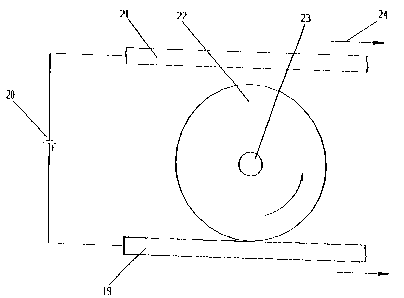
current is shown in Figure 2 for an etching process.
The material-for treatment 19 to be etched is connected
via electrically contacting clamps not shown to the
positive pole of the source of bath current 20. The
other pole of the source of bath current is connected
to a cathode 21. A roller 22 longitudinally extended
to the plane of the drawing as an intermediate
electrode is highly electrically conductive at least on
its surface. It is mounted to be vertically adjustable
with its bearing pins 23, so that different thicknesses
of printed circuit boards are automatically compensated
for. A very small spacing between the surface of the
~
219133915
material for treatment and the roller-shaped
intermediate electrode is enabled and kept constant by
insulating and preferably extremely thin spacer means,
which are not shown here. The roller rotates at a
speed of rotation which preferably corresponds to the
transport speed of the material for treatment in a
horizontal. direction. If differing speeds are
selected, the surface of the intermediate electrode
wipes along the surface of the material for treatment.
I0
The spacing between the counter-electrode 2i polarised
as a cathode and the roller is not critical as regards
the quality of electrolytic processing of the material
for treatment. By means of sporadic offsetting of the
i5 cathode in the direction of arrow 24, the point at
which the largest quantity of metal etched off the
material for treatment deposits and is located in the
effective area of the roller, can be displaced
laterally, so that a new surface area of the cathode,
20 upon Which no metal or only a small amount of metal has
as yet deposited, is moved into the named area. In
this way the available cathode surface for depositing
of etched off metal is totally usable.
25 An advantage in this respect is that, in the etching
process described, a recovery of metal takes place_
Additional chemical recovery methods are therefore not
necessary. During electrolytic etching the metal
passes from the material for treatment firstly on to
i 219133916
the roller and then on to the cathode. For this
purpose according to the invention only one source of
bath current is necessary. Furthermore, no electrical
contacting of the roller is necessary. In an etching
installation, a plurality of rollers are preferably
disposed in the transport direction of the material for
treatment in succession. Similarly, these may also be
located for two-sided and/or synchronous treatment of
the printed circuit boards, on the underside of the
to same.
Figure 3 shows a theoretical view for metallisation of
printed circuit boards 25 in a horizontal position.
The source of bath current 26 is connected to the
positive pole at the counter-electrode (anode) 27 lying
opposite the material for treatment 25, the negative
pole to the material for treatment 25. The rotating
roller 22, as already described with reference to
Figure 2, is in the form of an intermediate electrode.
The anode 27 may be in the form either of an insoluble
or as a soluble electrode. In both cases an extremely
small constant spacing is set between the material for
treatment and the intermediate electrode.
Independently of this, the path between the aaode and
the roller is not critical for the quality of the
deposited metal coating on the material for treatment
This pernv.ts the use of cost-effective soluble anodes,
whose geometry due to the permanent dissolution cannot
be kept constant, and therefore would be unsuitable for
2191339
direct use without the intermediate electrode according
to the invention and with a very small spacing between
anode and cathode.
By means of sporadic offsetting of the soluble anodes
in the transport direction 24, in this case also all
areas of the anode in succession are used for
metallising. The area on the anode Iying opposite the
upper contour line of the roller is continuously most
intensely etched. By means of offsetting in direction
24, areas of the anode from which no metal or only a
little metal has yet been etched, is brought into a
positioa lying opposite the named contour line of the
roller. Far electrolytic metallisation of both sides of
the printed circuit boards, corresponding devices with
roller-shaped intermediate electrodes are also located
on their undersides.
The invention is not restricted to the use of roller-
shaped intermediate electrodes, but also includes such
electrodes of a different shape with an if necessary
relative movement equivalent to rotation to the other
elements of the cell which are available for
interaction.