Language selection

Search

Patent 2191807 Summary

Third-party information liability

Some of the information on this Web page has been provided by external sources. The Government of Canada is not responsible for the accuracy, reliability or currency of the information supplied by external sources. Users wishing to rely upon this information should consult directly with the source of the information. Content provided by external sources is not subject to official languages, privacy and accessibility requirements.

Claims and Abstract availability

Any discrepancies in the text and image of the Claims and Abstract are due to differing posting times. Text of the Claims and Abstract are posted:

  • At the time the application is open to public inspection;
  • At the time of issue of the patent (grant).
(12) Patent: (11) CA 2191807
(54) English Title: CIRCUIT ARRANGEMENT HAVING A PLURALITY OF CIRCUIT UNITS AND A COMMON MULTI-WIRE CABLE
(54) French Title: CIRCUIT COMPORTANT PLUSIEURS SOUS-CIRCUITS ET AYANT UN CABLE MULTI-FILS EN COMMUN
Status: Expired and beyond the Period of Reversal
Bibliographic Data
(51) International Patent Classification (IPC):
  • H05K 03/36 (2006.01)
  • H01R 13/66 (2006.01)
  • H05K 03/34 (2006.01)
(72) Inventors :
  • ELSINGER, HERBERT (Germany)
  • OBERNDORFER, JOHANNES (Germany)
  • PLAPPERT, FRIEDRICH (Germany)
  • TAJIMA, SHIGERU (Japan)
(73) Owners :
  • EURO-MATSUSHITA ELECTRIC WORKS AKTIENGESELLSCHAFT
(71) Applicants :
  • EURO-MATSUSHITA ELECTRIC WORKS AKTIENGESELLSCHAFT (Germany)
(74) Agent: KIRBY EADES GALE BAKER
(74) Associate agent:
(45) Issued: 2000-08-15
(22) Filed Date: 1996-12-02
(41) Open to Public Inspection: 1997-06-15
Examination requested: 1997-02-24
Availability of licence: N/A
Dedicated to the Public: N/A
(25) Language of filing: English

Patent Cooperation Treaty (PCT): No

(30) Application Priority Data:
Application No. Country/Territory Date
195 46 782.5 (Germany) 1995-12-14

Abstracts

English Abstract


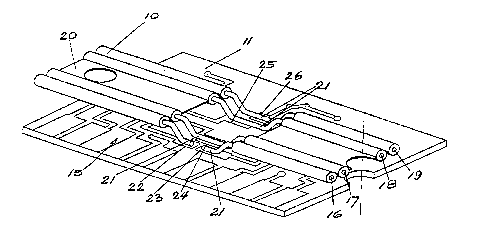
In an electrical circuit arrangement, specifically a se-
quential blasting system as used in mining, the individual
circuit units 12 are contacted by a continuous flat cable 10
in such a way that each wire 16 to 19 of the cable 10 has a
bared section 21 which is soldered to a contact pad 22 to 26
of a conductor pattern 15 disposed on a printed circuit board
11 which carries the circuit elements of the circuit unit 12
This not only minimises the total number of contacts but also
prevents the contact points from increasing the line resis-
tance and prevents any faulty contact point from interrupting
the line.


French Abstract

ans un agencement de circuit électrique, précisément un système de tir séquentiel comme ceux utilisés en abattage à l'explosif, les cartes d'équipement de circuit 12 sont reliées à un câble plat continu 10 de telle façon que chaque conducteur 16 à 19 du câble a une section dénudée 21 qui est soudée à un plot de contact 22 à 26 d'une impression conductrice 15 disposée sur une plaquette de circuits imprimés 11 qui porte les éléments de circuit de la carte d'équipement de circuit 12. Ceci non seulement minimise le nombre total de contacts, mais aussi empêche les doigts de contact d'augmenter la résistance de ligne et empêche la coupure de la ligne par un doigt de contact défectueux.

Claims

Note: Claims are shown in the official language in which they were submitted.


- 7 -
Claims
1. An electrical circuit arrangement comprising
a plurality of circuit units each including a conductor
pattern formed on a printed circuit board, and
a multi-wire cable interconnecting all said circuit
units and including a plurality of wires, each wire having a
portion exposed within the area of each circuit unit and con-
nected to a portion of the respective conductor pattern, at
least one of said wires being uninterrupted and connecting
all circuit units in parallel.
2. The circuit arrangement of claim 1, wherein each wire
has a bare intermediate section directly contacting a portion
of the respective conductor pattern.
3. The circuit arrangement of claim 2, wherein one of the
wires is interrupted at said bare intermediate section with
both ends thus formed contacting separate portions of said
conductor pattern.
4. The circuit arrangement of claim 1, including contact
elements mounted on said printed circuit board, each contact
element having a first end connected to said conductor pat-
tern and a second end forming a knife-edged terminal for
penetrating an insulation of said multi-wire cable to contact
a respective wire thereof.
5. The circuit arrangement of claim 4, wherein all contact
elements disposed on the same printed circuit board are stag-
gered along the direction of said cable.
6. The circuit arrangement of claim 1, wherein said circuit
units constitute trigger stages of a sequential blasting sys-
tem and said multi-wire cable is formed as a flat cable.

Description

Note: Descriptions are shown in the official language in which they were submitted.


2191807
-- 2 --
Background of the Invention
In mi n; ngr blasting systems are used for se~uentially
triggering explosive charges placed in bore holes a~ a work-
ing face. Each explosive charge is ignited ~y an associated
5 trigge~ stage, and all trigger stages are connected in cas-
cade with a pulse source via a control line. The control line
often takes the form of a ~lat cable usually including four
wires; some circuits require only three or e~en only two
wires. Examples for ~uch sequen~ial blasting systems are
lo descri~ed in Canadian Patent Application No. 2,147,676 and
German Patent No. 4,433,880.
The circuit co~ponents of each trigger st~ge are usually
assembled on a printed circuit board enclosed in a protecti~e
casing. The circuit board is provided with contact points ~or
connecting, by ~oldering, the i nco~i ng control line, the out-
going control line, and branch lines which lead to one or
more explosive charges. This results in two soldering points
for each indi~idual wire of the control line within the area
of e~ch trigger stage, which not only necessitate~ corre-
sponding expenditure in manufacture but also in~olves a riskof faulty contacts.
In seq~ential blasting ~ystems, a single faulty co~t~ct
may result in only part of the explosive charges being trig-
gered or in explosions being simultaneously initiated at a
25 plurality of locations, depending on the ~ype of circuitry
employed and on the location of ~he fault. In any case, the
propag~tion of the explosion pressure wave, which has been
designed by suitably placing of the blasting system, is dis-
turbed and the e~ficiency o~ the ~equential blasting system
30 is a~ least substantially reduced. Moreover, an interruption
of the control line within the region o~ its connection to a
trigger stage may be caused by tensile stress exerted on the
control line, ~hich frequently occurs due to rough handling,
particularly in underground mining.

2191~07
.
-- 3 --
Summary of the In~ention
It is an o~jec~ o~ the invention to reduce the risk of
line interruptions or faulty contacts in an electrical cir-
cuit arrangemen~ which includes a plurality of circuit units
connected to a multi-wire cable.
To meet this object, the invention provides an electri-
cal circuit arrangement comprising a plurality o~ circuit
units each including a conductor pattern ~ormed on a printed
circuit board, and a ~ulti-wire cable inte~connecting all
these circuit units and including a plurality of wires, each
wire having a portion exposed within the area of each circuit
unit and connected to a portion of the respecti~e conductor
pattern, at least one of the wires being uninterrupted and
connecting all circuit units in parallel.
Those wireS ~f the ~uLti-wire cable which serve for the
common supply of all units are continuous for all circuit
units. They are stripped of their insulation only over part
of their lengths wi~hin the region of contact with each cir-
o cuit unit If thiQ contact is faulty due to manufacture orbecomes interrupted, such as ~y excessive tensile forces act-
ing on the cable, it is only the respective circuit unit that
will fail, while the overall line r~m~ins uninterrupted. In
the case of a sequential blasting system with appropriately
designed electrical circuits, this means that only one single
explosive charge or a small number of them are not triggered,
whereas the o~erall blasting system can still fulfil its
function.
In an embodiment of the in~ention, each wire has a bare
20 intermediate section directly contacting a portion o~ the re-
spective conductor pattern. This results in a mi n; mllm total
number of contacts.
Wires which are not continuous for all circuit units re-
~uire only two solderi~g points. In known sequential blasting
systems, this regularly applies to only that one wire which
passes a trigger sisnal from one stage to the next.

2191807
According to another embodiment of the invention, con-
tact elements are ~ounted on the printed circui~ board, each
contact element having a ~irst end con~ected to the conductor
pattern and a second end forming a knife-edged term; n~ 1. for
s penetrati~g a~ insulation of the multi-wire cable to contact
a respecti~e one of the wires. This is advantageous with re-
spect to manuf~cture because it requires no specific step for
stripping the insulation from portions within the length of
the cable. Using thi~ type of contact element, it is pre-
lo ferred that all contact elements disposed on the same printedcircuit board a~e staggered along the direction of the cable,
to provide sufficient space ~or the contact elements even if
the wires of the cable axe arranged co~r~tively close to
each other.
Brie~ Description o~ the Drawings
Preferred embodiment~ o~ the in~ention will now be ex-
plained with reference to the drawings, in which
Figure 1 is a side view, partially in section, of a cir-
cuit unit contained within a protective casing
20and disposed along the le~gth o~ a control line
in the form of a flat cable,
Figure 2 is a schematic perspective view of the cable of
~igure 1 in the region where it contacts a
printed circuit board carrying the components
25of the circuit unit, and
Figures 3a to 3c are representations showing another em-
bodiment using contact elements pro~ided on a
printed circuit board ~or connection to the ca-
ble.
30D~tailed Description o~ P~eferred Fmho~3i m~nts
As shown in Figure 1, a junction, which is provided in a
flat cable 10 and constitu~e~ a trigger stage of a sequential
blasting system, is formed by an elec~rical circuit un-t 12
disposed on a printed circuit board 11 and enclosed in a pro-

21~1807
.~.
- 5 -
tective casing 13. In Figure 1, the various circuit compo-
nents, indicated at 14, o~ the circuit unit 12 are disposed
on the lower side o~ the printed circuit board 11 while a
conductor pattern 15 which interconnects the circuit compo-
5 nents is provided at the upper side of the board 11. In Fig-
ure 2, portions of the conductor pattern 15 are shown sche-
matically .
As illustrated in Figure 2, the flat cable 10 in the
present embodiment has ~our wires 16 ~o 19 com~o~ly embedded
lo in an insulating material which defines a centre web 20.
Within the region of the printed circuit board 11, all ~our
wires 16 to 19 are stripped of their insulation The bare
sections 21 of the wires are multiply bent to form wire sec-
tions which extend parallel to the ~lat cable 10 but are o~f-
15 set downwa~d therefrom. As shown in Figure 2, these sections21 are soldered to contact pads 22 to 26 of the conductor
pattern 15.
While the wires 17 to 19 are continuous and connected at
their bare sections 21 to respective ones o~ the contact pads
20 24 ~o 26, the wire 16 is interrupted in its bare inter~ediate
section 21, and the two ends thus formed are soldered to
separate contact pads 22, 23 of the conductor pattern 15.
In a particularly economic manufacturing method, the
wire sections 21 are soldered to the contact pads 22 to 26 in
the same step in which the circuit co~ponents 14 are soldered
to the conductor pattern lS (provided on the lower side of
the printed circUit board 11 and not visible in Figure 2).
As illustrated in Figure 2, the conductor wires 17 to 19
are uninterrupted also in the region where they are connec~ed
30 to the circuit units 12 p~ovided o~ the printed circuit ~oard
11 so that any faulty contaCt that may exist does not cause
an interruption of the wire. For ~he same reason, the solder-
ing points do not increase the line resista~ce.
In a second embodiment of the in~ention show~ in Figure
3~ 3, the flat cable 30 is so formed ~hat the insulation forms
web 40 between each pair of adjacent wires 36 to 39. Further,

2191807
._
-- 6 --
the indi~idual wires 36 to 39 have ~o section of the insula-
tion stripped off but are inserted in knife-edged terminals
41 which in turn are inserted in the printed circuit board 31
and soldered to the csn~lctor pattern 35 (not shown in de-
5 tail) which in this case is provided on the lower side of theboard 31.
In Figure 3, (a) shows the condition prior to the cable
30 contacting the knife-edged ter~;~a~s 41, while (b) shows
the condition after contacting. (c) is a plan view of the ar-
rangement shown at (b).
As is apparent from Figures 3(a~ and (b), the ~ni~e-
edged ter~;n~l ~ 41 are fork-shaped with two upwardly pointed
tines 42. The mutually facing edges of the ~ines 42 are
kni~e-shaped ~nd together form a slot 43 havi~g a width
15 slightly ~maller than the diameter of the wires 36 to 39. The
tines 42 of each fork are inwardly cha~fered so as to pene-
trate the webs 40 of the flat ca~le 30 between adjacen~ wires
and lead the respective wire into the slot 43.
Accordi~g to Figure 3(c), the t~m' n~l s 41 are staggered
in ~he longit~in~l direction of the f}at cable 30 to avoid
mutual contact between termi n~l s ~1 without requiring exces-
sively wide webs 40 in the cable 30.
Figure 3(c) further shows an example in which, similar
to Figure 2, one of the wires, 36, ls interrupted wlthin the
region of the junction, and either one of the two ends thus
formed is contacted by its own knife-edged ter~in~ 41.
Compared to the arrangement o~ Figure 2, the embodi~ent
of the invention shown in ~igure 3 has a manuf acturing ad~an-
tage in that it requires neither removing the insulation from
30 any sections of the flat cable nor bending of the bared wire
sec~ions. On the o~her hand, the embodiment of Figure 2 has
the ad~antage ~hat it requireC no additlonal contact elements
(knife-edged term; n~l s) and one single soldering connectlon
contacts the wire directly with the corresponding portion of
35 the conductor pattern.

Representative Drawing
A single figure which represents the drawing illustrating the invention.
Administrative Status

2024-08-01:As part of the Next Generation Patents (NGP) transition, the Canadian Patents Database (CPD) now contains a more detailed Event History, which replicates the Event Log of our new back-office solution.

Please note that "Inactive:" events refers to events no longer in use in our new back-office solution.

For a clearer understanding of the status of the application/patent presented on this page, the site Disclaimer , as well as the definitions for Patent , Event History , Maintenance Fee  and Payment History  should be consulted.

Event History

Description Date
Inactive: IPC deactivated 2011-07-29
Inactive: IPC from MCD 2006-03-12
Inactive: First IPC derived 2006-03-12
Inactive: IPC from MCD 2006-03-12
Time Limit for Reversal Expired 2001-12-03
Letter Sent 2000-12-04
Grant by Issuance 2000-08-15
Inactive: Cover page published 2000-08-14
Inactive: Final fee received 2000-05-15
Pre-grant 2000-05-15
Letter Sent 1999-11-24
Notice of Allowance is Issued 1999-11-24
Inactive: Approved for allowance (AFA) 1999-10-27
Inactive: Application prosecuted on TS as of Log entry date 1998-04-21
Inactive: Status info is complete as of Log entry date 1998-04-21
Inactive: Adhoc Request Documented 1998-04-21
Letter Sent 1997-12-22
Application Published (Open to Public Inspection) 1997-06-15
All Requirements for Examination Determined Compliant 1997-02-24
Request for Examination Requirements Determined Compliant 1997-02-24
All Requirements for Examination Determined Compliant 1997-02-24

Abandonment History

There is no abandonment history.

Maintenance Fee

The last payment was received on 1999-10-06

Note : If the full payment has not been received on or before the date indicated, a further fee may be required which may be one of the following

  • the reinstatement fee;
  • the late payment fee; or
  • additional fee to reverse deemed expiry.

Patent fees are adjusted on the 1st of January every year. The amounts above are the current amounts if received by December 31 of the current year.
Please refer to the CIPO Patent Fees web page to see all current fee amounts.

Fee History

Fee Type Anniversary Year Due Date Paid Date
Registration of a document 1996-12-02
Request for examination - standard 1997-02-24
MF (application, 2nd anniv.) - standard 02 1998-12-02 1998-10-21
MF (application, 3rd anniv.) - standard 03 1999-12-02 1999-10-06
Final fee - standard 2000-05-15
Owners on Record

Note: Records showing the ownership history in alphabetical order.

Current Owners on Record
EURO-MATSUSHITA ELECTRIC WORKS AKTIENGESELLSCHAFT
Past Owners on Record
FRIEDRICH PLAPPERT
HERBERT ELSINGER
JOHANNES OBERNDORFER
SHIGERU TAJIMA
Past Owners that do not appear in the "Owners on Record" listing will appear in other documentation within the application.
Documents

To view selected files, please enter reCAPTCHA code :


To view images, click a link in the Document Description column. To download the documents, select one or more checkboxes in the first column and then click the "Download Selected in PDF format (Zip Archive)" or the "Download Selected as Single PDF" button.

List of published and non-published patent-specific documents on the CPD .

If you have any difficulty accessing content, you can call the Client Service Centre at 1-866-997-1936 or send them an e-mail at CIPO Client Service Centre.


Document
Description 
Date
(yyyy-mm-dd) 
Number of pages   Size of Image (KB) 
Representative drawing 1997-08-25 1 22
Representative drawing 2000-08-08 1 16
Description 1997-05-04 5 244
Abstract 1997-05-04 1 19
Claims 1997-05-04 1 39
Drawings 1997-05-04 2 62
Acknowledgement of Request for Examination 1997-12-21 1 178
Reminder of maintenance fee due 1998-08-04 1 115
Commissioner's Notice - Application Found Allowable 1999-11-23 1 164
Maintenance Fee Notice 2001-01-01 1 178
Correspondence 2000-05-14 1 40
Correspondence 1997-01-06 1 38