Note: Descriptions are shown in the official language in which they were submitted.
219223~
- ELECTROMAGNETIC SENSITIVE SWITCH
Field of The Inve-ntion
The Present relates to a keyswitch, more ParticularlY~
to an electromagnetic sensiti-ve switch suitable used on
keYboard.
To the historY of the keYboard for computer, the
earliest-one is mechanic On-Off tYpe, then a true-N-key is
introduced, which belongs to depress-and-output tYpe. Regarding
to the matrix of the keYboard, a short N keY is used.
The keYboard is used to inPUt information, there shall
not anY missing word, including sYmbol. On the other hand, when
the information is inPut in a quite high sPeed, there shall not
any incorrect words. On the other hand, an excellent keyboard
must be inherited with linear, without break Poin~ and noiseless.
Ln the prior art, there are a Plurality of keyboard
which has a b-reak point, noise as well as non-linear. These can
not be referred to as an excellent keYboard. In some keyboard,
an diode is added into the matrix to establish an improvement
to the ture-N-keY. In this kind of keYboard, it is contrPlled
and adjusted bY the IC chiP, On-Off adiust circuit, and latching
control. Then it maY has an excellent caPabilitY of few mistake.
Nevertheless, each keYswitch shall be incorPorated with an diode,
accordingly, there are 108 ndiodes shall be aPPlied since there
are 108 keYswitch ina standard keyboard. In light of this, not
only will the cost increase tremendously, but will also bring
difficulty during the manufacturing. By the way, it can not be
2192230
~ adaPted to~menbrane switches or plastic membrane.
In the Past, there is a caPacitor-tYPe keYswitch which
includes an uPper conducting laYer, a contacting laYer and a
lower conducting layer. Nevertheless, the manufacturing cost
is high and the service life is short. Furthermore, it can be
readilY influenced bY the moisture, consequentlY, it has a Poor
stabilitY. AccordinglY, the keYswitch of caPaacitor tYpe has
been phased out because of its cost and Poor function.
In the second tYPe of keyswitch, it is an
electromagnetic tYpe which includes the PCB, iron core winding
and amPlifYing winding. A through hole is disPosed in the
middle Portion. This kind of keYswitch need a double side- PCB
and with manY a windi~ngs thereof. On the other hand, the large
caPaeitance of caP-acitor means a high- cost. Accordingly,
it has been phased out as well.
Right now, a three layers conductin-g me-mbrane has been
apPlied for keYswitch, IBM's keYswitch is a tYPical one. In
this design, the virtual N-keY is constructed and controlled
by IC chip and controller. Nevertheless, it uses second auto
scanning to correct the missing and incorrect words. But it
still has a high manufacturing cost both on manufacturing and
material.
SummarY of the Invention
It is the obiect of this invention to Provide an
electromagnetic sensitive keyswitch wherein the dePressing
force exerted to each keyswtich can be readily adjusted to
- 2 -
219223~3 1
-lmprove t~he missing and incorrect input,
I't is still the obiect of this invention wherein the
make Point a-nd break point and the control to the circuit and
mechanism have been modified to provide a more reliable inPut.
It is still the object of t-his invention wherein the
On-Off status can be readily adjusted bY the,circuit and
controller. Accordingly, an excellent keYboard is attained.
It is still the object of t'his invention wherein the
upper and lower limits can be readily defined to establish the
On and Off status.
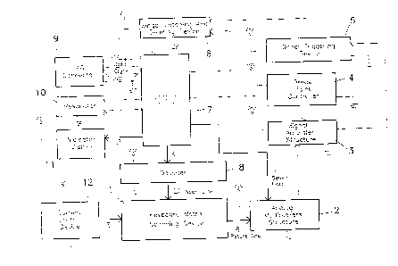
-As shown in Figure 1. the electromagnetic sensitive
switch comPrises a keyboard matrix scanning device 1, a analog
multiPlexer device 2. a signal amPlifier 3, a signal
triggering device 5, a break Point controller 4 during the
oPeration, a signal latching and deleting dev-ice 6, a CPU 7,
a decoder 8. an I/O connector 9, a resonator 10, an indicator
display 11 and a current control device 12.
The operating PrinciPle of the electromagnetic
sensitive switch is based on the following procedures.
SteP 1. the scanning of the key matrix is Performed bY
the scanning device, and a pluralitY of the keYs are scanned,
not onlY a signle one;
Step 2, the scan is performed bY the I/O connector;
Step 3, feedback and read in. multi-exhange
transmission is performed bY the multi-plexer 4051;
SteP 4, The OPA, current loop and voltage loop are
21g~23~ '
added for signal amPlification and sensibilit-Y enhancement;
SteP 5, signal adiustment is perfo'rmed to determine
the On-Off uPPer-lower limits for signal retrieving;
SteP 6, the break Point controller can be adiusted,
then bY the YR rheostat, the Pressing amPlitude o~f the on-off
switch can be adjusted. The structure of this key will be
specially designed. BY m~eans of this adiustment, a tailored
amount can be a'ttained for a certain user; - -
Step 7, the signal triggered by keYboard is Processed
by the CPU;
Step 8, the feedback is used to delete the signalthrough the resonator. The transient status of the keyboard is
deleted; and
Step 9, the latch deYice is used to prevent surge wave,
latching signal and dele~ting signal.
The electromagnetic sensitive switch can be concluded
with the following features.
1. The conducting membrane has " multi-laYer "
configuration wherein the uPper conducting layer, the
contacting layer and the lower conduction layer are all
manufac~ured into a merbrane. In the middle portion, each of
the keYswitch is incorPorated with a cross-linked two laYers
of metal layer. When the keYswitch is depressed, the amPere's
law will be aPPlied wherein the current takes 1~2 and the
magnetic field takes 1/2. The CPU and scanning matrix will
- ' select i-t.
2192~3~
~~ 2-. The correct character and symbol will be accurately
selected bY the CP-U and Pertinent software;
3. D-uring the scann-ing process, the scanning device
will read out al'l the dePressèd keYswitches simultaneously,
not o-ne by one.
4. The keYswitch is featured with a DeBounce
multi-rings caP. The keYswitch includes an uPPer and a lower
- conducting layers spaced apart from each other--by an
insulating laYer.
5. In the design, it includes a sPring, a lower
housing enclosed with winding. -The middle Portion is a
conducting membrane which has-an uPPer and lower metal layers.
The amPe-re's la-w is aPPlied in this case. The conducting
membrane is disPosed on the sPring, as shown in Figure 3-1 and
the sPring is porvided with a magnetic sensitive section formed
bY carbon powder.
The feature shown in Figure 1 is further illustrated
by Figure 2 which shows the circuitrY configuration. The
signal Processing and described in more details as follows.
The signal is a current signal from the keY matrix. It
passes 4051 IC and " oPerating amplifier ". The signal is
amPlified and formed into an upper Peak and lower valley and
then is adiusted by the varied rheostat. As it passes Scmffer
trigging device, the lower limit is set at 0.84 volts and the
upPer iimit is set at 1.7 volts.
219~23~
~ The present invention has ~he following advantage
1. There is no missing word;
2. It is line-ar and with excellent tactile'feeling;
3. The uPPer and lower limit of the On-Off states of
the keyboard can be readilY adJusted;
4. No no-ise;
5. No loss of fidelity,-;
- 6. High working speed; and
7. With design character,istics different from the
Prior art.
Brief DescriPtion of the Drawin~s
In order that the present invention may more readily
be understood the following description is given. esPeciallY
by way of examPle with reference to the accompanying drawings,
in which
Figure 1 is a sYstem block diagram of the
electromagnetic sensitive switch made according to this
invention;
Figure 2 is a sYstem block diagram of the function of
the Potential-control made according to this invention;
' Figu-re 3-1 and 3-2 are the cross sectional view of the
switch and the sYstem block diagram of the uP and down of the
keyboard;
Figure 4 is a toP view of the conducting membrane
keyboard of signle laYer; and
Figure 5 is a sketch view of the keYtoP of a conducting
2192230
membrane keYboard of single laYer.
Figure 1 includes keYboard matrix scanning device 1.
analog mu~tiplexer device 2, signal amPlifier 3, break Point
controller 4 during the oPeration, signal triggering device 5,
~5 signal latching and deleting device 6, CPU 7. decoder 8, I/O
connector 9, resonator 10, indicator disPlaY 11 and current
contro~ device 12.
-Figu-re 2 includes 4051 multiplexer 20, oPerating
amPlifier 22, rheostat 23, schmitter triggering device 24.
10Figure 3 includes a Plastic sheet 30, spring 31,
magnetic core 32 an-d resistance R.
Figure ~ includes an upper conducting membrane 3-3,
keYswitch 34 and lower conducting membrane 35.
Figure 5 includes a plastic sheet 30. sPring 31. coil
1536, carbon Powder 37. Plunger 3~ and magnetic detecting
portion 3g.
~etailed ~escri~tion of Preferred ~mbodiment
~ n the sYstem block diagram of the electromagnetic
sensitive switch. the keyswitches are selected bY the
aPPlication of the amPere~s law. The signal is selected,
enhanced and amPlified by the multiP~exer. Then the signal
Passes th signal triggering device to imProve the accuracY of
th uPPer and lower limit Potential, then the Hi-Low can be
readilY determined. Then the signal is Passed to the break
Point controller adiusting On-Off device which is a brand new
microProcessor control and does not aPPear ;n disclose bY the
-' 2192230
_ prior art. Then the signal is passed to signal feedback device
to imProve the stabilitY. Then the signal is passed to the
signal 1atching delete device which is attained by dual-nand
gate circuit. T-hen the signal is retrieved f-rom the signal
latching delete device and is s-ent to CPU by the software and
controller. BY this arrangement, the a stable signal can be
attained for the indicator disPlay.
The arrangement of the present invention Provides a
novel imProVement to the configuration of the keYswti~h and
the circuit. for example, the base gate is pro-vided at the
scanning portion and the stable Power suPPly is given for a
stable inPut scanning.
As shown in Figure 2. the adjusting circuit is Provided
to suit the accuracY of the mechanic structure to improve and
adiust the Potential.
As shown in Figure 3-2, an accurate elements are
provided. In Figure 3-2. the sPring is disPosed centrally to
be inserted into the central single laYer o-f the conducting
laYer. The single laYer of the keYswitch is formed by the upPer
and lower conducting membranes. The winding of the keyswitch is
disPose.d at the edge of the housing. The area beneath the
centrallY disPosed spring is Provided with carbon powder to
change the magetic effect in the middle portion. From ampere's
law. the conducting membrane maY generate a cross-linked
magnetic field may also generate a current resulted from
interacting. Not onlY does the feature of the Present invention
219223~
- locates on the electronic, mechanic, the sYstem Portion, s-ignal
laYer conducting membrane and keyswitch, but will also include
the circuit which construct the cross-linked uPPer and-l-ower
laYers and the current generated from the conducting membrane.
Those techniques have not been disclosed by the conventional art.
US Pat. 4'494'109 and 4'529'967 disclose the selection
of the keYboard by inductio~ and caPacitance resPectively.
Nevertheless, it has a poor f-unction, many a missing or
mistYPing have been encountered. On the other hand, the
manufacturing cost is comParativelY high. By the provision of
the Present invention, the problems encountered bY those two
U.S. Patents have been solved since the On-Off can be readily
adjusted to meet differènt requirements from different users.
In US-Pat. 4'494'109, it uses the non-contact tYpe and
utilize the transformer and secon-darY induction tYPe arra~
signal which Passes a multiplexer and a binarY/decimal converter
and binarY counter and storing latching circuit. This is
completely different with the Present invention, US Pat.
4'529'967 utilizes the sensitive shaPe and mutual induction
PrinciPle via base gate oPen circuit and decoder, analog
multiplexer and voltage comParator, inventor and microProcessor
to handle the assembled N-keY cycle. The keyswitch utilizes the
electromagnetic operation and incorporating the scan control.
This is also different with the Present invention.
US Pat. 3'B98'531 is a solid state of a keyboard which
uses alternative vibration and spring. In different magnetic
'" 219223~
- sectors, it generates different cross-linked current wave and
detected by Potential level later. Then a Pulse is generated
and gate control S~. The signal is sent to outPut gate. The
configuration and working principle are different with the
present invention.
US Pat. 3'740'746 uses inductive magnetic/drum, two
half/-circle edge and insulating Plate-to construct the matrix
coding transformation. It has at least for three layers of uPper
insulating laYer, the upper and lower magnetic sectors. The
structure, shaPe and couPling are from the present invention.
US Pat. 4'283'71~ discloses cross matrix sensitive
keyboard which ls different with the Present invention.
US Pat. 3'641'567 discloses a non-contacting inner-
locking system which utilizes the middle cross-linked channels
and magnetic ring incorPorated with multi-plexer and comParator.
This is diff-erent with the Present invention.
US Pat. 4'300'127 discloses a solid state non-
contacting stYle. It takes two cross-linked magnetic rings with
a matching magnetic core. The oPerating current of the keyswitch
is generated bY PrimarY nickel coil winding.
' US Pat. 4'344'068 discloses a magnetic ring magnetic
sPring collecting system. It takes magnetic block and different
magnetic sectors incorporated with matrix to scan the signal.
Then the signal Passes an amplifier, a comParator, a shift
register and latching and microporcessor. On the other hand,
the voltage and current can be increased by the differential
- 10 -
' 219223G
amPlifier and line current or voltage. This is also different
with Present invention.
While Particular embodiment of the Present invention
has been illustrated and described for keyboard, it would be
obvious to those skilled in the art that various other changes
and modifications can be made without departing from the sPirit
and scoPe of the invention. It is therefore intended to cover
in the aPPended claims all such changes and modifications that
are within the scoPe of the Present invention.