Note: Descriptions are shown in the official language in which they were submitted.
219230
WO 95/34003 PCT/US95/06885
LOW POWER MAGNETOMETER CIRCUITS
BACKGROUND OF THE INVENTION
Field of the Invention
This invention relates to devices and circuitry
for measuring magnetic fields and more particularly to
magnetometer circuits for measuring magnetic fields.
Descrit~tion of Related Art
A number of different types of magnetometers are
available. However, of the various types presently
available, a fluxgate magnetometer is one of the more
practical types for the measurement of weak static
magnetic fields. Fluxgate magnetometers rely on the
saturation of a magnetic core to provide a basis to
measure an absolute magnetic field. The current
required to bring the core into saturation is the major
source of power consumption for the magnetometer.
While it is possible to reduce the power consumption of
traditional fluxgate magnetometer sensing techniques
for low power applications by reducing the sampling or
measurement time, these adaptations do pose a few
significant design challenges. With the more reliable
second-harmonic fluxgate detection scheme, it is not
easy to simply reduce the number of excitation waveform
cycles; most systems involve some degree of filtering,
which requires many excitation cycles to settle. While
it is easier to adapt a peak detection scheme to use
only a few excitation cycles, as found in U.S. Patent
4,668,100, issued May 26, 1987 to Murakami et al., peak
detection fluxgate systems generally have inferior
accuracy. In Murakami et al., a toroidal coil is
utilized. It is much more straightforward to adapt a
frequency-mode magnetometer detection scheme such as
that found in U.S. Patent 5,239,264, issued August 24,
-1-
WO 95/34003 219 2 3 3 ~ PCT/US95/06885
1993 to Timothy J. Hawks. In the Hawks patent, a
solenoidal coil is used instead of the Permalloy
toroidal coil described in the Murakami et al. patent.
Using a simple L/R relaxation oscillator with the
solenoidal coil, the magnetometer circuit has an almost
instantaneous start-up time. As a direct consequence,
it is quite simple to gate the oscillator on for short
periods of time while retaining the ability to acquire
a period of the waveform to measure the magnetic field
value. This circuit still suffers from the requirement
for a significant peak current to drive the sensor
coil.
An earlier additional magnetometer is disclosed in
U.S. Patent 4,851,775 issued July 25, 1989 to Kim et
al. In the Kim et al. patent a solenoidal sensor coil
is utilized. However, the magnetometer of Kim et al.
suffers from the same disadvantages as U.S. Patent
5,239,264 for low power applications.
There is a need to reduce the overall power
consumption in magnetometers over that which has been
available in prior art magnetometers. One of the
objects of the present invention is to reduce the
amount of power required to measure the magnetic field.
SUMMARY OF THE INVENTION
In accordance with the present invention a
magnetometer circuit is provided which, in one
embodiment, a sensor coil including a saturable core is
provided a source potential to bring the coil toward a
saturation point, followed by a deactivation of the
potential to the coil. The current through the coil is
sensed and the magnetic field affecting the coil may be
determined based on the amount of time that is required
for the current to the coil to decrease from a first
predetermined amount to a second predetermined amount.
The current sensor provides a first output signal in
-2-
77672-1 CA 02192330 2000-02-16
3
response to the current through the sensor coil increasing to a
first threshold level in a first portion of the cycle, and
provides a second output signal in response to the current
through the sensor coil decreasing to a second threshold level.
The time period between these first and second output signals
is indicative of the magnitude of the field affecting the coil.
In accordance with another embodiment of the present
invention, a magnetometer circuit is provided in which zero
cancellation is achieved. In one embodiment of the zero
cancellation circuit, a first and a second state of operation
are provided. In the first state of operation a first terminal
of the sensor coil is alternately connected to a first source
of potential and then a second source of potential and a
current sensor is connected to the second terminal of the coil
to measure the current through the coil. In the second state
of operation, the second terminal of the coil is alternately
connected to the first source potential and then the second
source of potential and the current sensor is connected to the
first terminal of the coil to measure the current flow through
the sensor coil.
The invention may be summarized, according to a first
broad aspect, as a magnetometer circuit capable of measuring a
magnetic field during one switching cycle, said magnetometer
circuit comprising: a sensor coil including a saturable core,
said sensor coil having first and second terminals; a first
impedance having first and second terminals; means connecting
said first terminal of said first impedance to said second
terminal of said sensor coil and means connecting said second
terminal of said first impedance to a ground potential; a first
switch for selectively connecting said first sensor coil
terminal to a voltage node for receiving a voltage provided by
a voltage source during a first portion of said one cycle; a
77672-1 CA 02192330 2000-02-16
3a
second switch for selectively connecting said first sensor coil
terminal to said ground potential during a second portion of
said one cycle; a voltage sensor having an input terminal and
an output terminal, said voltage sensor providing at said
output terminal thereof an output signal of a first magnitude
in response to a voltage at said input terminal thereof
exceeding a first threshold, and said voltage sensor providing
at said output terminal thereof an output signal of a second
magnitude in response to said voltage at said input terminal
thereof falling below a second threshold; means connecting said
input terminal of said voltage sensor to said second terminal
of said sensor coil; a control circuit having first and second
input terminals for receiving input control signals and first
and second output terminals for providing control signals;
means connecting said output terminal of said voltage sensor to
said first input terminal of said control circuit; means
connecting said first output terminal of said control circuit
to said first switch to control operation of said first switch;
and means connecting said second output terminal of said
control circuit to said second switch to control operation of
said second switch.
According to a second broad aspect, the invention
provides a magnetometer circuit capable of measuring a magnetic
field during a single switching cycle, said magnetometer
circuit comprising: a sensor coil including a saturable core,
said sensor coil having first and second terminals; a first
switch for selectively connecting said first sensor coil
terminal to a power supply during a first portion of said
switching cycle; a second switch for selectively connecting
said first sensor coil terminal to ground potential during a
second portion of said switching cycle; a current sensor for
measuring current flow through said sensor coil, said current
77672-1 CA 02192330 2000-02-16
3b
sensor having an input terminal and an output terminal; means
coupling said input terminal of said current sensor to said
second terminal of said sensor coil to provide a path for
current flow through said sensor coil to ground potential and
to permit measurement by said current sensor of current flow
through said sensor coil; and circuitry for controlling said
first and second switches in said switching cycle such that
during said first portion of said switching cycle a connection
between said second terminal of said sensor coil and ground
potential is maintained through said current sensor and said
first switch connects said power supply to said first sensor
coil terminal, and during said second portion of said switching
cycle a connection between said second terminal of said sensor
coil and ground potential is maintained through said current
sensor and said second switch connects said first coil terminal
to ground potential, wherein said current sensor provides at
the output terminal of said current sensor a first output
signal in response to the current through the sensor coil
achieving a first threshold level, and said current sensor
provides at the output terminal of said current sensor a second
output signal in response to the current through the sensor
coil decreasing to a second threshold level.
BRIEF DESCRIPTION OF THE DRAWINGS
Other objects and advantages of the invention would
become apparent from a study of the specification and drawings
in which:
Figure la is a circuit diagram of a magnetometer
circuit according to one embodiment of the present invention;
77672-1 CA 02192330 2000-02-16
3c
Figure lb illustrates waveforms of the circuit of
Figure 1a, which are used in the explanation of the operation
of the circuit of la;
Figure 2 illustrates a magnetometer circuit
2192330
WO 95/34003 PCTIUS95/06885
,y.~r~
:~..~. a
,~
according to another embodiment of the present
invention;
Figure 3 illustrates additional waveforms useful
in connection with the description of the present
invention;
Figures 4a, 4b and 4c illustrate voltage sensor
circuits which may be utilized in the practice of the
present invention;
Figure 5 illustrates another embodiment of the
to present invention utilizing zero cancellation;
Figure 6 illustrates a further embodiment of the
present invention utilizing zero cancellation;
Figure 7 illustrates yet another embodiment of the
present invention utilizing zero cancellation;
Figure 8 is a circuit diagram of a magnetometer
circuit in accordance with the present invention, in
which two sensors are utilized to sense magnetic fields
in a first and a second axes; and
Figures 9a and 9b illustrate in block diagram form
two electronic compass systems utilizing magnetometer
circuits in accordance the present invention.
DETAILED DESCRIPTION OF THE INVENTION
As pointed out above, the current required to
saturate the core in a fluxgate magnetometer is a
significant source of power consumption. In accordance
with the present invention, the following two basic
strategies for reduction of the overall power
consumption resulting from saturating the core are
utilized: 1) reduction of the current required to
saturate the core, and 2) reduction of the amount of
time the core has to be saturated during measurement of
the field. The former strategy is achieved in two
different ways: first, by using magnetic core materials
that saturate at lower fields, and secondly, by
increasing the number of turns on the excitation coil.
-4-
219 2~3~3v
WO 95/34003 PCT/US95/06885
The present invention uses both of these techniques to
achieve a significant incremental improvement over
existing fluxgate technology. By using a thin
amorphous metal foil core instead of a Permalloy
toroid, the sensor requires a somewhat lower saturation
field. With a solenoidal geometry and a single
excitatiori/sense winding, it is economical to wind more
turns of wire on the sensor core than those on a
fluxgate excitation coil. The increased number of
windings helps to reduce the saturation current
requirement during excitation. Despite these
improvements, the most significant reduction in power
is achieved by the second strategy, the reduction of
core saturation time during measurement. The manner in
which the second strategy of power reduction is
achieved is described fully below.
The low power magnetometer in accordance with the
present invention not only overcomes the above-
described prior art problems while sampling for a brief
period, it also reduces the peak current required by
the sensor. The magnetometer requires only one
excitation cycle to sample the magnetic field.
Additionally, all the power needed by the sensor can be
supplied through a single capacitor, which reduces the
peak current requirements on the power supply to a
value closer to the average current.
Basic Sensor Theory
In order to understand the operation of the
magnetometer circuit in accordance with the present
invention, it is helpful to have simple model of the
sensor behavior. For example, in magnetometer circuit
1 in Figure la, sensor L is a solenoidal inductor with
a core 2 of saturable high-permeability material. A '
typical high permeability material suitable for the
core 2 is a cobalt-based amorphous metallic glass foil
-5-
2192330
WO 95/34003 PCT/US95/06885
r . a"''
~1',, ,~,r~,,
from Allied Signal, product number 2705M. A single
winding 3 is used not only to provide the excitation
signal but also to sense the changing field in the
core. The total magnetic field through the magnetic
core material is the sum of the external magnetic field
and the field created by current flowing through coil
3. The following equation describes this relationship:
H = koI + HE ( 1 )
where H is the total magnetic field through the core
material 2, HE is the external applied magnetic field
that is parallel to the core material 2, and I is the
current flowing through the inductor coil 3. Constant
ko is a function of the physical parameters of coil 3,
such as its turn density. When a high-permeability
material experiences a magnetic field, it effectively
amplifies this field by a large factor known as the
relative permeability. For many materials this factor
can be anywhere from 100 to 100,000 at the maximum
point. Typically, the permeability is high for only a
limited range of small fields. As the field applied to
the material is increased in either direction, the
permeability of the material drops off to a factor of
one. This reflects the saturating characteristic of
these materials. The relative permeability, as a
function of the applied field, is denoted as ~c(H). The
voltage across the sensor coil will be a function of
the change in the resulting magnetic field from the
material. This can be expressed as follows:
V-lcl~ (H) a (2)
where V is the voltage across the sensor coil, ~c(H) is
-6-
WO 95/34003 219 ~ ~ ~ ~ PCT/US95/06885
relative permeability of the core, and dH/dt is the
time derivative of the applied field. The constant k~ is
a function of several sensor physical parameters, such
as the turn density of the coil and the volume of the
coil material. When the external field HE is constant
(i.e. varies slowly with time), equations (1) and (2)
can be combined to produce the following:
V k°kl~ (H) dt (
As with a normal inductor, the voltage is related to
the time derivative of the current and can
alternatively be expressed as follows:
V=L(H) at (4)
where L(H) is defined accordingly:
L (H) =kokl~t (H) (5)
Note that the inductance is not constant but rather a
non-linear function of the magnetic field applied to
the material. Given this formalism of variable
inductance, it is possible to describe the output of
the magnetometer analytically as a function of the
applied field. The effects of material hysteresis are
not explicitly handled here. However, in the limiting
case of measuring a constant field over many identical
transitions, the relative permeability function does
tend to converge to a repeatable value, making the
above-mentioned relationships useful approximations.
WO 95/34003 219 2 3 3 0 PCT/US95/06885
The solenoidal design of~sensor L has a few key
advantages over its to~6lit5ial.'~'fluxgate counterpart. In
general, increasing the volume of windings (a function
of both the wire gauge and the number of turns) around
the sensor core reduces the sensor's power consumption;
if either the wire size or the number of turns is
increased, the power required to bring the sensor core
into saturation will be reduced. Additionally, the
number of turns used in the sense winding is
proportional to the output signal strength; increasing
the number of sense windings can reduce the required
amplification of the sensed signal. Solenoidal sensor
L has a single winding 3, thus excitation and sensing
are done with the same coil. For reduction of
excitation power, solenoidal sensor L can accommodate
more turns than an equivalent size fluxgate sensor, in
which the excitation windings must be threaded through
the toroid. Additionally, the increased number of
turns on solenoidal sensor L will enhance the output
signal strength. In many cases of prior art sensors,
the number of turns in the sense and excitation
windings must compete for the limited space around the
fluxgate sensor core.
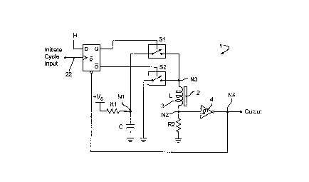
Magnetometer circuit 1 in Figure la illustrates
one embodiment of a magnetometer in accordance with the
present invention and provides a vehicle for explaining
the basis for the operation of the magnetometer
circuit. In the magnetometer circuit of Figure la, the
magnetometer output is not "zero-compensated"; that is,
the output for the magnetometer circuit with no
external field applied is, in practice, not repeatable
over temperature and component variation. Alternative
embodiments described later will correct this
deficiency. In magnetometer circuit 1, the output '
(illustrated in Figure lb) is a logic signal whose
pulse width t(HE) changes with the magnetic field
_g_
WO 95/34003 O PCT/US95/06885
applied to the sensor L. The current through sensor L
is converted to a voltage by resistor R2 and measured
by the inverting Schmitt Trigger 4. Referring to
Figure la, energy for saturation of sensor L is
provided by capacitor C, with the ground node providing
a first power terminal and node N1 (at the top of
capacitor C) providing a second power terminal. Node
N3 is a first terminal of sensor coil L, this terminal
being alternately connected between node N1 via switch
S1 and to ground via switch S2. To measure the current
flow through sensor L, a resistor R2 is connected
between the second terminal N2 of sensor coil L and
ground. The current sensor is completed by inverting
Schmitt Trigger 4 having its input connected to node N2
and its output connected to Node N4. A logic high
(indicated by H in Figure la) is continuously applied
to the D input of D flip-flop 5. To start a
measurement cycle, an Initiate Cycle signal
(illustrated in Figure lb) is applied to D flip-flop 5
via line 22. The D flip-flop 5 alternately activates
analog switches S1 and S2, as described in further
detail below. Capacitor C provides the energy to
saturate the sensor, and it is slowly charged through
resistor R1 from the positive power supply VS.
Alternatively, power to saturate sensor coil L could be
provided by connecting a power supply directly to node
N1.
The waveforms in Figure 1b show the process of
taking one measurement of the magnetic field HE. The
process is initiated by a rising edge of the Initiate
Cycle Signal which is applied to line 22 and sets the
flip-flop 5 such that S1 is closed. In this first
phase of operation, capacitor C, sensor L, and resistor
R2 form an under-damped RLC circuit in which the charge '
on C is dumped into the sensor inductor. As the
current through the sensor inductor increases, the
-g-
WO 95/34003 219 2 3 3 U
PCT/US95/06885
voltage across R2 increases until it reaches the
Schmitt Trigger's positive-going threshold voltage, VH.
At this point, the output of the Sghmitt Trigger goes
low and resets flip-flop 5. Stitch S1 is opened and
switch S2 is closed, connecting~node N3 of sensor L to
ground. During this second phase of the cycle, the
energy stored in sensor L is discharged through R2
until the voltage across resistor R2 reaches the
Schmitt Trigger's negative-going threshold, VL. The
output of the Schmitt Trigger then returns high,
completing the output pulse. The width of the pulse in
terms of the time from the falling to rising edges of
the output, indicated by t(HE) in Figure lb, will be
approximately proportional to the external magnetic
field HE applied to sensor L. If the inductance of
sensor L was linear, the output pulse width could be
calculated as follows:
_ v
t R2 1~ VLl
(6)
In this case the pulse width would be proportional to
the inductance of sensor L. However, due to the non-
linear inductance characteristic of the sensor L, the
pulse width needs to be calculated as follows:
t (HE) - 1 /'iN L (koI+H$)
R2 JzL I dI
(7)
where low and high threshold currents, IL and IH,
respectively, are defined accordingly:
-10-
7~
WO 95/34003 PCT/US95106885
IL= R2 . ( $ )
IH R2 (9)
The integral equation (7) shows how the inductance
function is convolved with a hyperbolic weighting
function, reflecting the fact that the sensor
inductance at the start of the discharge cycle
(near IH) contributes less to the overall output pulse
width than the inductance at the end of the discharge
(near IL) .
Figure 3 illustrates how the field H over time
relates to the variable sensor inductance. The
operating points in Figure 3 are shown for no external
field. The external field HE will change the operating
range on the inductance curve and thereby change the
period of the output. An external field HE which
magnetizes the sensor core in the same direction as the
excitation field (produced by application of a
potential to sensor L) will tend to decrease the
average inductance and thus the period of the output
pulse. On the inductance curve of Figure 3, this would
shift the operating points towards the right. An
external field which opposes the excitation field will
conversely increase the inductance and the output pulse
period. The threshold currents IL and IH are determined
by the threshold voltages of the Schmitt Trigger as
shown in (8) and (9) respectively. These threshold
values can be modified in conjunction with the physical
core construction to optimize the linearity and the
overall current consumption.
Note that the measured pulse width is not
-11-
WO 95/34003
219 2 3 3 0 pCT/US95/06885
dependent on the capacitance of capacitor C. To~a
first order, the value of capacitor C has no influence
-.
on sensor L as long as it provides.,~nough energy to
reach the threshold current IH~..~:kThe~threshold itself
is determined by R2 and by thes~positive-going threshold
VH. Since typical capacitors in the required range of
values of 0.1~F to 0.47~.F (which are nominal for this
circuit) have a fairly poor temperature coefficient,
the circuit benefits from this immunity to capacitance
variation. While somewhat dependent on the particular
physical parameters of sensor L, the capacitance value
of capacitor C is small enough to allow use of a
compact monolithic capacitor. Capacitor C only acts as
a buffer for the sensor saturation energy. The optimal
capacitance value of capacitor C should probably be
close to the smallest value such that sensor L will
reach the upper current threshold IH, given the worst-
case charge on capacitor C and the worst-case external
magnetic field. The value of C is best determined
empirically since it is dependent on the non-linear
inductance of sensor L. The capacitor will have to
supply the maximum amount of charge when an external
magnetic field HE keeps the sensor L from saturating.
It may, however, be desirable to increase the value of
C to avoid second-order problems with accuracy; if
Schmitt Trigger 4 has a significant delay, a small
value of capacitance C might have a significant effect
on the sensor response by causing an apparent shift of
the upper threshold IH. A larger value of C will slow
the slew rate of the current during the sensor charging
phase, reducing the effect of C on the threshold IH.
The peak current drawn from the power supply is
programmable; it is dependent on the value of R1 that
is chosen. While R1 can be made arbitrarily large to
reduce the current to a trickle, it does lengthen the
period needed to allow capacitor C to recharge between
-12-
WO 95/34003 219 2 3 ~ ~ pCTIUS95106885
samples. High values of R1 allow use of power supplies
with high output impedance. In the case of watch
circuitry, it is possible to use the output of a
capacitive voltage doubler that would not be able to
drive a sensor directly. Similarly, low-power solar
cells can be used to supply the charging current. In
applications with different power supply
characteristics, the RC network of R1 and C may be
unnecessary; a power supply with sufficient available
current can be directly connected to the analog switch
S1. In general, the basic magnetometer circuit allows,
but does not require, sensor drive current to be
supplied from a capacitor. This capacitor can be
charged through a resistor or any other means (such as
a current source).
In the circuit of Figure la, D flip-flop 5 could
also be replaced by a simple set-reset latch if the
Initiate Cycle signal is guaranteed to be a pulse that
is shorter than the minimum charging period for the
sensor inductor. These and other modifications to the
original logic of magnetometer circuit 1 will be
obvious to one skilled in the design of digital logic.
The voltage measuring function performed by
Schmitt Trigger 4 in Figure la may be alternatively
performed by, for example, one or more comparators
having an input connected to node N2. More
particularly, Figures 4a, 4b and 4c illustrate
alternative circuitry for use in magnetometer circuit
1. In Figure 4a, a Schmitt Trigger, which is
implemented using comparator 6 with positive feedback,
via resistor R41 which is connected between the output
of comparator 6 and the noninverting input of
comparator 6, is used to provide the hysteresis for the
voltage sensor device. The inverting input of '
comparator 6 is connected to node N2; and the output of
comparator 6 is provided at node N4, these two having
-13-
WO 95/34003 21 ~ 2 3 ~ ~ PCT/US95/06885
corresponding locations in magnetometer circuit of
Figure la. A voltage divider utilizing supply voltage
+V and resistors R42 and R43, the voltage tap of which
is connected to the noninverting input of comparator 6,
completes the Schmitt Trigger. The.v~supply voltage +V,
the comparator output voltagesy~.~and the resistor
divider network comprised of resistors R41, R42 and R43
set the high and low threshold voltages.
In Figure 4b, two comparators, 8 and 9, two
voltage references, VH and VL, and a latch, implemented
by RS flip-flop, are used to perform the same function
as inverting Schmitt Trigger 4 in Figure la. In the
circuit of Figure 4b, node N2 of sensor L is connected
to the non-inverting input of comparator 8 and to the
inverting input of comparator 9. Voltage reference VH
is connected to the inverting input of comparator 8,
which will reset the RS flip-flop output at node N4
when the voltage of node N2 exceeds this high threshold
voltage. Reference voltage VL is connected to the
noninverting input of comparator 9, which will set the
output at N4 of RS flip-flop 7 high when the voltage at
node N2 falls below this low threshold voltage. The
inverting property of the Schmitt Trigger is not
essential for the operation of the magnetometer shown
in Figure la; it should be obvious how to design a
logically equivalent circuit with a non-inverting
Schmitt Trigger. Similarly, with the Schmitt Trigger
implementation shown in Figure 4b, it is possible to
design alternative circuits which combine RS flip-flop
7 with D flip-flop 5 of Figure la.
Since the comparators in the implementation of
Figure 4b are used only for a short period during the
sampling cycle, these comparators could be implemented
using sampled CMOS comparators (shown as 41 and 42 in '
Fig 4c). Comparators 41 and 42 are both precharged
during an initialization phase when an additional
-14-
WO 95!34003 219 2 3 3 0 PCT/US95/06885
control signal (called Zero Initiate) is set high and
applied to the Zero Initiate Input terminal. The
operation of the circuit and switches S15-S20 is as
follows. The Zero Initiate Signal should be pulsed
high for a brief duration, closing switches S15, S17,
S19, and S20. In this state, the trip point of
comparator 41 is set to VH as C41 is charged to the
voltage difference between VH and the input midpoint of
inverting element 11. Similarly, the trip point of
comparator 42 is set to VL as C42 is charged to the
voltage difference between VL and the input midpoint of
inverting element 12. OR gate 14 serves to keep the
output of RS latch 7 high during this zeroing phase.
During the normal operational phase of the
magnetometer, the Zero Initiate signal is lowered to
logic low and the input signal at node N2 is
effectively coupled via capacitors C41 and C42 to
inverting gain elements 11 and 12 respectively. The
output of inverting gain element 11 will be low when
the voltage at node N2 exceeds the threshold voltage
VH, causing the output of inverter 13 to go high and
reset latch 7. The output of inverting gain element 12
will be high when the voltage at node N2 falls below
threshold voltage VL, setting latch 7. With the
exception of the precharge phase initiated by the Zero
Initiate signal, the circuit of Figure 4c behaves
identically to the circuit of Figure 4b.
The Magnetometer circuit 1 shown in Figure la has
the two basic operational phases: first, a charging
phase, in which the sensor inductor L is charged to a
current that meets or exceeds the high threshold
current value IH, and second, a discharge phase, in
which the sensor is discharged primarily through
resistive elements, and where the time between the
sensor current starting at the high threshold current
IH until reaching low threshold current value IL
-15-
WO 95/34003 ~ ~ PCT/L1S95/06885
reflects the value of the applied magnetic field. The
benefit of making the sensor inductor L discharge
through resistive elements is that the sensor's
operating point is only a funGt'~an of the resistance
value and the threshold values. The charging phase is
1 ;
~: t, v
not as critical as the discharge phase for the
measurement of the magnetic field. As a consequence,
many different types of charging circuitry can be
substituted for the circuitry shown in Figure la. For
the first or charging phase, note that it is not
necessary that the current in the sensor be brought to
be exactly IH. Magnetometer circuit 100 in Figure 2
gives an example of an alternate circuit in which the
sensor current is allowed to exceed the high current
threshold IH. In some applications it might be
desirable to exceed this high threshold current value
to help minimize the undesirable effects of the core
material's hysteresis. The magnetometer circuit 100 in
Figure 2 shares many common elements with the circuit 1
of Figure la. The D flip-flop 5 of Figure la is
largely eliminated in Figure 2 and a Charge Pulse input
signal controls the state of switches S1 and S2
directly. Inverter 101 functions to alternatively
activate the switches S1 and S2. Schmitt Trigger 4 in
Figure la is replaced in Figure 2 by two comparators
102 and 103, gate 104, and two voltage references VH
and VL. These elements in Figure 2 comprise a window
comparator which produces a low output pulse while the
voltage at node N2 is between VH and VL. An additional
input to gate 104 from the Charge Pulse input serves to
disable the output during the charging phase of the
sampling cycle. The Charge Pulse input in Figure 2
must be supplied to the magnetometer circuit much like
the similar Initiate Cycle signal in Figure 4a except
that the pulse width of the Charge Pulse signal must be
chosen such that the charging period is long enough to
-16-
2192330
.~- WO 95/34003 PCT/US95/06885
allow the current in sensor L to rise to at least IH
over all variation in operating conditions. This
differs from the edge-triggered Initiate Cycle input in
Figure la.
While the magnetometer circuits 1 and 100 shown in
Figures la and 2, respectively do meet most of the
needs of a low power system, the circuits illustrated
in Figures 5-7 provide improved performance. For
stable measurements, the magnetometer and sensor should
ideally produce little or no output variation with
temperature. In practice, magnetometer circuit 1 and
magnetometer circuit 100 will not be adequate for many
applications due to poor temperature performance. In
compass applications, it is most critical to have
readings which have stable "zero" values; that is, the
magnetometer output reading with no applied magnetic
field should be repeatable. While the circuit of
Figure la might not easily provide this characteristic,
simple modifications can yield circuits that have low
zero-offsets which are primarily a function of the
quality of the circuitry. Magnetometer circuit 50
illustrated in Figure 5, magnetometer circuit 60
illustrated in Figure 6 and magnetometer circuit 70
illustrated in Figure 7 provide zero-offset
compensation to provide improved performance over
magnetometer circuit 1 illustrated in Figure la. It is
readily apparent how the circuit enhancements of
Figures 5 through 7 can be applied to the magnetometer
of Figure 2 to achieve a similar improvement in zero-
offset performance. The details of circuits 50, 60 and
70, and their operations will be described fully below.
Much like typical fluxgate magnetometers, the
zero-offset compensation circuits illustrated in
Figures 5-7 exploit the symmetry of the permeability
curve, which can be expressed as follows:
-17-
WO 95/34003 PCT/US95/06885
2192330
~(H) - ~,(-H) (10)
Sensor core 2 will possess this Symmetry property
independent of temperature and.'.~:espite most sensor
manufacturing defects. If~~,~th~e .circuit can take a
sample on each side of the permeability curve, then the
pulse widths from the respective samples can be
subtracted to obtain a reading which has virtually no
zero-offset. These two different, but symmetric,
samples can be achieved by effectively swapping the
connections of the sensor to the magnetometer circuit
between samples. An external magnetic field that
decreases the pulse width during the first sample will,
during the second, increase the pulse width. The
difference of the two pulse widths will reflect twice
the deviation from the zero value of a single sample.
While the sensor connections to the circuit can be
swapped directly with the aid of analog switches, this
implementation may not produce the best results with
the available circuit technology. Magnetometer 50
circuit shown in Figure 5 is the probably the most
straightforward version of the low power magnetometer
that provides zero-offset compensation. In
magnetometer circuit 50, certain of the circuitry is
the same as that used in magnetometer circuit 1, and
where there is a commonalty a common reference
character is utilized for the respective element. To
achieve the zero-offset compensation, the charge-
discharge cycle through inductor L is provided by in
one state providing a respective charge and discharge
of inductor L through node N3, and in a second state a
charge and discharge of node N2 of sensor L. To
achieve the zero offset operation, bidirectional
control circuit 15, indicated within the dashed lines
of Figure 5, provides controls to operate switches S3,
S4, S5, S6, S7 and S8 in a manner described below. In
-18-
77672-1 CA 02192330 2000-02-16
19
addition to D flip-flop 5, bidirectional control circuit 15
includes AND gates 16, 17, 18 and 19. Before a sample is
initiated, one of either the First State Select or the Second
State Select lines, 20 and 21 respectively, is set high and the
other of the lines is set low. These inputs are used to select
one of the two circuit states under which samples are taken.
In the case where the First State Select line 20 is set high
and the Second State Select line 21 is set low, analog switch
S7 is closed and analog switch S8 is open. When a rising edge
on the Initiate Cycle line 22 sets the D flip-flop 5, analog
switch S3 is turned on, charging the sensor L via capacitor C.
The current through the sensor L also flows through the sense
resistor R2 via analog switch S7. When the voltage across R2
reaches VH, the output of Schmitt Trigger 4 goes low, resetting
the D flip-flop 5. Subsequently, analog switches S3 and S5 are
opened and closed, respectively, forcing the sensor L to be
discharged to ground. When the voltage across R2 drops to VL,
the output of Schmitt Trigger 4 returns high. As a result of
the circuit's symmetry, the process of taking a sample of the
opposite polarity (i.e. with the Second State Select high and
the First State Select low) is equivalent to the case described
above, except that sensor L is electrically reversed in
circuit. The quality of the zero-offset is almost exclusively
determined by the matching of each analog switch to its
symmetrical mate: S5 to S6 and S7 to S8. Since analog
switches S3 and S4 play a role only during the charging of
sensor L, they have no direct effect on the output pulse width.
Provided that analog switch pairs S5-S6 and S7-S8 are well
matched and/or have a low on-resistance with respect to the
current sense resistor R2, the zero-offset of the magnetometer
should be minimized. Using complementary metal oxide
semiconductor (CMOS) circuitry, such as in a typical watch
application, the analog switches can be implemented using
77672-1 CA 02192330 2000-02-16
either transmission gates ((a complementary pair of metal oxide
semiconductor field effect transistors (MOSFETs)) or a single
N- or P- channel MOSFET. Analog switches S3 and S4 can be
implemented solely with P-channel MOSFETs since the voltage
5 across the capacitor C will be close to the positive supply VS.
Similarly, analog switches S5 and S6 each can be implemented
with only an N-channel MOSFET, since these switches connect to
the ground rail. Analog switches S7 and S8 are best
implemented as transmission gates since the signal voltage at
10 the switch nodes N2 and N3 covers a wide range between the
supply rails.
In some cases, it might not be possible to achieve
adequate matching of the analog switches S7 and S8 in the
circuit of Figure 5 to achieve a low zero-offset. Magnetometer
15 circuit 60 illustrated Figure 6 avoids this problem by using
analog switches (S9 and S10) which are kept close to the ground
supply rail. This is achieved, in part, by using two matched
current sensing resistors, R3 and R4, in lieu of the single
resistor R2 of the previous circuits. Also, two new analog
20 switches, S11 and 512, are introduced, although these can have
relatively high on-resistance since they do not have to carry
substantial current. One of the primary benefits of
magnetometer circuit 60 shown in Figure 6 is the ability to
implement all the critical matched pairs of analog switches
(S5-S6 and S9-S10) using N-channel MOSFETs. Since low on-
resistance is a clear virtue for these switches, N-channel
transistors are the best choice from the standpoint of real-
estate. Briefly, magnetometer circuit 60 operates as follows.
In a fashion similar to the operation of magnetometer circuit
50, bidirectional control circuit 15 operates such that when
first state select line 20 is high and second state select line
21 is low, switches S9 and S11
WO 95/34003 219 2 3 3 0 p~~S95106885
are closed and resistor R3 functions as the impedance
across which a voltage is measured indicating the
current flow through sensor L: An Initiate Cycle
Signal is provided to initiate cycle line 22 which
results in the closing of switch S3 to provide
operating potential to sensor L. When the voltage
across resistor R3 reaches VH, the output of Schmitt
Trigger 4 goes low, resetting D flip-flop 5.
Subsequently, analog switches S3 and S5 are opened and
closed, respectively, forcing sensor L to discharge to
ground. When the voltage across resistor R3 drops to
VL, the output of Schmitt Trigger 4 returns high, thus
completing a sample. In view of the symmetry of the
circuitry, a second sample is obtained using a high
input on second state select line 21 and a low input on
first state select line 20. In this second state of
operation, switches S4, S6, S10 and S12 are utilized to
provide a cycle in which node N2 is first powered from
capacitor C and then connected to ground through switch
S6.
If the area consumed by the four MOSFETs utilized
to implement switches S5-S6 and S9-S10 in magnetometer
circuit 60 is a significant problem, magnetometer
circuit 70 illustrated in Figure 7 provides another
alternative. Magnetometer circuit 70 requires only one
carefully matched pair of N-channel MOSFETs for analog
switches S13 and S14. This design simplification, in
turn, requires two new considerations which must be
addressed: 1) each of the low current analog switches
S11 and S12 now have to block voltages below ground
when they are off, and 2) the values of resistors R5
and R6 now will have to be roughly halved compared to
the values used for R3 and R4 in magnetometer circuit
60, requiring a corresponding halving of the Schmitt
Trigger thresholds VL and VH. The first consideration
requires that analog switches S11 and S12 have a
-21-
WO 95/34003 219 2 3 3 0 PCT/US95/06885
negative supply below the ground rail, as well as level
translation for the control signal. The reduction of
the resistance and threshold val~,es is relatively
straightforward, although it.does~'increase
susceptibility to noise.,.~~v~erall, magnetometer circuit
a
70 should be the most economical to implement on
silicon using CMOS technology.
In operation, magnetometer circuit 70 utilizes
slightly different control circuitry, indicated as
bidirectional control circuit 27. Several of the
components of bidirectional circuit 27 are common to
those of bidirectional circuit 15 illustrated in
magnetometer circuits 50 and 60, and accordingly use
the same reference character. For magnetometer circuit
70, bidirectional control circuit 27 includes NAND
gates 25 and 26, which control switches S13 and S14
respectively. In a first operational state, a high
signal is provided on first state select line 20 and a
low signal is provided on second select line 21. In
the first operational state, switches S3, S11, S13 and
S14 are utilized. In this first operational state,
node N3 is alternately provided with power from the
charge on capacitor C and secondly placed to ground
through switch S13 and resistor R5. Throughout this
first operational state, resistor R6 and switches S14
and S11 provide the input of Schmitt Trigger 4 with a
means to measure the voltage at node N2 and thus the
current through sensor L. During the second operational
state in which second state select line 21 is high, and
first state select line 20 is low, switches S4, S12,
S14 and S13 are utilized. In this operational state,
node N2 is alternately provided with power from the
charge on capacitor C and secondly placed to ground
through switch S14 and resistor R6. Throughout this
second operational state, resistor R5 and switches S13
and S12 provide the input of Schmitt Trigger 4 with a
-22-
WO 95/34003 219 2 3 3 0 pCT~S95/06885
means to measure the voltage at node N3 and thus the
current through sensor L.
While the architecture of magnetometer circuits l,
50, 60 and 70 are well suited to CMOS circuit
technology, other circuit components can be used.
Since the performance of the zero offset compensation
employed in circuits 50, 60 and 70 relies on the
matching of the analog switches, switching components
using bipolar or other technologies still must have
well matched voltage drops. For instance, if
saturating common-emitter NPN transistors are used in
lieu of N-channel MOSFETs, the saturation voltage drops
of these transistors should be closely matched. In the
case of magnetometer circuits 50 and 60 of Figures 5
and 6, analog switches S5 and S6 can be implemented by
diodes with anodes connected to ground. They will
conduct during the discharging of sensor L without
requiring any explicit control. Again, the matching of
the diodes is important for accuracy; the knee voltages
should be well matched. Given the matching
requirements, MOSFETs are the presently preferred
switching elements. Whereas the on-resistance of
MOSFETs can be reduced to make poorly matched
transistors have similar voltage drops, there is no
comparable option for bipolar switches or diodes.
When using magnetometer circuits in an electronic
digital compass, it is necessary to be able to sense
magnetic fields on multiple axes. One embodiment of a
biaxial circuit is illustrated in Figure 8 which shows
schematically biaxial magnetometer circuit 80. Biaxial
magnetometer circuit 80 utilizes for first and second
axes, sensors L1 and L2 respectively, and a
magnetometer circuit of the type illustrated in Figure
7. From a physical standpoint, sensors L1 and L2 are
located such that their respective cores are oriented
at a 90° angle. In biaxial magnetometer circuit 80 of
-23-
77672-1 CA 02192330 2000-02-16
24
Figure 8, the current sensor is implemented by comparator U4,
with feedback resistor R9 and a voltage divider comprising
resistors R7 and R8. Comparator U4 can be a common device such
as a National Semiconductor LM311. The MOSFET switches Q1
through Q8 are driven by demultiplexer U2, which may be a 1-to-
8 digital demultiplexer such as a standard 74HC138 HCMOS logic
device. The outputs of sensors L1 and L2 are switched onto the
comparator input by way of U3, an 8-to-1 analog multiplexer
such as a standard 74HC4051 HCMOS device. The N-channel MOSFET
switches, Q1, Q3, Q5, and Q7, are small signal switching
devices such as the VN2222 made by Siliconix. The P-channel
MOSFET switches, Q2, Q4, Q6, and Q8, are small signal switching
devices such as the VP0610 made by Siliconix. The four
resistors in the sensor drive path are implemented as a single
resistor network RN1 to ensure that they are well matched; this
provides a good way to ensure matching as well as tracking over
temperature. Sensors L1 and L2 each include a coil, 83 and 84
respectively. Each of the coils comprises approximately 1000
turns of 40 gauge wire wound about its respective core in a
solenoidal fashion. Sensor core material for cores 81 and 82
of L1 and L2, respectively, may be each typically a piece of
2705M amorphous metallic glass foil from Allied Signal. For
typical sensitivity and dynamic range the sensor core is 400
mils long by 20 mils wide. In a typical non-tilt-compensated
compass application, sensors L1 and L2 will be oriented
orthogonal to each other to sense two vector components of the
earth magnetic field. Control flip-flop Ul can be implemented
by a standard 74HC74 HCMOS logic device where HCMOS means high
speed CMOS.
Biaxial circuit 80 shown in Figure 8 provides a way
of sampling each axis in succession. The magnetometer is
intended to be used in conjunction with
WO 95/34003 219 2 3 3 0 p~~7g95/06885
a microprocessor or other sequential logic that can
take a series of samples and, upon digitizing the data,
calculate the resulting azimuth. A total of four
samples must be taken to acquire data for an azimuth; a
sample from each axis of different polarity should be
taken. When the Axis input is low, sensor L2 is
inactive and sensor L1 is sampled. A low on the
Polarity input then allows sensor L1 to be charged with
a current through Q2. The current through sensor L1
results in a voltage across resistor RNlb, which
appears, via analog multiplexer input A0, at the input
of comparator U4 (an inverting Schmitt Trigger).
During the discharge portion of the cycle, Q2 is turned
off and Q1 provides a discharge path to ground for the
sensor current. The measurement of the magnetic field
in the opposite sense along sensor L1 is accomplished
by setting the Polarity input high. A similar pair of
opposite polarity samples can be taken from sensor L2
by setting the Axis input high. If 60Hz magnetic
fields are a significant source of noise in the target
application, the samples should be timed synchronous to
this rate. One possible technique is to take samples
of opposite polarity from each axis at 1/120 of a
second intervals. If this sample rate is too fast, the
circuit can delay the second sample for any multiple of
1/60 of a second. The differencing of the samples will
cancel out the fundamental component of the interfering
60Hz field. For example, in magnetometer circuit 70,
the second state sample should be initiated 1/120 of a
second after the initiation of the first state sample.
Figures 9a and 9b show block diagrams of
electronic compass systems 90 and 91, respectively,
using the short sample magnetometer in accordance with
the present invention. Both are controlled by
microprocessor 92, and provide output on a display 93.
In system 90 of Figure 9a, the pulse width of the
-25-
77672-1 CA 02192330 2000-02-16
26
magnetometer output is digitized using a simple counting
technique. The pulse input can be used as a gate for pulse
width counter 93. Counter 93 is clocked by a stable frequency
reference circuit 94, which may be provided by a crystal
oscillator. In some applications, the required frequency for
this reference might cause excessive power dissipation.
Alternatively, electronic compass system 91, illustrated in
Figure 9b can potentially be a lower power option. The width
of the magnetometer's output pulse is digitized by using the
output pulse from magnetometer 80 as a gate for analog
integrator circuit 95. The output of integrator circuit 95 is
provided to analog/digital (A/D) converter 96 where it is
measured. The gain elements used for the integrator and the
A/D converter can both be used intermittently and therefore
have a low average power dissipation.