Note: Descriptions are shown in the official language in which they were submitted.
2192425
Large Effective Area Single Mode Optical Waveguide
Background of the Invention
The invention relates to a single mode optical waveguide fiber for
communications applications having a large effective area, Aeff In particular,
the invention is a single mode optical waveguide fiber having large effective
area at both the 1300 nm and 1550 nm operating window.
A single mode waveguide. having a large effective area. will have
reduced non-linear optical effects, including self phase modulation, four wave
mixing, cross phase modulation, and non-linear scattering processes. In the
case of four wave mixing, the placement of the zero dispersion wavelength is
also important. Each of these effects causes degradation of signal in high
power systems.
The scattering processes, which degrade signal, are in general
described by an equation containing a term, exp(cP/Aeff), where c is a constant
P is signal power. The other non-linear effects are described by equations
which include the ratio, P/Aeff~ as a multiplier. Thus, an increase in Aeff
produces a decrease in the non-linear contribution to the degradation of a lightsignal.
The requirement in the communication industry for greater information
capacity over long distances, without regenerators, has led to a reevaluation ofsingle mode fiber index profile design.
The focus of this reevaluation has been to provide optical waveguides
which:
219242~
-
- reduce non-linear effects such as those noted above;
- are compatible with optical amplifiers; and,
- retain the desirable properties of optical waveguides such as low
attenuation, high strength, fatigue reslstance, and bend resistance. This work
5 has been focussed on wavelengths ranges which include the operating window
at 1550nm. However, because many reliable devices, including lasers, optical
amplifiers, receivers, transmitters and regenerators, have been designed for
use around 1300 nm, there is an additional need to reduce nonlinear effects at
this shorter operating wavelength.
Thus there is a need for a single mode optical waveguide fiber which
has large effective area at the operating wavelength windows, near 1300 nm
and 1550 nm, respectively.
Previous studies, such as that disclosed in U. S. patent application S. N.
08t378,780, incorporate some of the basic concepts of segmented core design
first introduced in U. S. 4,715,679, Bhagavatula. Larger effective area
waveguides were discovered for a class of core designs disclosed in the S. N.
08/378,780 cited above. A particular design incorporating at least one core
region having a minimum index below that of the clad was disclosed in that
application.
In addition, in U. S. patent application S. N. 08/287,262, discloses
particular features of a family of index profiles having a refractive index
maximum spaced apart from the centerline of the waveguide fiber.
The novel refractive index profiles. disclosed and described herein, are
yet another sub-species of the '679 Bhagavatula patent. The basic segmented
core concept has proven sufficiently flexible to provide the novel core
structures of this application, which are tailored to limit nonlinear effects atboth the 1300 nm and the 1550 nm operating window.
Definitions
- The effective area is
Aeff = 2n (JE2 r dr)2/(JE4 r dr), where the integration limits
are 0 to ~, and E is the electric field associated with the propagated light.
2192425
An effective diameter, Deffl may be defined as,
De~ = 2(Ae,~/n)"2
- The mode field area Amf is n (Dm~2)2, where Dmf is the mode field dlameter
measured using the Peterman ll method wherein, 2w = Dmf and w2 = (2 j E2 r
dr/ J [dE/dr]2 r dr), the integral limits being 0 to infinity
- The width of an index profile segment is the distance between two vertical
lines drawn from the respective beginning and ending points of the Index
profile to the horizontal axis of the chart of refractive index vs. radius.
- The % index delta is
% ~ = [(n12 nC2)/2n,2] x 100, where n1 is a core index and
nc is the clad index. Unless otherwise stated, n, is the maximum refractive
index in the core region characterized by a % ~.
- A refractive index profile in general has an associated effective refractive
index profile which is different in shape. An effective refractive index profilemay be substituted, for its associated refractive index profile, without altering
the waveguide performance. See reference, Single Mode Fiber Optics Marcel
Dekker Inc, Luc B. Jeunhomme, 1990, page 32, section 1.3.2.
- Bend performance is defined by a standard testing procedure in which the
attenuation induced by winding a waveguide fiber about a mandrel is
measured. The standard test calls for waveguide fiber performance having a
bend of one turn about a 32 mm mandrel and having bends of 100 turns about
a 75 mm mandrel. The maximum allowed bending induced attenuation is
usually specified in the operating window around 1300 nm and around 1550
nm.
- An alternative bend test is the pin array bend test which is used to compare
relative resistance of waveguide fiber to bending. To perform this test,
attenuation loss is measured for a waveguide fiber with essentially no induced
bending loss. The waveguide fiber is then woven about the pin array and
attenuation again measured. The loss induced by bending is the difference
between the two measured attenuations. The pin array is a set of ten
cylindrical pins arranged in a single row and held in a fixed vertical position on
2192425
a flat surface. The pin spacing is 5 mm, center to center. The pin diameter is
0.67 mm. During testing, sufficient tension is applied to make the waveguide
fiber conform to a portion of the pin surface.
- A point minimum refers to a portion of a refractive index profile, which has a'V' shape or a narrow 'U' shape. The point minimum is the lowest index value
of the refractive index profile portion.
- An extended minimum refers to a portion of a refractive index profile which
has a broad 'U' or 'L' shape. The extended minimum is the line traversing the
lowest values of the refractive index profile portion.
Summary of the Invention
A first aspect of the invention is a single mode optical waveguide fiber
having a core refractive index profile whose maximum refractive index is
spaced apart from the long axis centerline of the waveguide. The refractive
index profile has a point minimum near the centerline of the waveguide and is
symmetrical about the centerline. A clad layer surrounds the core to complete
the waveguide structure. At least a portion of the core index profile is greaterthan the maximum clad refractive index, to ensure that the structure will
properly guide a light signal.
in an embodiment of this first aspect, the index profile portion between
the point minimum and the refractive index maximum is a continuous curve. In
a preferred embodiment, the continuous curve is monotone. Techniques to
compensate for center diffusion of dopant out of a preform, such as adjusting
doping level in the deposition step or by control of the soot blank environment
in the consolidation step, are known in the art.
The parameters of the family of waveguide profiles defined in this first
aspect are:
- core radius in the range of about 4 to 7 microns;
- maximum ~ % in the range of about 0.35% to 0.55%; and,
- point minimum ~ % less than about 0.20%.
This family of waveguides has the properties:
- Ao near 1300 nm;
219Z4~i
- Aeff ~ 90 microns7 at 1300 nm;
- Deff ' MFD over a wavelength range of about 1530 nm to 1565 nm;
and,
A second aspect of the invention is a single mode optical
5 waveguide fiber having a first and a second segment disposed symmetrically
about the waveguide centerline. The extent of each segment is defined by a
radius from the centerline to the last segment point. A ~ % is associated with
each segment. A clad layer surrounds the core and has a maximum refractive
index nc. At least a portion of the refractive index profiles of one of the
segments is greater than nc. At least one of the segments has an extended
minimum. This family of novel refractive index profiles provides a waveguide
fiber having Aeff at 1300 nm greater than about 90 microns2, and at 1550 nm
greater than about 110 microns2. The Ao is near 1300 nm.
A preferred embodiment of this second aspect of the novel refractive
index profile is one in which the first core segment is essentially constant andhas a refractive index n1. The second segment has a maximum refractive
index n2, where n2 ' n,.
In a most preferred embodiment of this second aspect of the invention,
the second segment refractive index profile is trapezoidal. The outside radius
of the first segment, having a substantially constant refractive index, is in the
range of about 1.5 microns to 1.9 microns, and n1 is essentially equal to nc.
The outside radius of the second core segment is in the range of 3.8 microns
to 5 microns. This second segment has a refractive index difference, ~2 %, in
the range of about 0.25% to 0.45%.
A third aspect of the novel profile is a single mode optical waveguide
fiber, having a step index profile of refractive index nO, a refractive index
difference, 4 %, and a radius r1. The maximum refractive index of the
surrounding clad layer is nc, where nO ' nc. The refractive index difference, ~,% is in the range of about 5.5 microns to 6 microns. The Aeff at 1300 nm and
1550 nm is 90 microns2 and 110 microns2, respectively. The Ao is near 1300
nm.
2192~25
Brief Description of the Drawings
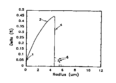
FIG. 1 is an illustrative chart showing a refractive index profile having a point
minimum.
FIG. 2 is an illustrative chart showing alternative refractive index profiles
havlng a polnt mlnlmum.
FIG. 3 is an illustrative chart showing an off axis trapezoidal ring index profile
and alternatives.
FIG. 4 is a step index embodiment of the novel refractive index profile.
Detailed Description of the Invention
Advantages of having two operating windows, i.e., two signal
wavelength ranges separated by a few hundred nanometers, are
- a system can be operated at only one window until rate demands justify
investing in a second window of operation;
- a second window can act as a redundant system for those
telecommunications links requiring essentially failure free operation; and,
- a second window can handle overflow from a primary window in systems
where there is a large data rate difference between peak demand and average
demand.
The present invention provides a dual window waveguide fiber having
the extra feature that non-linear effects, which can arise in high power densitysystems, wavelength division multiplex systems, or systems incorporating
optical amplifiers, are minimized. The novel waveguide fibers of this
application have high effective area in both the 1300 nm and 1550 nm
windows.
A first embodiment of the novel waveguide core profile is illustrated in
FIG. 1. The refractive index difference, 1, near the centerline is small, typically
less than about 0.20 %. The dopant level increases with radius, as indicated
by curve 2 until a maximum ~ % is reached. The final portion of the index
profile, 4, shows ~ % dropping off sharply to zero. There are several
equivalent index profiles wherein curve 4 can be altered without significantly
2192425
_
affecting the waveguide fiber properties. For example, 4 may be tilted outward
to increase the radius by about a micron or the junction of curves 4 and 2 may
be rounded. Also small additions to the refractive index profiie, such as those
indicated by curves 6, may be made without significant impact on waveguide
fiber properties. Thus it will be understood that FIG. 1 together with FIG. 2
represent a family of refractive index profiles which provide large effective area
at 1300 nm. Curves 8 of FIG. 2 show several members of the novel index
profile family. Again, curves 10 indicate the types of variations of the invented
index profile which still provide the required waveguide fiber properties.
An added benefit of the index profiles of FlG.'s 1 and 2, is that the
integrated dopant is lower as compared to a standard step index profile.
Hence the attenuation, which depends upon the dopant amount, will be lower
in the novel waveguide fiber.
Example 1 - Properties of a Point Minimum Waveguide
For the refractive index profiles shown by the solid curve in FIG. 1, the
following properties are calculated from the computer model:
- Ao is 1298 nm;
- Mode Field Diameter is 10.91 microns;
- Deff is 11.22 microns;
- Aeff is 98.9 microns2;
- Cut off wavelength is 1480 nm; and,
- Integrated GeO2 is 2.58.
Note that Deff is larger that mode field diameter and that Aeff is nearly
about 25 % higher than that of standard step index fiber.
For comparison, a step index fiber having the radius shown in FIG. 1,
and a ~ % of 0.36%, has properties:
- Ao is 1309 nm;
- Mode Field Diameter is 10.1 microns;
- Deff is 9.97 microns;
- Aeff is 78 microns2;
219~425
- Cut off wavelength is 1324 nm; and,
- Integrated GeO2 is 2.8. The effective area is much lower and the
dispersion zero, Ao1 is in the operating window, a characteristic unfavorable for
wavelength division multiplexed systems. The 9% increase in integrated GeO2
5 for the standard step index profile will result in higher waveguide attenuation
due to Rayleigh scattering. Both the larger effective area and the lower
attenuation of the novel waveguide fiber refractive index profile serve to
reduce adverse nonlinear effects.
The standard step index profile can be modified in a simple way to
10achieve large effective area. The profile may be characterized by ~ % of the
step, 18 in FIG. 4, and the radius 20. Table 1. shows the effect of l~ %
changes and radius changes on the effective area and the pin array bend
resistance.
Table 1
% Radius Aeff @1300 Aefl @1550 Pin Array
microns microns2 microns2 ~1550 dB
0.36 4.5 67 83 6.9
0.315 5.0 77 96 12.2
0.293 5.63 90 110 9.8
0.278 5.88 96 117 12.2
The trade off of bend resistance for larger effective area is clear.
Lowering the ~ % and increasing the radius clearly provides the required
larger effective areas. The step design having l~ % near 0.3% and radius near
25 5.6 microns has an acceptable bend resistance with significant improvement in
Aeff
A trapezoidal index profile spaced apart from the waveguide centerline
allows additional flexibility in the refractive index profile design to achieve
acceptable bend performance along with large effective areas at both
30 wavelength windows.
2192~25
The general shape of this embodiment of the novel waveguide fiber is
illustrated in FIG. 3. The trapezoidal shape 12 is spaced apart from the
waveguide centerline. The inside and outside radii of the trapezoidal core
index profile segment are 24 and 22 respectively. The refractive index profile
5 of the core segment adjacent the waveguide centerline may be substantially
flat or may have a shape as illustrated by curves 14. The required properties
of the novel waveguide may be obtained using slight variations of the
trapezoidal shape, as shown by curve 16 or by finding equivalent refractive
index profiles.
Table 2 provides modelled values for the trapezoidal embodiment of the
novel waveguide fiber. Under the column heading, 'Radii', the first number is
the inside radius of the trapezoid and the second number is the outside radius
thereof.
Table 2
% Radii microns Aeff @ 1330 Aeff @ 1550 Pin Array @
micron2 micronsZ 1550 dB
0.367 1.7 - 4.5 94 110 9.8
0.337 1.78 - 4.98 104 120 14.4
0.320 1.85 - 5.23 112 130 14.2
0.344 1.7 - 3.91 104 120 9.5
Excellent characteristics are shown by the profile designs of rows 1 and
4. These embodiments meet the requirements for an optical waveguide fiber
which limits nonlinear effects while retaining the needed bend resistance.
Tables 1 and 2 show that a computer model is essential for efficiently
identifying the refractive index profiles which meet a given set of performance
requirements. Comparing the distinct index profile designs, as given in the
rows of the tables, illustrates that small changes in index profile parameters
can have a large impact on waveguide properties. Thus, the number of
combinations and permutations which must be tried favor an approach wherein
computer modelling precedes manufacture of the waveguide fiber.
2192~25
Although particular embodiments of the invention have herein been
disclosed and described, the invention is nonetheless limited only by the
following claims.